
1
Data sheet acquired from Harris Semiconductor
SCHS211
Features
∑ Buffered Inputs
∑ Separate Serial Outputs Synchronous to Both
Positive and Negative Clock Edges For Cascading
∑ Fanout (Over Temperature Range)
- Standard Outputs . . . . . . . . . . . . . . . 10 LSTTL Loads
- Bus Driver Outputs . . . . . . . . . . . . . 15 LSTTL Loads
∑ Wide Operating Temperature Range . . . -55
o
C to 125
o
C
∑ Balanced Propagation Delay and Transition Times
∑ Significant Power Reduction Compared to LSTTL
Logic ICs
∑ HC Types
- 2V to 6V Operation
- High Noise Immunity: N
IL
= 30%, N
IH
= 30% of V
CC
at V
CC
= 5V
∑ HCT Types
- 4.5V to 5.5V Operation
- Direct LSTTL Input Logic Compatibility,
V
IL
= 0.8V (Max), V
IH
= 2V (Min)
- CMOS Input Compatibility, I
l
1
µ
A at V
OL
, V
OH
Pinout
CD74HC4094, CD74HCT4094
(PDIP, SOIC)
TOP VIEW
14
15
16
9
13
12
11
10
1
2
3
4
5
7
6
8
STROBE
DATA
CP
Q
0
Q
1
Q
2
GND
Q
3
V
CC
Q
4
Q
5
Q
6
Q
7
QS
2
QS
1
OE
November 1997
CAUTION: These devices are sensitive to electrostatic discharge. Users should follow proper IC Handling Procedures.
Copyright
©
Harris Corporation 1997
File Number
1779.1
CD74HC4094,
CD74HCT4094
High Speed CMOS Logic
8-Stage Shift and Store Bus Register, Three-State
[ /Title
(CD74H
C4094,
CD74H
CT4094
)
/Sub-
ject
(High
Speed
CMOS
Logic 8-
2
Description
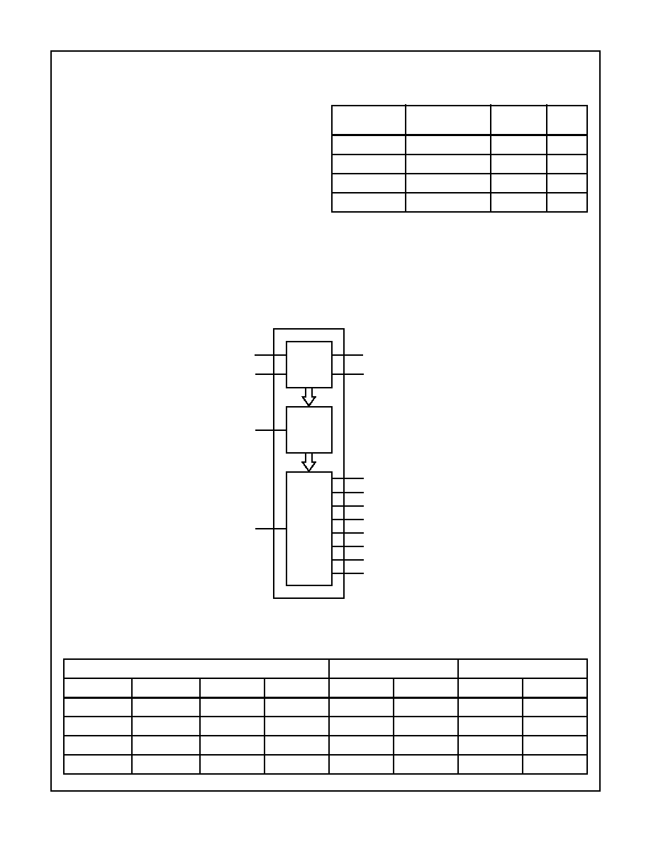
The Harris CD74HC4094 and CD74HCT4094 are 8-stage
serial shift registers having a storage latch associated with
each stage for strobing data from the serial input to parallel
buffered three-state outputs. The parallel outputs may be
connected directly to common bus lines. Data is shifted on
positive clock transitions. The data in each shift register
stage is transferred to the storage register when the Strobe
input is high. Data in the storage register appears at the
outputs whenever the Output-Enable signal is high.
Two serial outputs are available for cascading a number of
these devices. Data is available at the QS
1
serial output
terminal on positive clock edges to allow for high-speed
operation in cascaded system in which the clock rise time is
fast. The same serial information, available at the QS
2
terminal on the next negative clock edge, provides a means
for cascading these devices when the clock rise time is slow.
Functional Diagram
Ordering Information
PART NUMBER
TEMP. RANGE (
o
C)
PACKAGE
PKG.
NO.
CD74HC4094E
-55 to 125
16 Ld PDIP
E16.3
CD74HCT4094E
-55 to 125
16 Ld PDIP
E16.3
CD74HC4094M
-55 to 125
16 Ld SOIC
M16.15
CD74HCT4094M
-55 to 125
16 Ld SOIC
M16.15
NOTES:
1. When ordering, use the entire part number. Add the suffix 96 to
obtain the variant in the tape and reel.
2. Wafer or die for this part number is available which meets all elec-
trical specifications. Please contact your local sales office or
Harris customer service for ordering information.
GND = 8
V
CC
= 16
Q
2
6
7
Q
3
Q
1
5
Q
0
4
14
13
12
11
Q
4
Q
5
Q
6
Q
7
THREE-
OUTPUT
8-BIT
STORAGE
REGISTER
8-STAGE
SHIFT
REGISTER
OE
15
1
3
2
10
9
QS
2
QS
1
DATA
CP
STROBE
STATE
TRUTH TABLE
INPUTS
PARALLEL OUTPUTS
SERIAL OUTPUTS
CP
OE
STR
D
Q
0
Q
n
QS
1
(NOTE 4)
QS
2
L
X
X
Z
Z
Q'6
NC
L
X
X
Z
Z
NC
Q
7
H
L
X
NC
NC
Q'6
NC
H
H
L
L
Q
n
-1
Q'6
NC
CD74HC4094, CD74HCT4094

3
H
H
H
H
Q
n
-1
Q'6
NC
H
H
H
NC
NC
NC
Q
7
NOTES:
3. H = High Voltage Level, L = Low Voltage Level, X = Don't Care, NC = No charge, Z = High Impedance Off-state,
= Transition from Low to High Level,
= Transition from High to Low.
4. At the positive clock edge the information in the seventh register stage is transferred to the 8th register stage and QS
1
output.
TRUTH TABLE
INPUTS
PARALLEL OUTPUTS
SERIAL OUTPUTS
CP
OE
STR
D
Q
0
Q
n
QS
1
(NOTE 4)
QS
2
CD74HC4094, CD74HCT4094

4
Logic Diagram
FF
O
DQ
CP
CP
FF
1
FF
2
FF
3
FF
4
FF
5
FF
6
FF
7
L
8
CP
CP
Q
D
9
QS
1
QS
2
10
L
7
L
6
L
5
L
4
L
3
L
2
L
1
L
O
STR
STR
Q
DA
T
A
2
CP
3
STR
1
OE
15
Q
0
OE
OE
4
Q
1
5
Q
2
6
Q
3
7
Q
4
14
Q
5
13
Q
6
12
Q
7
11
CD74HC4094, CD74HCT4094
5
Absolute Maximum Ratings
Thermal Information
DC Supply Voltage, V
CC
. . . . . . . . . . . . . . . . . . . . . . . . -0.5V to 7V
DC Input Diode Current, I
IK
For V
I
< -0.5V or V
I
> V
CC
+ 0.5V
. . . . . . . . . . . . . . . . . . . . . .±
20mA
DC Output Diode Current, I
OK
For V
O
< -0.5V or V
O
> V
CC
+ 0.5V
. . . . . . . . . . . . . . . . . . . .±
20mA
DC Output Source or Sink Current per Output Pin, I
O
For V
O
> -0.5V or V
O
< V
CC
+ 0.5V
. . . . . . . . . . . . . . . . . . . .±
25mA
DC V
CC
or Ground Current, I
CC
. . . . . . . . . . . . . . . . . . . . . . . . .±
50mA
Operating Conditions
Temperature Range (T
A
) . . . . . . . . . . . . . . . . . . . . . -55
o
C to 125
o
C
Supply Voltage Range, V
CC
HC Types . . . . . . . . . . . . . . . . . . . . . . . . . . . . . . . . . . . . .2V to 6V
HCT Types . . . . . . . . . . . . . . . . . . . . . . . . . . . . . . . . .4.5V to 5.5V
DC Input or Output Voltage, V
I
, V
O
. . . . . . . . . . . . . . . . . 0V to V
CC
Input Rise and Fall Time
2V . . . . . . . . . . . . . . . . . . . . . . . . . . . . . . . . . . . . . . 1000ns (Max)
4.5V. . . . . . . . . . . . . . . . . . . . . . . . . . . . . . . . . . . . . . 500ns (Max)
6V . . . . . . . . . . . . . . . . . . . . . . . . . . . . . . . . . . . . . . . 400ns (Max)
Thermal Resistance (Typical, Note 5)
JA
(
o
C/W)
PDIP Package . . . . . . . . . . . . . . . . . . . . . . . . . . . . .
90
SOIC Package . . . . . . . . . . . . . . . . . . . . . . . . . . . . .
160
Maximum Junction Temperature . . . . . . . . . . . . . . . . . . . . . . . 150
o
C
Maximum Storage Temperature Range . . . . . . . . . .-65
o
C to 150
o
C
Maximum Lead Temperature (Soldering 10s) . . . . . . . . . . . . . 300
o
C
(SOIC - Lead Tips Only)
CAUTION: Stresses above those listed in "Absolute Maximum Ratings" may cause permanent damage to the device. This is a stress only rating and operation
of the device at these or any other conditions above those indicated in the operational sections of this specification is not implied.
NOTE:
5.
JA
is measured with the component mounted on an evaluation PC board in free air.
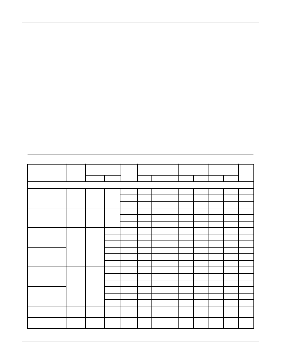
DC Electrical Specifications
PARAMETER
SYMBOL
TEST
CONDITIONS
V
CC
(V)
25
o
C
-40
o
C TO 85
o
C -55
o
C TO 125
o
C
UNITS
V
I
(V)
I
O
(mA)
MIN
TYP
MAX
MIN
MAX
MIN
MAX
HC TYPES
High Level Input
Voltage
V
IH
-
-
2
1.5
-
-
1.5
-
1.5
-
V
4.5
3.15
-
-
3.15
-
3.15
-
V
6
4.2
-
-
4.2
-
4.2
-
V
Low Level Input
Voltage
V
IL
-
-
2
-
-
0.5
-
0.5
-
0.5
V
4.5
-
-
1.35
-
1.35
-
1.35
V
6
-
-
1.8
-
1.8
-
1.8
V
High Level Output
Voltage
CMOS Loads
V
OH
V
IH
or V
IL
-0.02
2
1.9
-
-
1.9
-
1.9
-
V
-0.02
4.5
4.4
-
-
4.4
-
4.4
-
V
-0.02
6
5.9
-
-
5.9
-
5.9
-
V
High Level Output
Voltage
TTL Loads
-
-
-
-
-
-
-
-
-
V
-4
4.5
3.98
-
-
3.84
-
3.7
-
V
-5.2
6
5.48
-
-
5.34
-
5.2
-
V
Low Level Output
Voltage
CMOS Loads
V
OL
V
IH
or V
IL
0.02
2
-
-
0.1
-
0.1
-
0.1
V
0.02
4.5
-
-
0.1
-
0.1
-
0.1
V
0.02
6
-
-
0.1
-
0.1
-
0.1
V
Low Level Output
Voltage
TTL Loads
-
-
-
-
-
-
-
-
-
V
4
4.5
-
-
0.26
-
0.33
-
0.4
V
5.2
6
-
-
0.26
-
0.33
-
0.4
V
Input Leakage
Current
I
I
V
CC
or
GND
-
6
-
-
±
0.1
-
±
1
-
±
1
µ
A
Quiescent Device
Current
I
CC
V
CC
or
GND
0
6
-
-
8
-
80
-
160
µ
A
CD74HC4094, CD74HCT4094