1
Data sheet acquired from Harris Semiconductor
SCHS182
Features
∑ Common Latch Enable Control
∑ Common Three-State Output Enable Control
∑ Buffered Inputs
∑ Three-State Outputs
∑ Bus Line Driving Capacity
∑ Typical Propagation Delay = 12ns at V
CC
= 5V,
C
L
= 15pF, T
A
= 25
o
C (Data to Output for HC373)
∑ Fanout (Over Temperature Range)
- Standard Outputs . . . . . . . . . . . . . . . 10 LSTTL Loads
- Bus Driver Outputs . . . . . . . . . . . . . 15 LSTTL Loads
∑ Wide Operating Temperature Range . . . -55
o
C to 125
o
C
∑ Balanced Propagation Delay and Transition Times
∑ Significant Power Reduction Compared to LSTTL
Logic ICs
∑ HC Types
- 2V to 6V Operation
- High Noise Immunity: N
IL
= 30%, N
IH
= 30% of V
CC
at V
CC
= 5V
∑ HCT Types
- 4.5V to 5.5V Operation
- Direct LSTTL Input Logic Compatibility,
V
IL
= 0.8V (Max), V
IH
= 2V (Min)
- CMOS Input Compatibility, I
l
1
µ
A at V
OL
, V
OH
Description
The
Harris
CD74HC373,
CD74HCT373,
CD54HC573,
CD74HC573, and CD74HCT573 are high speed Octal Trans-
parent Latches manufactured with silicon gate CMOS technol-
ogy. They possess the low power consumption of standard
CMOS integrated circuits, as well as the ability to drive 15
LSTTL devices. The CD74HCT373 and CD74HCT573 are
functionally as well as pin compatible with the standard
74LS373 and 74LS573.
The outputs are transparent to the inputs when the latch
enable (LE) is high. When the latch enable (LE) goes low the
data is latched. The output enable (OE) controls the three-
state outputs. When the output enable (OE) is high the
outputs are in the high impedance state. The latch operation
is independent to the state of the output enable. The 373 and
573 are identical in function and differ only in their pinout
arrangements.
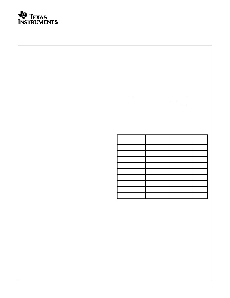
Ordering Information
PART NUMBER
TEMP. RANGE
(
o
C)
PACKAGE
PKG.
NO.
CD54HC573F
-55 to 125
20 Ld CERDIP
F20.3
CD74HC373E
-55 to 125
20 Ld PDIP
F20.3
CD74HCT373E
-55 to 125
20 Ld PDIP
E20.3
CD74HC573E
-55 to 125
20 Ld PDIP
E20.3
CD74HCT573E
-55 to 125
20 Ld PDIP
E20.3
CD74HC373M
-55 to 125
20 Ld SOIC
M20.3
CD74HCT373M
-55 to 125
20 Ld SOIC
M20.3
CD74HC573M
-55 to 125
20 Ld SOIC
M20.3
CD74HCT573M
-55 to 125
20 Ld SOIC
M20.3
NOTES:
1. When ordering, use the entire part number. Add the suffix 96 to
obtain the variant in the tape and reel.
2. Wafer or die for this part number are available which meets all
electrical specifications. Please contact your local sales office or
Harris customer service for ordering information.
November 1997
CAUTION: These devices are sensitive to electrostatic discharge. Users should follow proper IC Handling Procedures.
Copyright
©
Harris Corporation 1997
CD74HC373, CD74HCT373,
CD54HC573, CD74HC573,
CD74HCT573
High Speed CMOS Logic
Octal Transparent Latch, Three-State Output
File Number
1679.1
[ /Title
(CD74
HC373
,
CD74
HCT37
3,
CD54
HC573
,
CD74
HC573
,
CD74
HCT57
3)
/Sub-

2
Pinout
CD74HC373, CD74HCT373
(PDIP, SOIC)
TOP VIEW
CD54HC573, CD74HC573, CD74HCT573
(PDIP, SOIC, CERDIP)
TOP VIEW
Functional Block Diagrams
CD74HC373, CD74HCT373, CD74HC573, CD74HCT573
CD74HCT573
11
12
13
14
15
16
17
18
20
19
10
9
8
7
6
5
4
3
2
1
OE
Q0
D0
D1
Q1
Q2
D3
D2
Q3
GND
V
CC
D7
D6
Q6
Q7
Q5
D5
D4
Q4
LE
11
12
13
14
15
16
17
18
20
19
10
9
8
7
6
5
4
3
2
1
OE
D0
D1
D2
D3
D4
D6
D5
D7
GND
V
CC
Q1
Q2
Q3
Q0
Q4
Q5
Q6
Q7
LE
O
0
D
0
LE
OE
O
1
D
1
O
2
D
2
O
3
D
3
O
4
D
4
O
5
D
5
O
6
D
6
O
7
D
7
D
G
O
D
G
O
D
G
O
D
G
O
D
G
O
D
G
O
D
G
O
D
G
O
O
0
D
0
LE
OE
O
1
D
1
O
2
D
2
O
3
D
3
O
4
D
4
O
5
D
5
O
6
D
6
O
7
D
7
D
G
O
D
G
O
D
G
O
D
G
O
D
G
O
D
G
O
D
G
O
D
G
O
TRUTH TABLE
OUTPUT ENABLE
LATCH ENABLE
DATA
OUTPUT
L
H
H
H
L
H
L
L
L
L
l
L
L
L
h
H
H
X
X
Z
NOTE: H = High Voltage Level, L = Low Voltage Level, X = Don't Care, Z = High Impedance State, l = Low voltage level one set-up time prior
to the high to low latch enable transition, h = High voltage level one set-up time prior to the high to low latch enable transition.
CD74HC373, CD74HCT373, CD54HC573, CD74HC573, CD74HCT573

3
Absolute Maximum Ratings
Thermal Information
DC Supply Voltage, V
CC
. . . . . . . . . . . . . . . . . . . . . . . . -0.5V to 7V
DC Input Diode Current, I
IK
For V
I
< -0.5V or V
I
> V
CC
+ 0.5V
. . . . . . . . . . . . . . . . . . . . . .±
20mA
DC Output Diode Current, I
OK
For V
O
< -0.5V or V
O
> V
CC
+ 0.5V
. . . . . . . . . . . . . . . . . . . .±
20mA
DC Drain Current, per Output, I
O
For -0.5V < V
O
< V
CC
+ 0.5V
. . . . . . . . . . . . . . . . . . . . . . . . . .±
35mA
DC Output Source or Sink Current per Output Pin, I
O
For V
O
> -0.5V or V
O
< V
CC
+ 0.5V
. . . . . . . . . . . . . . . . . . . .±
25mA
DC V
CC
or Ground Current, I
CC
. . . . . . . . . . . . . . . . . . . . . . . . .±
50mA
Operating Conditions
Temperature Range, T
A
. . . . . . . . . . . . . . . . . . . . . . -55
o
C to 125
o
C
Supply Voltage Range, V
CC
HC Types . . . . . . . . . . . . . . . . . . . . . . . . . . . . . . . . . . . . .2V to 6V
HCT Types . . . . . . . . . . . . . . . . . . . . . . . . . . . . . . . . .4.5V to 5.5V
DC Input or Output Voltage, V
I
, V
O
. . . . . . . . . . . . . . . . . 0V to V
CC
Input Rise and Fall Time
2V . . . . . . . . . . . . . . . . . . . . . . . . . . . . . . . . . . . . . . 1000ns (Max)
4.5V. . . . . . . . . . . . . . . . . . . . . . . . . . . . . . . . . . . . . . 500ns (Max)
6V . . . . . . . . . . . . . . . . . . . . . . . . . . . . . . . . . . . . . . . 400ns (Max)
Thermal Resistance (Typical, Note 3)
. . . .
JA
(
o
C/W)
JA
(
o
C/W)
PDIP Package . . . . . . . . . . . . . . . . . . .
125
N/A
CERDIP Package . . . . . . . . . . . . . . . .
85
24
SOIC Package . . . . . . . . . . . . . . . . . . .
120
N/A
Maximum Junction Temperature (Plastic Package) . . . . . . . . 150
o
C
Maximum Storage Temperature Range . . . . . . . . . .-65
o
C to 150
o
C
Maximum Lead Temperature (Soldering 10s) . . . . . . . . . . . . . 300
o
C
(SOIC - Lead Tips Only)
CAUTION: Stresses above those listed in "Absolute Maximum Ratings" may cause permanent damage to the device. This is a stress only rating and operation
of the device at these or any other conditions above those indicated in the operational sections of this specification is not implied.
NOTE:
3.
JA
is measured with the component mounted on an evaluation PC board in free air.
DC Electrical Specifications
PARAMETER
SYMBOL
TEST
CONDITIONS
V
CC
(V)
25
o
C
-40
o
C TO 85
o
C
-55
o
C TO 125
o
C
UNITS
V
I
(V)
I
O
(mA)
MIN
TYP
MAX
MIN
MAX
MIN
MAX
HC TYPES
High Level Input
Voltage
V
IH
-
-
2
1.5
-
-
1.5
-
1.5
-
V
4.5
3.15
-
-
3.15
-
3.15
-
V
6
4.2
-
-
4.2
-
4.2
-
V
Low Level Input
Voltage
V
IL
-
-
2
-
-
0.5
-
0.5
-
0.5
V
4.5
-
-
1.35
-
1.35
-
1.35
V
6
-
-
1.8
-
1.8
-
1.8
V
High Level Output
Voltage
CMOS Loads
V
OH
V
IH
or
V
IL
-0.02
2
1.9
-
-
1.9
-
1.9
-
V
-0.02
4.5
4.4
-
-
4.4
-
4.4
-
V
-0.02
6
5.9
-
-
5.9
-
5.9
-
V
High Level Output
Voltage
TTL Loads
-6
4.5
3.98
-
-
3.84
-
3.7
-
V
-7.8
6
5.48
-
-
5.34
-
5.2
-
V
Low Level Output
Voltage
CMOS Loads
V
OL
V
IH
or
V
IL
0.02
2
-
-
0.1
-
0.1
-
0.1
V
0.02
4.5
-
-
0.1
-
0.1
-
0.1
V
0.02
6
-
-
0.1
-
0.1
-
0.1
V
Low Level Output
Voltage
TTL Loads
6
4.5
-
-
0.26
-
0.33
-
0.4
V
7.8
6
-
-
0.26
-
0.33
-
0.4
V
Input Leakage
Current
I
I
V
CC
or
GND
-
6
-
-
±
0.1
-
±
1
-
±
1
µ
A
Quiescent Device
Current
I
CC
V
CC
or
GND
0
6
-
-
8
-
80
-
160
µ
A
CD74HC373, CD74HCT373, CD54HC573, CD74HC573, CD74HCT573

4
Three-State Leakage
Current
-
V
IL
or
V
IH
V
O
=
V
CC
or
GND
6
-
-
±
0.5
-
±
5
-
±
10
µ
A
HCT TYPES
High Level Input
Voltage
V
IH
-
-
4.5 to
5.5
2
-
-
2
-
2
-
V
Low Level Input
Voltage
V
IL
-
-
4.5 to
5.5
-
-
0.8
-
0.8
-
0.8
V
High Level Output
Voltage
CMOS Loads
V
OH
V
IH
or
V
IL
-0.02
4.5
4.4
-
-
4.4
-
4.4
-
V
High Level Output
Voltage
TTL Loads
-6
4.5
3.98
-
-
3.84
-
3.7
-
V
-7.8
6
5.48
-
-
5.34
-
5.2
-
V
Low Level Output
Voltage
CMOS Loads
V
OL
V
IH
or
V
IL
0.02
4.5
-
-
0.1
-
0.1
-
0.1
V
Low Level Output
Voltage
TTL Loads
6
4.5
-
-
0.26
-
0.33
-
0.4
V
7.8
6
-
-
0.26
-
0.33
-
0.4
V
Input Leakage
Current
I
I
V
CC
to
GND
-
5.5
-
-
±
0.1
-
±
1
-
±
1
µ
A
Quiescent Device
Current
I
CC
V
CC
or
GND
0
5.5
-
-
8
-
80
-
160
µ
A
Three-State Leakage
Current
-
V
IL
or
V
IH
V
O
=
V
CC
or
GND
6
-
-
±
0.5
-
±
5
-
±
10
µ
A
Additional Quiescent
Device Current Per
Input Pin: 1 Unit Load
(Note 4)
I
CC
V
CC
-2.1
-
4.5 to
5.5
-
100
360
-
450
-
490
µ
A
NOTE:
4. For dual-supply systems theoretical worst case (V
I
= 2.4V, V
CC
= 5.5V) specification is 1.8mA.
DC Electrical Specifications
(Continued)
PARAMETER
SYMBOL
TEST
CONDITIONS
V
CC
(V)
25
o
C
-40
o
C TO 85
o
C
-55
o
C TO 125
o
C
UNITS
V
I
(V)
I
O
(mA)
MIN
TYP
MAX
MIN
MAX
MIN
MAX
HCT Input Loading Table
INPUT
UNIT LOADS
HCT373
HCT573
OE
1.5
1.25
Dn
0.4
0.3
LE
0.6
0.65
NOTE: Unit Load is
I
CC
limit specified in DC Electrical Specifica-
tions table, e.g., 360
µ
A max at 25
o
C.
CD74HC373, CD74HCT373, CD54HC573, CD74HC573, CD74HCT573

5
Prerequisite For Switching Specifications
PARAMETER
SYMBOL
TEST
CONDITIONS
V
CC
(V)
25
o
C
-40
o
C TO 85
o
C
-55
o
C TO 125
o
C
UNITS
MIN
TYP
MAX
MIN
MAX
MIN
MAX
HC TYPES
LE Pulse Width
t
W
-
2
80
-
-
100
-
120
-
ns
4.5
16
-
-
20
-
24
-
ns
6
14
-
-
17
-
20
-
ns
Set-up Time Data to LE
t
SU
-
2
50
-
-
65
-
75
-
ns
4.5
10
-
-
13
-
15
-
ns
6
9
-
-
11
-
13
-
ns
Hold Time, Data to LE
(573)
t
H
-
2
40
-
-
50
-
60
-
ns
4.5
8
-
-
10
-
12
-
ns
6
7
-
-
9
-
10
-
ns
Hold Time, Data to LE
(373)
t
H
-
2
5
-
-
5
-
5
-
ns
4.5
5
-
-
5
-
5
-
ns
6
5
-
-
5
-
5
-
ns
HCT TYPES
LE Pulse Width
t
w
-
4.5
16
-
-
20
-
24
-
ns
Set-up Time Data to LE
t
w
-
4.5
13
-
-
16
-
20
-
ns
Hold Time, Data to LE
t
H
-
4.5
10
-
-
13
-
15
-
ns
Switching Specifications
Input t
r
, t
f
= 6ns
PARAMETER
SYMBOL
TEST
CONDITIONS
V
CC
(V)
25
o
C
-40
o
C TO 85
o
C
-55
o
C TO
125
o
C
UNITS
TYP
MAX
MAX
MAX
HC TYPES
Propagation Delay,
Data to Qn
(HC/HCT373)
t
PLH
, t
PHL
C
L
= 50pF
2
-
150
190
225
ns
4.5
-
30
38
45
ns
6
-
26
33
38
ns
C
L
= 15pF
5
12
-
-
-
ns
Propagation Delay,
Data to Qn
(HC/HCT573)
t
PLH,
t
PHL
C
L
= 50pF
2
-
175
220
265
ns
4.5
-
35
44
53
ns
6
-
30
37
45
ns
C
L
= 15pF
5
14
-
-
-
ns
Propagation Delay,
LE to Qn
t
PLH,
t
PHL
C
L
= 50pF
2
-
175
220
265
ns
4.5
-
35
44
53
ns
6
-
30
37
45
ns
C
L
= 15pF
5
14
-
-
-
ns
CD74HC373, CD74HCT373, CD54HC573, CD74HC573, CD74HCT573