
1
Data sheet acquired from Harris Semiconductor
SCHS124D
Features
∑ Hysteresis on Clock Inputs for Improved Noise
Immunity and Increased Input Rise and Fall Times
∑ Asynchronous Set and Reset
∑ Complementary Outputs
∑ Buffered Inputs
∑ Typical f
MAX
= 50MHz at V
CC
= 5V, C
L
= 15pF,
T
A
= 25
o
C
∑ Fanout (Over Temperature Range)
- Standard Outputs . . . . . . . . . . . . . . . 10 LSTTL Loads
- Bus Driver Outputs . . . . . . . . . . . . . 15 LSTTL Loads
∑ Wide Operating Temperature Range . . . -55
o
C to 125
o
C
∑ Balanced Propagation Delay and Transition Times
∑ Significant Power Reduction Compared to LSTTL
Logic ICs
∑ HC Types
- 2V to 6V Operation
- High Noise Immunity: N
IL
= 30%, N
IH
= 30% of V
CC
at V
CC
= 5V
∑ HCT Types
- 4.5V to 5.5V Operation
- Direct LSTTL Input Logic Compatibility,
V
IL
= 0.8V (Max), V
IH
= 2V (Min)
- CMOS Input Compatibility, I
l
1
µ
A at V
OL
, V
OH
Description
The 'HC74 and 'HCT74 utilize silicon gate CMOS technology
to achieve operating speeds equivalent to LSTTL parts.
They exhibit the low power consumption of standard CMOS
integrated circuits, together with the ability to drive 10 LSTTL
loads.
This flip-flop has independent DATA, SET, RESET and
CLOCK inputs and Q and Q outputs. The logic level present
at the data input is transferred to the output during the
positive-going transition of the clock pulse. SET and RESET
are independent of the clock and are accomplished by a low
level at the appropriate input.
The HCT logic family is functionally as well as pin compatible
with the standard LS logic family.
Ordering Information
PART NUMBER
TEMP. RANGE
(
o
C)
PACKAGE
CD54HC74F3A
-55 to 125
14 Ld CERDIP
CD54HCT74F3A
-55 to 125
14 Ld CERDIP
CD74HC74E
-55 to 125
14 Ld PDIP
CD74HC74M
-55 to 125
14 Ld SOIC
CD74HC74MT
-55 to 125
14 Ld SOIC
CD74HC74M96
-55 to 125
14 Ld SOIC
CD74HCT74E
-55 to 125
14 Ld PDIP
CD74HCT74M
-55 to 125
14 Ld SOIC
CD74HCT74MT
-55 to 125
14 Ld SOIC
CD74HCT74M96
-55 to 125
14 Ld SOIC
NOTE: When ordering, use the entire part number. The suffix 96
denotes tape and reel. The suffix T denotes a small-quantity reel of
250.
CAUTION: These devices are sensitive to electrostatic discharge. Users should follow proper IC Handling Procedures.
Copyright
©
2003, Texas Instruments Incorporated
CD54HC74, CD74HC74,
CD54HCT74, CD74HCT74
Dual D Flip-Flop with Set and Reset
Positive-Edge Trigger
[ /Title
(CD54H
C74,
CD74H
C74,
CD74H
CT74)
/Subject
(Dual D
Flip-
Flop
with Set
January 1998 - Revised September 2003

2
Pinout
CD54HC74, CD54HCT74
(CERDIP)
CD74HC74, CD74HCT74
(PDIP, SOIC)
TOP VIEW
Functional Diagram
TRUTH TABLE
INPUTS
OUTPUTS
SET
RESET
CP
D
Q
Q
L
H
X
X
H
L
H
L
X
X
L
H
L
L
X
X
H (Note 1)
H (Note 1)
H
H
H
H
L
H
H
L
L
H
H
H
L
X
Q0
Q0
H= High Level (Steady State)
L= Low Level (Steady State)
X= Don't Care
= Low-to-High Transition
Q0 = the level of Q before the indicated input conditions were established.
NOTE:
1. This configuration is nonstable, that is, it will not persist when set and reset inputs return to their inactive (high) level.
1R
1D
1CP
1S
1Q
1Q
GND
V
CC
2R
2D
2CP
2S
2Q
2Q
1
2
3
4
5
6
7
14
13
12
11
10
9
8
RESET
DATA
RESET
SET
1
2
3
13
5
6
Q
Q
10
CLOCK
4
SET
DATA
12
11
9
8
Q
Q
CLOCK
D
CP
R
F/F 2
S
GND = PIN 7
V
CC
= PIN 14
D
CP
R
F/F 1
S
CD54HC74, CD74HC74, CD54HCT74, CD74HCT74
3
Absolute Maximum Ratings
Thermal Information
DC Supply Voltage, V
CC
. . . . . . . . . . . . . . . . . . . . . . . . -0.5V to 7V
DC Input Diode Current, I
IK
For V
I
< -0.5V or V
I
> V
CC
+ 0.5V
. . . . . . . . . . . . . . . . . . . . . .±
20mA
DC Drain Current, per Output, I
O
For -0.5V < V
O
< V
CC
+ 0.5V
. . . . . . . . . . . . . . . . . . . . . . . . . .±
25mA
DC Output Diode Current, I
OK
For V
O
< -0.5V or V
O
> V
CC
+ 0.5V
. . . . . . . . . . . . . . . . . . . .±
20mA
DC Output Source or Sink Current per Output Pin, I
O
For V
O
> -0.5V or V
O
< V
CC
+ 0.5V
. . . . . . . . . . . . . . . . . . . .±
25mA
DC V
CC
or Ground Current, I
CC
. . . . . . . . . . . . . . . . . . . . . . . . .±
50mA
Operating Conditions
Temperature Range (T
A
) . . . . . . . . . . . . . . . . . . . . . -55
o
C to 125
o
C
Supply Voltage Range, V
CC
HC Types . . . . . . . . . . . . . . . . . . . . . . . . . . . . . . . . . . . . .2V to 6V
HCT Types . . . . . . . . . . . . . . . . . . . . . . . . . . . . . . . . .4.5V to 5.5V
DC Input or Output Voltage, V
I
, V
O
. . . . . . . . . . . . . . . . . 0V to V
CC
Input Rise and Fall Time
2V . . . . . . . . . . . . . . . . . . . . . . . . . . . . . . . . . . . . . . 1000ns (Max)
4.5V. . . . . . . . . . . . . . . . . . . . . . . . . . . . . . . . . . . . . . 500ns (Max)
6V . . . . . . . . . . . . . . . . . . . . . . . . . . . . . . . . . . . . . . . 400ns (Max)
Thermal Resistance (Typical, Note 2)
JA
(
o
C/W)
E (PDIP) Package . . . . . . . . . . . . . . . . . . . . . . . . . . . . . . 80
M (SOIC) Package. . . . . . . . . . . . . . . . . . . . . . . . . . . . . . 86
Maximum Junction Temperature (Hermetic Package or Die) . . . 175
o
C
Maximum Junction Temperature (Plastic Package) . . . . . . . . 150
o
C
Maximum Storage Temperature Range . . . . . . . . . .-65
o
C to 150
o
C
Maximum Lead Temperature (Soldering 10s) . . . . . . . . . . . . . 300
o
C
(SOIC - Lead Tips Only)
CAUTION: Stresses above those listed in "Absolute Maximum Ratings" may cause permanent damage to the device. This is a stress only rating and operation
of the device at these or any other conditions above those indicated in the operational sections of this specification is not implied.
NOTE:
2. The package thermal impedance is calculated in accordance with JESD 51-7.
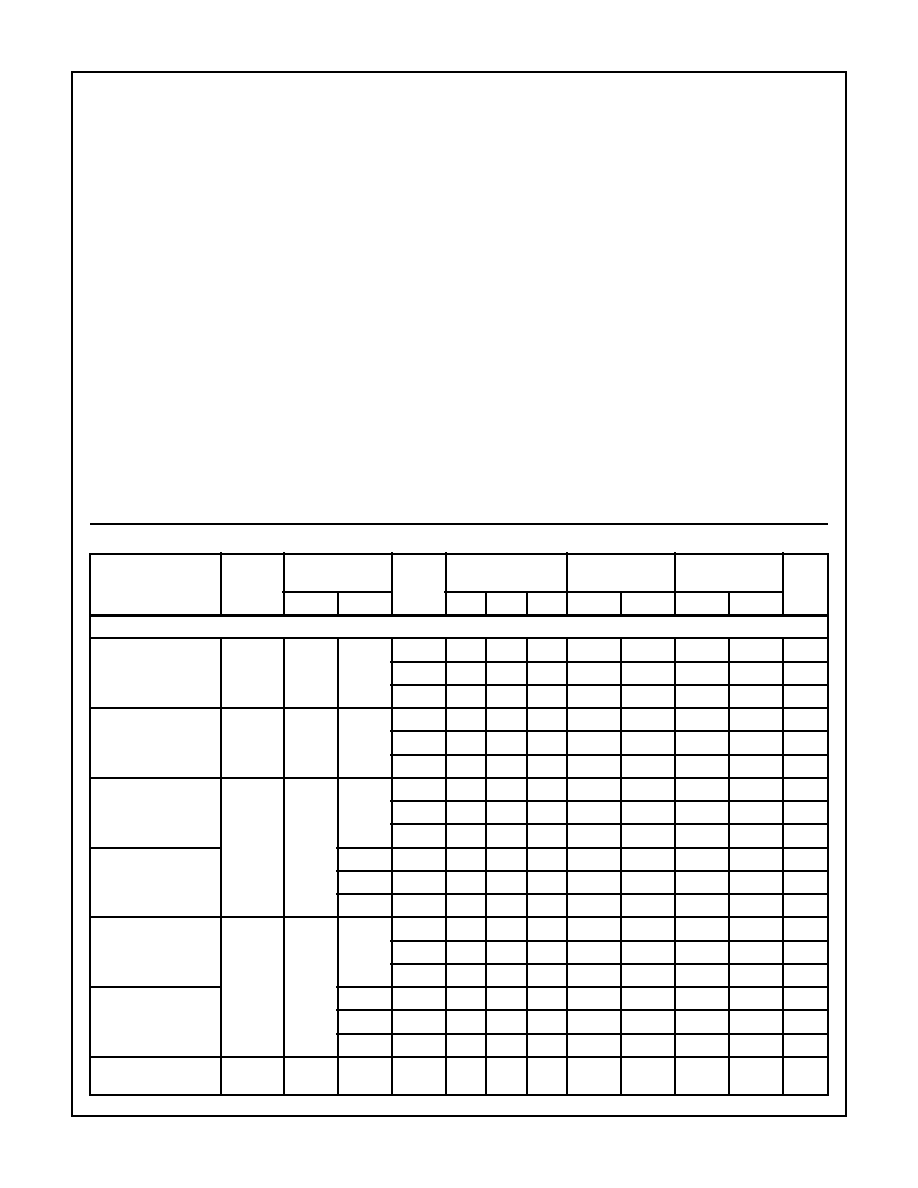
DC Electrical Specifications
PARAMETER
SYMBOL
TEST
CONDITIONS
V
CC
(V)
25
o
C
-40
o
C TO 85
o
C
-55
o
C TO 125
o
C
UNITS
V
I
(V)
I
O
(mA)
MIN
TYP
MAX
MIN
MAX
MIN
MAX
HC TYPES
High Level Input
Voltage
V
IH
-
-
2
1.5
-
-
1.5
-
1.5
-
V
4.5
3.15
-
-
3.15
-
3.15
-
V
6
4.2
-
-
4.2
-
4.2
-
V
Low Level Input
Voltage
V
IL
-
-
2
-
-
0.5
-
0.5
-
0.5
V
4.5
-
-
1.35
-
1.35
-
1.35
V
6
-
-
1.8
-
1.8
-
1.8
V
High Level Output
Voltage
CMOS Loads
V
OH
V
IH
or
V
IL
-0.02
2
1.9
-
-
1.9
-
1.9
-
V
4.5
4.4
-
-
4.4
-
4.4
-
V
6
5.9
-
-
5.9
-
5.9
-
V
High Level Output
Voltage
TTL Loads
-
-
-
-
-
-
-
-
-
V
-4
4.5
3.98
-
-
3.84
-
3.7
-
V
-5.2
6
5.48
-
-
5.34
-
5.2
-
V
Low Level Output
Voltage
CMOS Loads
V
OL
V
IH
or
V
IL
0.02
2
-
-
0.1
-
0.1
-
0.1
V
4.5
-
-
0.1
-
0.1
-
0.1
V
6
-
-
0.1
-
0.1
-
0.1
V
Low Level Output
Voltage
TTL Loads
-
-
-
-
-
-
-
-
-
V
4
4.5
-
-
0.26
-
0.33
-
0.4
V
5.2
6
-
-
0.26
-
0.33
-
0.4
V
Input Leakage
Current
I
I
V
CC
or
GND
-
6
-
-
±
0.1
-
±
1
-
±
1
µ
A
CD54HC74, CD74HC74, CD54HCT74, CD74HCT74

4
Quiescent Device
Current
I
CC
V
CC
or
GND
0
6
-
-
4
-
40
-
80
µ
A
HCT TYPES
High Level Input
Voltage
V
IH
-
-
4.5 to
5.5
2
-
-
2
-
2
-
V
Low Level Input
Voltage
V
IL
-
-
4.5 to
5.5
-
-
0.8
-
0.8
-
0.8
V
High Level Output
Voltage
CMOS Loads
V
OH
V
IH
or
V
IL
-0.02
4.5
4.4
-
-
4.4
-
4.4
-
V
High Level Output
Voltage
TTL Loads
-4
4.5
3.98
-
-
3.84
-
3.7
-
V
Low Level Output
Voltage CMOS Loads
V
OL
V
IH
or
V
IL
0.02
4.5
-
-
0.1
-
0.1
-
0.1
V
Low Level Output
Voltage
TTL Loads
4
4.5
-
-
0.26
-
0.33
-
0.4
V
Input Leakage
Current
I
I
V
CC
and
GND
-
5.5
-
±
0.1
-
±
1
-
±
1
µ
A
Quiescent Device
Current
I
CC
V
CC
or
GND
0
5.5
-
-
4
-
40
-
80
µ
A
Additional Quiescent
Device Current Per
Input Pin: 1 Unit Load
I
CC
(Note 3)
V
CC
- 2.1
-
4.5 to
5.5
-
100
360
-
450
-
490
µ
A
NOTE:
3. For dual-supply systems theoretical worst case (V
I
= 2.4V, V
CC
= 5.5V) specification is 1.8mA.
DC Electrical Specifications
(Continued)
PARAMETER
SYMBOL
TEST
CONDITIONS
V
CC
(V)
25
o
C
-40
o
C TO 85
o
C
-55
o
C TO 125
o
C
UNITS
V
I
(V)
I
O
(mA)
MIN
TYP
MAX
MIN
MAX
MIN
MAX
HCT Input Loading Table
INPUT
UNIT LOADS
D
0.5
R
0.5
CP
0.7
S
0.75
NOTE: Unit Load is
I
CC
limit specified in DC Electrical Specifica-
tions table, e.g., 360
µ
A max at 25
o
C.
Prerequisite For Switching Specifications
PARAMETER
SYMBOL
TEST
CONDITIONS
V
CC
(V)
25
o
C
-40
o
C TO 85
o
C
-55
o
C TO 125
o
C
UNITS
MIN
TYP
MAX
MIN
MAX
MIN
MAX
HC TYPES
Data to CP Setup Time
(Figure 5)
t
SU
-
2
60
-
-
75
-
90
-
ns
4.5
12
-
-
15
-
18
-
ns
6
10
-
-
13
-
15
-
ns
CD54HC74, CD74HC74, CD54HCT74, CD74HCT74

5
Hold Time (Figure 5)
t
H
-
2
3
-
-
3
-
3
-
ns
4.5
3
-
-
3
-
3
-
ns
6
3
-
-
3
-
3
-
ns
Removal Time R, S, to CP
(Figure 5)
t
REM
-
2
30
-
-
40
-
45
-
ns
4.5
6
-
-
8
-
9
-
ns
6
5
-
-
7
-
8
-
ns
Pulse Width R, S (Figure 1)
t
W
-
2
80
-
-
100
-
120
-
ns
4.5
16
-
-
20
-
24
-
ns
6
14
-
-
17
-
20
-
ns
Pulse Width CP (Figure 1)
t
W
-
2
80
-
-
100
-
120
-
ns
4.5
16
-
-
20
-
24
-
ns
6
14
-
-
17
-
20
-
ns
CP Frequency
f
MAX
-
2
6
-
-
5
-
4
-
MHz
4.5
30
-
-
25
-
20
-
MHz
6
35
-
-
29
-
23
-
MHz
HCT TYPES
Data to CP Setup Time
(Figure 6)
t
SU
-
4.5
12
-
-
15
-
18
-
ns
Hold Time (Figure 6)
t
H
-
4.5
3
-
-
3
-
3
-
ns
Removal Time R, S, to CP
(Figure 6)
t
REM
-
4.5
6
-
-
8
-
9
-
ns
Pulse Width R, S (Figure 2)
t
W
-
4.5
16
-
-
20
-
24
-
ns
Pulse Width CP (Figure 2)
t
W
-
4.5
18
-
-
23
-
27
-
ns
CP Frequency
f
MAX
-
4.5
25
-
-
20
-
16
-
MHz
Switching Specifications
Input t
r
, t
f
= 6ns
PARAMETER
SYMBOL
TEST
CONDITIONS
V
CC
(V)
25
o
C
-40
o
C TO 85
o
C
-55
o
C TO 125
o
C
UNITS
MIN
TYP
MAX
MIN
MAX
MIN
MAX
HC TYPES
Propagation Delay,
CP to Q, Q (Figure 3)
t
PLH
, t
PHL
C
L
= 50pF
2
-
-
175
-
220
-
265
ns
C
L
= 50pF
4.5
-
-
35
-
44
-
53
ns
C
L
= 15pF
5
-
14
-
-
-
-
-
ns
C
L
= 50pF
6
-
-
30
-
37
-
45
ns
Propagation Delay,
R, S to Q, Q (Figure 3)
t
PLH
, t
PHL
C
L
= 50pF
2
-
-
200
-
250
-
300
ns
C
L
= 50pF
4.5
-
-
40
-
50
-
60
ns
C
L
= 15pF
5
-
17
-
-
-
-
-
ns
C
L
= 50pF
6
-
-
34
-
43
-
51
ns
Transition Time (Figure 3)
t
TLH
, t
THL
C
L
= 50pF
2
-
-
75
-
95
-
110
ns
C
L
= 50pF
4.5
-
-
15
-
19
-
22
ns
C
L
= 50pF
6
-
-
13
-
16
-
19
ns
Input Capacitance
C
I
-
-
-
-
10
-
10
-
10
pF
Prerequisite For Switching Specifications
(Continued)
PARAMETER
SYMBOL
TEST
CONDITIONS
V
CC
(V)
25
o
C
-40
o
C TO 85
o
C
-55
o
C TO 125
o
C
UNITS
MIN
TYP
MAX
MIN
MAX
MIN
MAX
CD54HC74, CD74HC74, CD54HCT74, CD74HCT74