
CDCVF2505
3.3-V CLOCK PHASE-LOCK LOOP CLOCK DRIVER
SCAS640D ≠ JULY 2000 ≠ REVISED JULY 2002
1
POST OFFICE BOX 655303
∑
DALLAS, TEXAS 75265
D
Phase-Lock Loop Clock Driver for
Synchronous DRAM and General-Purpose
Applications
D
Spread Spectrum Clock Compatible
D
Operating Frequency: 24 MHz to 200 MHz
D
Low Jitter (Cycle-cycle): <|150 ps| Over the
Range 66 MHz≠200 MHz
D
Distributes One Clock Input to One Bank of
Five Outputs (CLKOUT Is Used to Tune the
Input-Output Delay)
D
Three-States Outputs When There Is no
Input Clock
D
Operates From Single 3.3-V Supply
D
Available in 8-Pin TSSOP and 8-Pin SOIC
Packages
D
Consumes Less Than 100
µ
A (Typically) in
Power Down Mode
D
Internal Feedback Loop Is Used to
Synchronize the Outputs to the Input Clock
D
25-
On-Chip Series Damping Resistors
D
Integrated RC PLL Loop Filter Eliminates
the Need for External Components
description
The CDCVF2505 is a high-performance, low-skew, low-jitter, phase-lock loop (PLL) clock driver. It uses a PLL
to precisely align, in both frequency and phase, the output clocks (1Y[0≠3] and CLKOUT) to the input clock
signal (CLKIN). The CDCVF2505 operates at 3.3 V. It also provides integrated series-damping resistors that
make it ideal for driving point-to-point loads.
One bank of five outputs provides low-skew, low-jitter copies of CLKIN. Output duty cycles are adjusted to 50
percent, independent of duty cycle at CLKIN. The device automatically goes in power-down mode when no input
signal is applied to CLKIN.
Unlike many products containing PLLs, the CDCVF2505 does not require an external RC network. The loop
filter for the PLLs is included on-chip, minimizing component count, space, and cost.
Because it is based on the PLL circuitry, the CDCVF2505 requires a stabilization time to achieve phase lock
of the feedback signal to the reference signal. This stabilization is required following power up and application
of a fixed-frequency, fixed-phase signal at CLKIN, and following any changes to the PLL reference.
The CDCVF2505 is characterized for operation from ≠40
∞
C to 85
∞
C.
Copyright
2002, Texas Instruments Incorporated
PRODUCTION DATA information is current as of publication date.
Products conform to specifications per the terms of Texas Instruments
standard warranty. Production processing does not necessarily include
testing of all parameters.
Please be aware that an important notice concerning availability, standard warranty, and use in critical applications of
Texas Instruments semiconductor products and disclaimers thereto appears at the end of this data sheet.
1
2
3
4
8
7
6
5
CLKIN
1Y1
1Y0
GND
CLKOUT
1Y3
V
DD
3.3 V
1Y2
D OR PW PACKAGE
(TOP VIEW)
CDCVF2505
3.3-V CLOCK PHASE-LOCK LOOP CLOCK DRIVER
SCAS640D ≠ JULY 2000 ≠ REVISED JULY 2002
2
POST OFFICE BOX 655303
∑
DALLAS, TEXAS 75265
FUNCTION TABLE
INPUT
OUTPUTS
CLKIN
1Y (0:3)
CLKOUT
L
H
<10 MHz
L
H
Z
L
H
Z
Typically, below 2 MHz the device goes in power-down mode in
which the PLL is turned off and the outputs enter into Hi-Z mode. If
a >10-MHz signal is applied at CLKIN the PLL turns on, reacquires
lock, and stabilizes after approximately 100
µ
s. The outputs will then
be enabled.
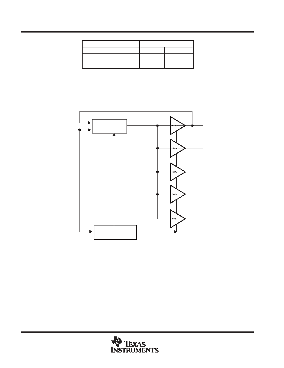
functional block diagram
Edge Detect
Typical <10 MHz
Power Down
3-State
1
8
3
2
5
7
CLKOUT
1Y0
1Y1
1Y2
1Y3
CLKIN
PLL
25
25
25
25
25

CDCVF2505
3.3-V CLOCK PHASE-LOCK LOOP CLOCK DRIVER
SCAS640D ≠ JULY 2000 ≠ REVISED JULY 2002
3
POST OFFICE BOX 655303
∑
DALLAS, TEXAS 75265
Terminal Functions
TERMINAL
I/O
DESCRIPTION
NAME
NO.
I/O
DESCRIPTION
1Y[0≠3]
2, 3, 5, 7
O
Clock outputs. These outputs are low-skew copies of CLKIN. Each output has an integrated 25-
series damping resistor.
CLKIN
1
I
Clock input. CLKIN provides the clock signal to be distributed by the CDCVF2505 clock driver.
CLKIN is used to provide the reference signal to the integrated PLL that generates the clock output
signals. CLKIN must have a fixed frequency and fixed phase for the PLL to obtain phase lock. Once
the circuit is powered up and a valid signal is applied, a stabilization time (100
µ
s) is required for the
PLL to phase lock the feedback signal to CLKIN.
CLKOUT
8
O
Feedback output. CLKOUT completes the internal feedback loop of the PLL. This connection is
made inside the chip and an external feedback loop should NOT be connected. CLKOUT can be
loaded with a capacitor to achieve zero delay between CLKIN and the Y outputs.
GND
4
Power
Ground
VDD3.3V
6
Power
3.3-V Supply
absolute maximum ratings over operating free-air temperature (unless otherwise noted)
Supply voltage range, V
DD
≠0.5 V to 4.3 V
. . . . . . . . . . . . . . . . . . . . . . . . . . . . . . . . . . . . . . . . . . . . . . . . . . . . . . . . .
Input voltage range, V
I
(see Notes 1 and 2)
≠0.5 V to V
DD
+ 0.5 V
. . . . . . . . . . . . . . . . . . . . . . . . . . . . . . . . . . . .
Output voltage range, V
O
(see Notes 1 and 2)
≠0.5 V to V
DD
+ 0.5 V
. . . . . . . . . . . . . . . . . . . . . . . . . . . . . . . . . .
Input clamp current, I
IK
(V
I
< 0 or V
I
> V
DD
)
±
50 mA
. . . . . . . . . . . . . . . . . . . . . . . . . . . . . . . . . . . . . . . . . . . . . . . .
Output clamp current, I
OK
(V
O
< 0 or V
O
> V
DD
)
±
50 mA
. . . . . . . . . . . . . . . . . . . . . . . . . . . . . . . . . . . . . . . . . . . .
Continuous total output current, I
O
(V
O
= 0 to V
DD
)
±
50 mA
. . . . . . . . . . . . . . . . . . . . . . . . . . . . . . . . . . . . . . . . .
Package thermal impedance,
JA
(see Note 3): D package
165.5
∞
C/W
. . . . . . . . . . . . . . . . . . . . . . . . . . . . . . .
PWR package
230.5
∞
C/W
. . . . . . . . . . . . . . . . . . . . . . . . . . . .
Storage temperature range, T
stg
≠ 65
∞
C to 150
∞
C
. . . . . . . . . . . . . . . . . . . . . . . . . . . . . . . . . . . . . . . . . . . . . . . . . . .
Stresses beyond those listed under "absolute maximum ratings" may cause permanent damage to the device. These are stress ratings only, and
functional operation of the device at these or any other conditions beyond those indicated under "recommended operating conditions" is not
implied. Exposure to absolute-maximum-rated conditions for extended periods may affect device reliability.
NOTES:
1. The input and output negative-voltage ratings may be exceeded if the input and output clamp-current ratings are observed.
2. This value is limited to 4.3 V maximum.
3. The package thermal impedance is calculated in accordance with JESD 51.
recommended operating conditions
MIN
NOM
MAX
UNIT
Supply voltage, VDD
3
3.3
3.6
V
High-level input voltage, VIH
0.7 VDD
V
Low-level input voltage, VIL
0.3 VDD
V
Input voltage, VI
0
VDD
V
High-level output current, IOH
≠12
mA
Low-level output current, IOL
12
mA
Operating free-air temperature, TA
≠40
85
∞
C

CDCVF2505
3.3-V CLOCK PHASE-LOCK LOOP CLOCK DRIVER
SCAS640D ≠ JULY 2000 ≠ REVISED JULY 2002
4
POST OFFICE BOX 655303
∑
DALLAS, TEXAS 75265
timing requirements over recommended ranges of supply voltage and operating free-air
temperature
MIN
NOM
MAX
UNIT
fclk
Clock frequency
24
200
MHz
Input clock duty cycle
24 MHz ≠ 85 MHz (see Note 4)
30%
85%
Input clock duty cycle
86 MHz ≠ 200 MHz
40%
50%
60%
Stabilization time (see Note 5)
100
µ
s
NOTES:
4. Ensured by design but not 100% production tested.
5. Time required for the integrated PLL circuit to obtain phase lock of its feedback signal to its reference signal. For phase lock to be
obtained, a fixed-frequency, fixed-phase reference signal must be present at CLKIN. Until phase lock is obtained, the specifications
for propagation delay, skew, and jitter parameters given in the switching characteristics table are not applicable. This parameter does
not apply for input modulation under SSC application.
electrical characteristics over recommended operating free-air temperature range (unless
otherwise noted)
PARAMETER
TEST CONDITIONS
VDD
MIN
TYP
MAX
UNIT
VIK
Input voltage
II = ≠18 mA
3 V
≠1.2
V
V
High-level output voltage
IOH = ≠100
µ
A
MIN to MAX
VDD≠0.2
V
VOH
High-level output voltage
IOH = ≠12 mA
3 V
2.1
V
OH
IOH = ≠6 mA
3 V
2.4
V
Low-level output voltage
IOL = 100
µ
A
MIN to MAX
0.2
V
VOL
Low-level output voltage
IOL = 12 mA
3 V
0.8
V
OL
IOL = 6 mA
3 V
0.55
IOH
High-level output current
VO = 1 V
3 V
≠27
mA
IOH
High-level output current
VO = 1.65 V
3.3 V
≠36
mA
IOL
Low-level output current
VO = 2 V
3 V
27
mA
IOL
Low-level output current
VO = 1.65 V
3.3 V
40
mA
II
Input current
VI = 0 V or VDD
±
5
µ
A
Ci
Input capacitance
VI = 0 V or VDD
3.3 V
4.2
pF
Co
Output capacitance
Yn
VI = 0 V or VDD
3.3 V
2.8
pF
Co
Output capacitance
CLKOUT
VI = 0 V or VDD
3.3 V
5.2
pF
All typical values are at respective nominal VDD and 25
∞
C.
switching characteristics over recommended ranges of supply voltage and operating free-air
temperature, C
L
= 25 pF, V
DD
= 3.3 V
±
0.3 V (see Note 5)
PARAMETER
TEST CONDITIONS
MIN
TYP
MAX
UNIT
tpd
Propagation delay (normalized (see Figure 3)
CLKIN to Yn, f= 66 MHz to 200 MHz
≠150
150
ps
tsk(o)
Output skew (see Note 6)
Yn to Yn
150
ps
tc(jit_cc)
Jitter (cycle to cycle) (see Figure 5)
f = 66 MHz to 200 MHz
70
150
ps
tc(jit_cc)
Jitter (cycle to cycle) (see Figure 5)
f = 24 MHz to 50 MHz
200
400
ps
odc
Output duty cycle (see Figure 4)
f = 24 MHz to 200 MHz at 50% VDD
45%
55%
tr
Rise time
VO = 0.4 V to 2 V
0.5
2
ns
tf
Fall time
VO = 2 V to 0.4 V
0.5
2
ns
All typical values are at respective nominal VDD and 25
∞
C.
NOTE 6: The tsk(o) specification is only valid for equal loading of all outputs.

CDCVF2505
3.3-V CLOCK PHASE-LOCK LOOP CLOCK DRIVER
SCAS640D ≠ JULY 2000 ≠ REVISED JULY 2002
5
POST OFFICE BOX 655303
∑
DALLAS, TEXAS 75265
ESD information
ESD MODELS
LIMIT
Human Body Model (HBM)
2.0 kV
Machine Model (MM)
300 V
Charge Device Model (CDM)
1 kV
thermal information
CDCVF2505 8-PIN SOIC
THERMAL AIR FLOW (CFM)
UNIT
CDCVF2505 8-PIN SOIC
0
150
250
500
UNIT
R
JA
High K
97
87
83
77
∞
C/W
R
JA
Low K
165
126
113
97
∞
C/W
R
JC
High K
39
∞
C/W
R
JC
Low K
42
∞
C/W
CDCVF2505 8-PIN TSSOP
THERMAL AIR FLOW (CFM)
UNIT
CDCVF2505 8-PIN TSSOP
0
150
250
500
UNIT
R
JA
High K
149
142
138
132
∞
C/W
R
JA
Low K
230
185
170
150
∞
C/W
R
JC
High K
65
∞
C/W
R
JC
Low K
69
∞
C/W
TYPICAL CHARACTERISTICS
Figure 1
≠1400
≠1050
≠700
≠350
0
350
700
1050
1400
≠30
≠20
≠10
0
10
20
30
≠ Propagation Delay T
ime ≠ ps
t
pd
,
PROPAGATION DELAY TIME
vs
DELTA LOAD (TYPICAL VALUES @ 3.3 V, 25
∞
C)
t pd
Delta Load ≠ pF
Yn = 25 pF || 500
NOTE: Delta Load = CLKOUT Load ≠ Yn Load
Figure 2
0
100
200
300
400
500
25
50
75
100
125
150
175
200
f ≠ Frequency ≠ MHz
≠ Propagation Delay T
ime ≠ ps
t
pd,
PROPAGATION DELAY TIME
vs
FREQUENCY (TYPICAL VALUES @ 3.3 V, 25
∞
C)
t pd
Load: CLKOUT = 12 pF || 500
,
Yn = 25 pF || 500