Äîêóìåíòàöèÿ è îïèñàíèÿ www.docs.chipfind.ru
8-Bit Register
CY54/74FCT273T
SCCS020 - March 1995 - Revised February 2000
Data sheet acquired from Cypress Semiconductor Corporation.
Data sheet modified to remove devices not offered.
Copyright
©
2000, Texas Instruments Incorporated
Features
· Function, pinout, and drive compatible with FCT and
F logic
· FCT-C speed at 5.8 ns max. (Com'l)
FCT-A speed at 7.2 ns max. (Com'l)
· Reduced V
OH
(typically = 3.3V) versions of equivalent
FCT functions
· Edge-rate control circuitry for significantly improved
noise characteristics
· Power-off disable feature
· Matched rise and fall times
· ESD > 2000V
· Fully compatible with TTL input and output logic levels
· Extended commercial range of
-
40°C to +85°C
· Sink current
64 mA (Com'l), 32 mA (Mil)
Source current
32 mA (Com'l), 12 mA (Mil)
Functional Description
The FCT273T consists of eight edge-triggered D-type
flip-flops with individual D inputs and Q outputs. The common
buffered clock (CP) and master reset (MR) load and reset all
flip-flops simultaneously. The FCT273T is an edge-triggered
register. The state of each D input (one set-up time before the
LOW-to-HIGH clock transition) is transferred to the corre-
sponding flip-flop's Q output. All outputs will be forced LOW by
a low voltage level on the MR input.
The outputs are designed with a power-off disable feature to
allow for live insertion of boards.
Note:
1.
H
= HIGH Voltage Level steady state
h
= HIGH Voltage Level one set-up time prior to LOW-to-HIGH clock transition
L
= LOW Voltage Level steady state
l
= LOW Voltage Level one set-up time prior to the LOW-to-HIGH transition
X
= Don't Care
= LOW-to-HIGH clock transition
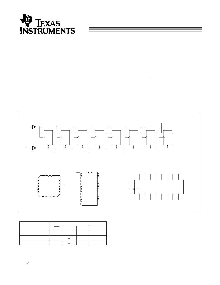
Logic Block Diagram
Pin Configurations
FCT273T1
CP
D
Q
D
0
Q
0
R
D
CP
D
Q
D
1
Q
1
R
D
CP
D
Q
D
2
Q
2
R
D
CP
D
Q
D
3
Q
3
R
D
CP
D
Q
D
4
Q
4
R
D
CP
D
Q
D
5
Q
5
R
D
CP
D
Q
D
6
Q
6
R
D
CP
D
Q
D
7
Q
7
R
D
CP
MR
FCT273T2
4
8
9
10
11
12
7 6 5
1516 17 18
3
2
1
20
13
14
19
D
3
D
2
Q
1
D
6
D
5
D
7
CP
V
CC
GND
Q
5
Top View
D
1
LCC
MR
Q
0
D
0
Q
3
D
4
Q
4
1
2
3
4
5
6
7
8
9
10
11
12
16
17
18
19
20
13
14
V
CC
FCT273T3
15
Top View
Q
6
Q
2
Q
7
Q
0
D
0
D
1
Q
1
Q
2
D
2
D
3
Q
3
D
7
D
6
Q
6
Q
5
D
5
D
4
Q
4
CP
MR
GND
Q
7
DIP/SOIC/QSOP
FCT273T4
CP
MR
D
0
Q
0
D
1
Q
1
D
2
Q
2
D
3
Q
3
D
4
Q
4
D
5
Q
5
D
6
Q
6
D
7
Q
7
Logic Symbol
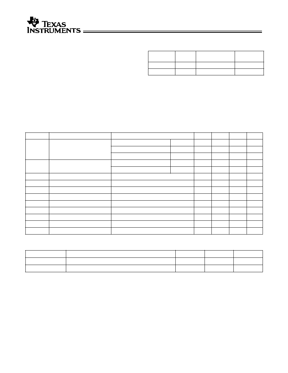
Function Table
[1]
Operating Mode
Inputs
Output
MR
CP
D
Q
Reset (clear)
L
X
X
L
Load `1'
H
h
H
Load `0'
H
l
L
CY54/74FCT273T
2
Maximum Ratings
[2, 3]
(Above which the useful life may be impaired. For user guide-
lines, not tested.)
Storage Temperature
.....................................-
65
°
C to +150
°
C
Ambient Temperature with
Power Applied
..................................................-
65
°
C to +135
°
C
Supply Voltage to Ground Potential
..................-
0.5V to +7.0V
DC Input Voltage
.................................................-
0.5V to +7.0V
DC Output Voltage
..............................................-
0.5V to +7.0V
DC Output Current (Maximum Sink Current/Pin).......120 mA
Power Dissipation ..........................................................0.5W
Static Discharge Voltage............................................>2001V
(per MIL-STD-883, Method 3015)
Operating Range
Range
Range
Ambient
Temperature
V
CC
Commercial
All
40
°
C to +85
°
C
5V
±
5%
Military
[4]
All
55
°
C to +125
°
C
5V
±
10%
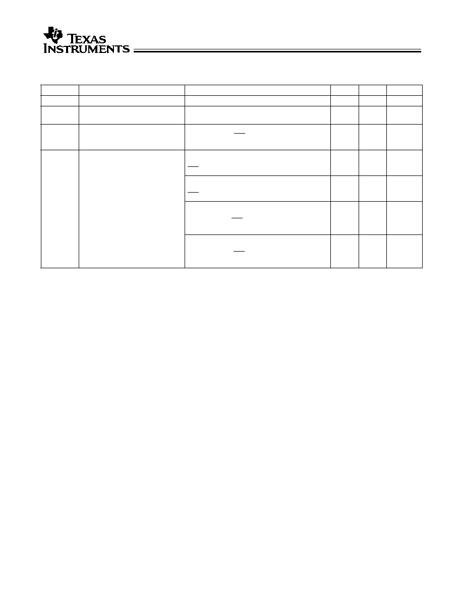
Electrical Characteristics
Over the Operating Range
Parameter
Description
Test Conditions
Min.
Typ.
[5]
Max.
Unit
V
OH
Output HIGH Voltage
V
CC
=Min., I
OH
=32 mA
Com'l
2.0
V
V
CC
=Min., I
OH
=15 mA
Com'l
2.4
3.3
V
V
CC
=Min., I
OH
=12 mA
Mil
2.4
3.3
V
V
OL
Output LOW Voltage
V
CC
=Min., I
OL
=64 mA
Com'l
0.3
0.55
V
V
CC
=Min., I
OL
=32mA
Mil
0.3
0.55
V
V
IH
Input HIGH Voltage
2.0
V
V
IL
Input LOW Voltage
0.8
V
V
H
Hysteresis
[6]
All inputs
0.2
V
V
IK
Input Clamp Diode Voltage
V
CC
=Min., I
IN
=18 mA
0.7
1.2
V
I
I
Input HIGH Current
V
CC
=Max., V
IN
=V
CC
5
µ
A
I
IH
Input HIGH Current
V
CC
=Max., V
IN
=2.7V
±
1
µ
A
I
IL
Input LOW Current
V
CC
=Max., V
IN
=0.5V
±
1
µ
A
I
OS
Output Short Circuit Current
[7]
V
CC
=Max., V
OUT
=0.0V
60
120
225
mA
I
OFF
Power-Off Disable
V
CC
=0V, V
OUT
=4.5V
±
1
µ
A
Capacitance
[6]
Parameter
Description
Typ.
[5]
Max.
Unit
C
IN
Input Capacitance
5
10
pF
C
OUT
Output Capacitance
9
12
pF
Notes:
2.
Unless otherwise noted, these limits are over the operating free-air temperature range.
3.
Unused inputs must always be connected to an appropriate logic voltage level, preferably either V
CC
or ground.
4.
T
A
is the "instant on" case temperature
5.
Typical values are at V
CC
=5.0V, T
A
=+25°C ambient.
6.
This parameter is specified but not tested.
7.
Not more than one output should be shorted at a time. Duration of short should not exceed one second. The use of high-speed test apparatus and/or sample
and hold techniques are preferable in order to minimize internal chip heating and more accurately reflect operational values. Otherwise prolonged shorting of
a high output may raise the chip temperature well above normal and thereby cause invalid readings in other parametric tests. In any sequence of parameter
tests, I
OS
tests should be performed last.
CY54/74FCT273T
3
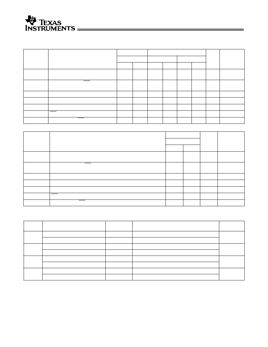
Power Supply Characteristics
Parameter
Description
Test Conditions
Typ.
[5]
Max.
Unit
I
CC
Quiescent Power Supply Current
V
CC
=Max., V
IN
0.2V, V
IN
V
CC
-0.2V
0.1
0.2
mA
I
CC
Quiescent Power Supply Current
(TTL inputs HIGH)
V
CC
=Max., V
IN
=3.4V, f
1
=0, Outputs Open
[8]
0.5
2.0
mA
I
CCD
Dynamic Power Supply Current
[9]
V
CC
=Max., One Bit Toggling, 50% Duty Cycle,
Outputs Open, MR=V
CC
,
V
IN
0.2V or V
IN
V
CC
-0.2V
0.06
0.12
mA/MHz
I
C
Total Power Supply Current
[10]
V
CC
=Max., f
0
=10 MHz, 50% Duty Cycle,
Outputs Open, One Bit Toggling at f
1
=5 MHz,
MR=V
CC
, V
IN
0.2V or V
IN
V
CC
-0.2V
0.7
1.4
mA
V
CC
=Max., f
0
=10 MHz, 50% Duty Cycle,
Outputs Open, One Bit Toggling at f
1
=5 MHz,
MR=V
CC
, V
IN
=3.4V or V
IN
=GND
1.2
3.4
mA
V
CC
=Max., f
0
=10 MHz, 50% Duty Cycle,
Outputs Open, Eight Bits Toggling
at f
1
=2.5MHz, MR=V
CC
,
V
IN
0.2V or V
IN
V
CC
-0.2V
1.6
3.2
[11]
mA
V
CC
=Max., f
0
=10 MHz, 50% Duty Cycle,
Outputs Open, Eight Bits Toggling
at f
1
=2.5 MHz, MR=V
CC
,
V
IN
=3.4V or V
IN
=GND
3.9
12.2
[11]
mA
Notes:
8.
Per TTL driven input (V
IN
=3.4V); all other inputs at V
CC
or GND.
9.
This parameter is not directly testable, but is derived for use in Total Power Supply calculations.
10. I
C
= I
QUIESCENT
+ I
INPUTS
+ I
DYNAMIC
I
C
= I
CC
+
I
CC
D
H
N
T
+I
CCD
(f
0
/2 + f
1
N
1
)
I
CC
= Quiescent Current with CMOS input levels
I
CC
= Power Supply Current for a TTL HIGH input (V
IN
=3.4V)
D
H
= Duty Cycle for TTL inputs HIGH
N
T
= Number of TTL inputs at D
H
I
CCD
= Dynamic Current caused by an input transition pair (HLH or LHL)
f
0
= Clock frequency for registered devices, otherwise zero
f
1
= Input signal frequency
N
1
= Number of inputs changing at f
1
All currents are in milliamps and all frequencies are in megahertz.
11. Values for these conditions are examples of the I
CC
formula. These limits are specified but not tested.
CY54/74FCT273T
4
Document #: 38-00380-A
Switching Characteristics
Over the Operating Range
[12]
Parameter
Description
FCT273T
FCT273AT
Unit
Fig. No.
[13]
Commercial
Military
Commercial
Min.
Max.
Min.
Max.
Min.
Max.
t
PLH
t
PHL
Propagation Delay Clock to Output
2.0
13.0
2.0
8.3
2.0
7.2
ns
1, 5
t
PLH
t
PHL
Propagation Delay MR to Output
2.0
13.0
2.0
8.3
2.0
7.2
ns
1, 6
t
S
Set-Up Time HIGH or LOW D to Clock
2.0
2.0
2.0
ns
4
t
H
Hold Time HIGH or LOW D to Clock
1.5
1.5
1.5
ns
4
t
W
Clock Pulse Width HIGH or LOW
6.0
6.0
6.0
ns
5
t
W
MR Pulse Width LOW
6.0
6.0
6.0
ns
6
t
REC
Recovery Time MR to Clock
2.0
2.5
2.0
ns
6
Parameter
Description
FCT273CT
Unit
Fig. No.
[13]
Commercial
Min.
Max.
t
PLH
t
PHL
Propagation Delay Clock to Output
2.0
5.8
ns
1, 5
t
PLH
t
PHL
Propagation Delay MR to Output
2.0
6.1
ns
1, 6
t
S
Set-Up Time HIGH or LOW D to Clock
2.0
ns
4
t
H
Hold Time HIGH or LOW D to Clock
1.5
ns
4
t
W
Clock Pulse Width HIGH or LOW
6.0
ns
5
t
W
MR Pulse Width LOW
6.0
ns
6
t
REC
Recovery Time MR to Clock
2.0
ns
6
Ordering Information
Speed
(ns)
Ordering Code
Package
Name
Package Type
Operating
Range
5.8
CY74FCT273CTQCT
Q5
20-Lead (150-Mil) QSOP
Commercial
CY74FCT273CTSOC/SOCT
S5
20-Lead (300-Mil) Molded SOIC
7.2
CY74FCT273ATQCT
Q5
20-Lead (150-Mil) QSOP
Commercial
CY74FCT273ATSOC/SOCT
S5
20-Lead (300-Mil) Molded SOIC
8.3
CY54FCT273ATLMB
L61
20-Square Leadless Chip Carrier
Military
CY54FCT273ATDMB
D6
20-Lead (300-Mil) CerDIP
13.0
CY74FCT273TQCT
Q5
20-Lead (150-Mil) QSOP
Commercial
CY74FCT273TSOC/SOCT
S5
20-Lead (300-Mil) Molded SOIC
Notes:
12. Minimum limits are specified but not tested on Propagation Delays.
13. See "Parameter Measurement Information" in the General Information section.
CY54/74FCT273T
5
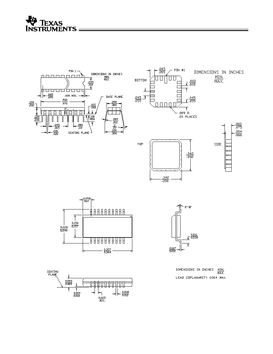
Package Diagrams
20-Lead (300-Mil) CerDIP D6
MIL-STD-1835 D- 8 Config.A
20-Pin Square Leadless Chip Carrier L61
MIL-STD-1835 C-2A
20-Lead Quarter Size Outline Q5