
- 1 -
JULY 22, 1996
SLWS130
This document contains information which may be changed at any time without notice
GC3011 DIGITAL RESAMPLER
1.1
BLOCK DIAGRAM
A block diagram illustrating the major functions of the chip is shown in Figure 1
Figure 1. GC3011 Block Diagram
DOUT[0:11]
12 bits
12 bits
INTERPOLATION FILTER
4096 STEPS
16 SAMPLE
FIFO
INTERPOLATION
CONTROL
CLK IN
OUTPUT CLOCK
GENERATOR
(FIXED CLOCK MODE OR
CLK
OCK
IN
OUT
FE
CKOUT
BYPASS
DATA
ERROR
INTERPOLATION
DIN[0:11]
INTERPOLATION
OUTPUT MUX AND FORMAT
PLL AND VCO)
CONTROL IFACE
A[0:3]
C[0:8]
R/W
CS
TO ALL CIRCUITS
RATIO
MODES
OUTPUT
MODES
OUTPUT
MODES
15 TAPS
INTERPOLATION
RATIO
ERROR
ERROR
AND MODES
INTERPOLATION
RLL
MULTI-CHIP
SYNC
DC[0:11]
CV,FOZ,FIZ
M/S
12 bits
AND OFFSET
DVAL
4 bits
8 bits
CK
SI
SYNC
CIRCUIT
HF
FRST
CK2X
SO
OUT
SI
SO
RESET
CVOUT
CVIN
EIN
EVAL
1.0
KEY FEATURES
�
80 million samples per second (MSPS) input rate
�
Fractional rate change down to 1/4
th
the input rate
�
Synchronization logic to allow multi-chip complex
data operation.
�
Multiple chips can be synchronized with fixed delay
offsets.
�
Two chips allow rate changes up or down.
�
12 bit data I/O
�
32 bit rate control accumulator
�
16 sample output FIFO
�
15 tap linear phase interpolator
�
4096 interpolation steps
�
80% input passband (0 to 0.4F
CK
)
�
+/- 0.1 dB passband ripple
�
Less than +/- 0.02 degrees rms phase jitter
�
-73 dB image rejection
�
60 dB worst case NPR
�
Adaptive rate change to lock the resampling
ratio to the output clock rate
�
PLL/VCO to generate an output clock to
match the rate change
�
Microprocessor interface for control, output,
and diagnostics
�
Built in diagnostics
�
2W power at 50 MHz, 5 volts
�
520 mW at 30 MHz, 3.3 volts
�
100 pin QFP package

GRAYCHIP,INC.
- 2 -
JULY 22, 1996
GC3011 DIGITAL RESAMPLER
This document contains information which may be changed at any time without notice
2.0
FUNCTIONAL DESCRIPTION
Fabricated in 0.7 micron CMOS technology, the GC3011 chip is a general purpose digital resampler
chip designed to accurately reduce the sample rate of the input data stream by a fractional amount ranging
from 1.0 down to 0.25. The chip includes an interpolation control block, a multi-chip synchronization and
offset circuit, a 15 tap interpolation filter, a 16 word output FIFO memory, an output clock generator and an
interpolation ratio rate-lock loop (RLL) circuit. In addition, an output multiplexor circuit allows the user to
by-pass the FIFO and output the resampled samples directly. A control interface allows the user to set the
resampling modes, resampling rate and output clocking modes.
The multi-chip sync and offset circuit allows multiple GC3011 chips to be synchronized in a
master/slave configuration. The offset portion of the circuit allows each chip's interpolation delay to be offset
by a fixed amount relative to the other chips. The GC3011 chip accepts input rates up to 70 MHz.
The chip can operate in a fixed resampling mode where the user specifies the desired output rate,
or the chip can be configured to adapt the resampled rate to match an externally provided output clock. The
resampled data can be output synchronous to the input clock or can be output synchronous to the output
clock. When output synchronous to the input clock the samples are accompanied by a data valid flag to
indicate which samples are valid and which are invalid. When output synchronous to the output clock the
chip uses the internal 16 word FIFO to smooth the data. The output clock can be provided externally, or can
be generated within the chip using the internal oscillator which is locked to the resampled data rate.
The chip does not provide any anti-alias filtering. The user must bandlimit the input signal before it
is down-sampled by the GC3011 chip. The GC2011 digital filter chip can be used for this purpose.
Fractional upsampling can be achieved by using the GC2011 digital filter chip to up sample the
signal by a factor of two before it is downsampled by the GC3011.
On chip diagnostic circuits are provided to simplify system debug and maintenance.
The chip receives configuration and control information over a microprocessor compatible bus
consisting of an 8 bit data I/O port, a 4 bit address port, a read/write bit, and a control select strobe. The
chip's 16 control registers (8 bits each) are memory mapped into the 4 bit address space of the control port.
2.1
CONTROL INTERFACE
The chip is configured by writing control information into sixteen control registers within the chip.
The contents of these control registers and how to use them are described in Section 4.0. The registers are
written to or read from using the
C[0:7]
,
A[0:3]
,
R/W
, and
CS
pins. Each control register has been assigned
a unique address within the chip. An external processor (a microprocessor, computer, or DSP chip) can
write into a register by setting
A[0:3]
to the desired register address, setting the
R/W
pin low, setting
C[0:7]
to the desired value and then pulsing
CS
low.
To read from a control register the processor must set
A[0:3]
to the desired address, set
R/W
high,
and then set
CS
low. The chip will then drive
C[0:7]
with the contents of the selected register. After the
processor has read the value from
C[0:7]
it should set
CS
high. The
C[0:8]
pins are turned off (high

GRAYCHIP,INC.
- 3 -
JULY 22, 1996
GC3011 DIGITAL RESAMPLER
This document contains information which may be changed at any time without notice
impedance) whenever
CS
is high or
R/W
is low. The chip will only drive these pins when
CS
is low and
R/W
is high.
2.2
SYNC CIRCUIT
The sync circuit is used to synchronize the chip during diagnostics or system initialization. The sync
circuit includes a 20 bit counter which can be programmed to generate terminal count (TC) sync pulses
every 2
8
, 2
12
, 2
16
or 2
20
input clock cycles. The counter can be synchronized to the SI sync input, or left to
free run. The SI and TC sync pulses can be used to synchronize or clear the counters, accumulators or state
machines found within the rest of the chip. The lower 12 bits of the counter are used as input samples to
the resampler during diagnostics.
The user may select which sync signal is output from the chip on the SO pin. The SO signal can be
either a delayed version of the sync input, the counter's TC sync, or a one-shot pulse. The sync output signal
is one clock cycle wide, synchronized to the output clock (OCK).
2.3
INTERPOLATION FILTER
The interpolation filter is used to interpolate between input data samples in order to generate output
samples at fractional time delays relative to the input samples. The filter is a 15 tap FIR filter with 4096 sets
of coefficients. Each set of coefficients corresponds to a different time delay between input samples. The
circuit accepts a new delay control word (12 bits) every clock cycle which tells it which set of coefficients to
use during that clock cycle. This allows the interpolation time delays to vary every clock sample.
Interpolating to 4096 delay values gives a worst case phase error (phase jitter) of +/- 360/8192 = +/- 0.09
degrees.
The delay control word can either come from the interpolation control circuit described below, or
from an external source. The external input allows multiple resamplers to be synchronized to controls
coming from a common resampler chip in a master/slave arrangement.
2.4
INTERPOLATION CONTROL
The interpolation control circuit is used to generate the time delay control words used by the
interpolation filter. The interpolated output rate is specified as the ratio of the input rate to the output rate.
This ratio is limited to be within the range of 1 to 4 and is formatted as a 32 bit word. The most significant 2
bits are the integer portion of the ratio and the lower thirty bits are the fractional part. This ratio is equivalent
to the ratio of the output sample spacing to the input sample spacing. The interpolation ratio feeds a 32 bit
accumulator. The 2 bit integer portion of the accumulator's output is used to determine the number of input
samples to skip between output samples, and the upper 12 bits of the fractional part is used as the
interpolation filter's delay control word.
GRAYCHIP,INC.
- 4 -
JULY 22, 1996
GC3011 DIGITAL RESAMPLER
This document contains information which may be changed at any time without notice
2.5
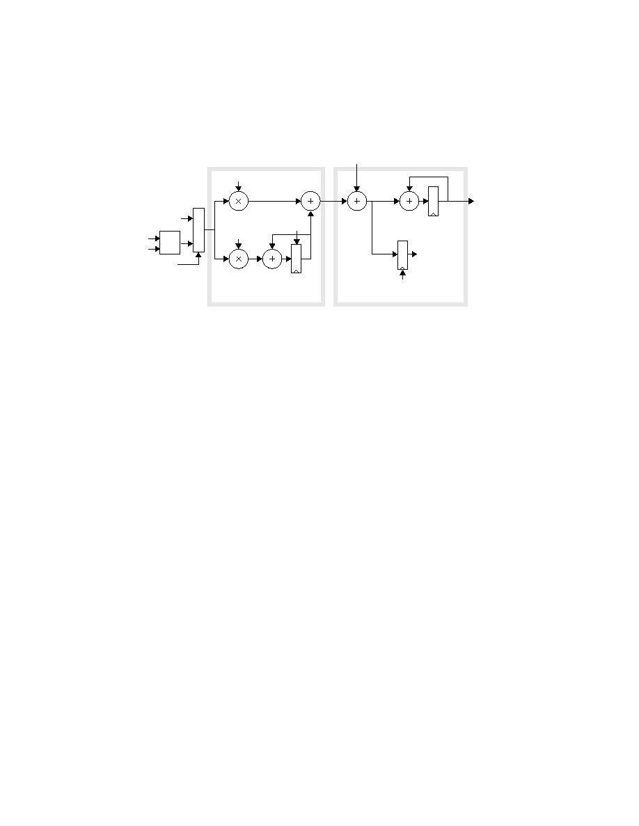
INTERPOLATION RLL
The interpolation ratio can be fixed by the user, or can be allowed to adapt to the ratio that keeps
the output FIFO half-full. The adaption is performed by the interpolation rate lock loop (RLL) circuit. Figure
2 is a block diagram showing the interpolation RLL circuit and the interpolation control circuit.
Figure 2. Interpolation RLL And Control Circuits
2.5.1
Fixed Interpolation Mode
The fixed interpolation mode is used when the user knows what the desired output rate should be
relative to the input rate. For example, a user may wish to use this mode when he is using the resampler to
baud synchronize a modem signal. In this case the user has an external baud rate detection circuit which
tells the user how to adjust the interpolation ratio.
The user fixes the interpolation ratio by turning off (clearing) the Rate-Locked-Loop (RLL) circuit.
Clearing the RLL output fixes the delay accumulator's input to be the 32 bit value supplied by the user.
2.5.2
Adaptive Interpolation Mode
In this mode the RLL circuit automatically adjusts the interpolation ratio to keep the FIFO half full.
This mode is used when the output clock is fixed and the chip's interpolation ratio must exactly match the
ratio between the chip's input clock and the output clock. For example, a user may wish to use the adaptive
interpolation mode in order to interface two asynchronous signal processing systems, or when an external
baud sync circuit has provided a baud synchronous output clock.
The adaption uses an error signal from the FIFO. The error is a bit indicating the error is plus or
minus one. A minus one indicates that the FIFO is less than half full and the interpolation ratio (the ratio of
the input rate to the output rate) needs to be decreased. A plus one indicates that the FIFO is more than
half full and the interpolation ratio needs to be increased. The user sets up the adaptive interpolation mode
2
-A
OR CLEAR
2
-B
OR CLEAR
ERROR
FROM
FIFO
RATE-LOCKED-LOOP
INTERPOLATION
DELAY
CONTROL
WORD
(12 BITS)
CLEAR
DELAY ACCUMULATOR
32 bits
32 bits
RATIO
RATIO_HOLD
TO
CONTROL
INTERFACE
16 MSBs
32 bits
INTERPOLATION CONTROL
MUX
EXT_ERR
EIN
EVAL
ERROR
LATCH

GRAYCHIP,INC.
- 5 -
JULY 22, 1996
GC3011 DIGITAL RESAMPLER
This document contains information which may be changed at any time without notice
by setting the interpolation ratio to a value close to the actual ratio
1
and setting the adaption constants 2
-A
and 2
-B
, where A and B are constants ranging from 0 to 31.
These constants set the adaption rate and the tracking bandwidth of the adaption loop. These
constants can also be set to zero in order to clear the 2
-A
or 2
-B
feedback paths or to freeze the adaption
process. A large value for B will slow the adaption process and will reduce the phase jitter, but will also
decrease the tracking bandwidth of the loop. The adaption time when the interpolation ratio starts at zero
will be approximately 2
B
clock cycles. The tracking bandwidth of the loop is determined by how fast the loop
will adapt to an output rate change and if it adapts fast enough to prevent a FIFO overflow or underflow error.
Since the FIFO has a range of +/- 8 samples, the tracking range in Hz is approximately 2
(3-B)
times the input
clock rate
2
.
The constant 2
-A
is used to dampen the adaption loop to prevent ringing. The value of A should be
approximately one-half of B. Note that small values of A will introduce residual phase jitter equal to +/-
360x2
-A
degrees.
The values of A and B are application dependant. If adaption time is important, then a two-stage
adaption process may be desirable. An initial setting of B equal to 16 and A equal to 12 will allow the loop
to converge rapidly. Once the loop has converged, A and B can be set to minimize residual phase noise.
Settings between 22 and 31 for B and between 14 and 15 for A are suggested. A setting of B=22 gives a
tracking bandwidth of 128 Hz. A setting of B=31 would reduce the tracking bandwidth to about 0.25 Hz.
2.5.3
External Adaption Mode
The RLL can be adapted from an external error signal using the EIN and EVAL inputs to the chip.
In this mode the user uses an external circuit to detect resampling rate errors and drives the EIN with a 0
or a 1. A `1' means increase the ratio and a`0' means decrease it. A high level on the EVAL signal identifies
when the EIN signal is valid. The EVAL and EIN signals are clocked into the chip on the rising edge of the
input clock.
2.5.4
The Ratio-Hold Register
The user can monitor current resampling ratio using the Ratio-Hold Register. This register captures
and holds the most significant 16 bits of the current resampling ratio when the RATIO_HOLD bit is set (See
Section 4.8). This register can be used to determine if the resampler has converged in the adaptive
interpolation mode (See Section 2.5.2 above).
1. This speeds up the adaption, but is not necessary for the adaption to work. The ratio can be set to zero if desired.
2. The chip will converge to the correct interpolation ratio outside of the tracking bandwidth, but while it is converging
the FIFO will overflow or underflow so that the data output will be corrupted until it re-converges.