 | –≠–ª–µ–∫—Ç—Ä–æ–Ω–Ω—ã–π –∫–æ–º–ø–æ–Ω–µ–Ω—Ç: GC5018 | –°–∫–∞—á–∞—Ç—å:  PDF PDF  ZIP ZIP |

www.ti.com
PRODUCT PREVIEW
1
Introduction
1.1
FEATURES
1.2
APPLICATIONS
GC5018
8-CHANNEL WIDEBAND RECEIVER
SLWS169 ≠ MAY 2005
≠
115 dB SFDR NCO
∑
Four 16-Bit CMOS ADC Input Ports
≠
UMTS Mode Rx Filtering: 6 Stage CIC (m=1
∑
Programmable Closed Loop VGA Control With
or 2), Up to 40 Tap CFIR, Up to 64 Tap PFIR
6-Bit Outputs for Each ADC Input Port
≠
CDMA Mode Rx Filtering: 6 Stage CIC (m=1
∑
Provide Received Total Wide Band Power
or 2), Up to 64 Tap CFIR, Up to 64 Tap PFIR
(RTWP) Measurement for the Composite
≠
Power Measurements
Power Across Carriers With Programmable
≠
Final AGC
Time Window for Measurement
∑
1.5V Digital Core Supply, 3.3V Digital I/O
∑
8 UMTS Digital Down Converter (DDC)
Supply
Channels or 16 CDMA or 16 TD-SCDMA DDC
∑
305 Ball Plastic BGA (19 mm x 19 mm) With
Channels With Programmable 18 Bit Filter
1,0 mm Pitch
Coefficients
∑
Power Dissipation: ~2W
∑
Each DDC channel includes
≠
Real or Complex DDC Inputs
∑
Wireless Base Station Receiver
∑
Multi-Carrier Digital Receiver
∑
UMTS (4 Carriers-1 Sector With Diversity)
∑
CDMA (8 Carriers-1 Sector With Diversity)
∑
TD-SCDMA (16 Carriers-1 Sector Without
Diversity, 8 Carriers-1-Sector With Diversity)
∑
Digital Radio Receivers
∑
Wide Band Receivers
∑
Software Radios
∑
Wireless Local Loop
∑
Intelligent Antenna Systems
Please be aware that an important notice concerning availability, standard warranty, and use in critical applications of Texas
Instruments semiconductor products and disclaimers thereto appears at the end of this document.
PRODUCT PREVIEW information concerns products in the forma-
Copyright © 2005, Texas Instruments Incorporated
tive or design phase of development. Characteristic data and other
specifications are design goals. Texas Instruments reserves the
right to change or discontinue these products without notice.
www.ti.com
PRODUCT PREVIEW
Contents
2
General Description
GC5018
8-CHANNEL WIDEBAND RECEIVER
SLWS169 ≠ MAY 2005
1
Introduction
...............................................
1
5.1
Digital Receive Section Signals
....................
105
1.1
FEATURES
...........................................
1
5.2
Microprocessor Signals
............................
108
1.2
APPLICATIONS
......................................
1
5.3
JTAG Signals
......................................
109
2
General Description
.....................................
2
5.4
Factory Test and No Connect Signals
.............
109
3
RECEIVE DIGITAL SIGNAL PROCESSING
.........
3
5.5
Power and Ground Signals
........................
110
3.1
Receive Input Interface
...............................
4
5.6
Digital Supply Monitoring
..........................
110
3.2
DDC Organization
...................................
15
5.7
JTAG
...............................................
110
4
GC5018 GENERAL CONTROL
.......................
42
6
SPECIFICATIONS
.....................................
111
4.1
Microprocessor Interface Control Data, Address,
6.1
ABSOLUTE MAXIMUM RATINGS
.................
111
and Strobes
.........................................
43
6.2
RECOMMENDED OPERATING CONDITIONS
...
111
4.2
Synchronization Signals
.............................
45
6.3
THERMAL CHARACTERISTICS
..................
111
4.3
Interrupt Handling
...................................
46
6.4
DC CHARACTERISTICS
..........................
112
4.4
GC5018 Programming
..............................
47
6.5
AC TIMING CHARACTERISTICS
.................
112
5
GC5018 PINS
...........................................
105
The GC5018 is a multi-channel communications signal processor that provides digital downconversion
optimized for cellular base transceiver systems. The device supports UMTS, CDMA-1X and TD-SCDMA
air interface cellular standards.
The chip provides up to 8 UMTS digital downconverter channels (DDC), 16 CDMA DDCs or 16
TD-SCDMA DDCs. The DDC channels are independent and operate simultaneously.
The GC5018 has four 16-bit inputs. Each DDC channel can be programmed to accept data from any one
(or two for complex input mode) of the four input ports.
2
Contents
www.ti.com
PRODUCT PREVIEW
I
sync
DDC0
2 CDMA2000-1X,
2 TD-SCDMA or 1 UMTS
Q
16
rxin_a
adcclk_a
16
rxin_b
adcclk_b
Digital receive
data ports
JTAG
tdo
trst_n
tck
tdi
tms
Control and Sync
d(15:0)
16
a(5:0)
6
rd_n wr_n ce_n
rx_sync a-d
4
reset_n
interrupt
rx_sync_out
rxclk
6
6
6
6
dvga_a
dvga_b
dvga_c
dvga_d
Receive Input
Interface
Power
Measurements and
WidebandAGC
DDC1
2 CDMA2000-1X,
2 TD-SCDMA or 1 UMTS
DDC2
2 CDMA2000-1X,
2 TD-SCDMA or 1 UMTS
DDC3
2 CDMA2000-1X,
2 TD-SCDMA or 1 UMTS
DDC5
2 CDMA2000-1X,
2 TD-SCDMA or 1 UMTS
DDC4
2 CDMA2000-1X,
2 TD-SCDMA or 1 UMTS
16
rxin_c
adcclk_c
16
rxin_d
adcclk_d
DDC7
2 CDMA2000-1X,
2 TD-SCDMA or 1 UMTS
DDC6
2 CDMA2000-1X,
2 TD-SCDMA or 1 UMTS
I
sync
Q
I
sync
Q
I
sync
Q
I
sync
Q
I
sync
Q
I
sync
Q
I
sync
Q
Output
Format
Parallel
or Serial
rxout_X_X
rx_sync_out_X
32
8
rxclk_out
3
RECEIVE DIGITAL SIGNAL PROCESSING
GC5018
8-CHANNEL WIDEBAND RECEIVER
SLWS169 ≠ MAY 2005
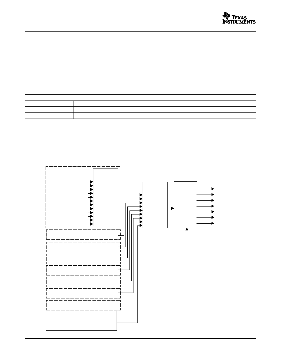
The down conversion section of the GC5018 consists of the receive input interface, the rx_distribution
bus, and 8 digital downconverter blocks.
The purpose of the receive input interface is to accept signal data from four 16 bit input ports, measure the
input signal power, control the digital VGA and to distribute the data to the DDC blocks. The input
interface also has a user-controlled test generator and noise source.
The rx_distribution bus distributes the four channels of signal data to each of the 8 DDC blocks.
Each DDC block selects one of the four channels (or 2 for complex input data) from the rx_distribution bus
and then performs downconversion tuning, programmable delay, channel filtering with decimation, power
measurement, fixed gain adjust and/or automatic gain control. Each DDC block can support 1 UMTS
channel, 2 CDMA channels or 2 TD-SCDMA channels. An optional mode permits stacking two DDC
blocks in UMTS mode to provide double-length final pulse shaping filtering.
Tuned, filtered, and decimated signal data is output in bit serial or parallel format.
RECEIVE DIGITAL SIGNAL PROCESSING
3

www.ti.com
PRODUCT PREVIEW
3.1
Receive Input Interface
FIFO
16
rxin _a
16
dual real or
single complex
Power Meter
FIFO
16
rxin _b
16
FIFO
16
rxin _c
16
FIFO
16
rxin _d
16
dual real or
single complex
Power Meter
dual real or
single complex
AGC
dual real or
single complex
AGC
dvga_c
dvga_d
dvga_a
dvga_b
6
6
6
6
18
rx_distribution
bus to DDC
channels
test & noise
signal
generator
16
16
16
16
test & noise
signal
generator
test & noise
signal
generator
test & noise
signal
generator
to testbus
test bus select
and decimation
testbus
sources
1 to 64
sample
delay
line
delay_a
18
1 to 64
sample
delay
line
delay_b
18
1 to 64
sample
delay
line
delay_c
18
1 to 64
sample
delay
line
delay_d
GC5018
8-CHANNEL WIDEBAND RECEIVER
SLWS169 ≠ MAY 2005
The GC5018's receive input data interface accepts data from two sources:
∑
Signal data presented at the four 16-bit digital data input ports.
∑
A LFSR test signal generator allows the GC5018 to be tested using a known repetitive data sequence.
Signal data can be provided in binary or 2's complement form. The location of the ADC's MSB can be
programmed to allow for additional AGC headroom if desired. For example, a 14-bit ADC may be
connected with the MSBs aligned, or shifted down to allow the AGC additional gain range before clipping
the signal.
Signal data can be accepted at rates up to rxclk in UMTS mode for either 8 normal channels or 4 double
length final pulse shaping filter channels. In CDMA mode the maximum input rate is rxclk for real inputs, or
rxclk/2 for complex inputs. For maximum filter performance, higher clock rates generally allow longer
filters.
Complex signal data is input with I data driving one input port and Q data driving another. This means that
there are only two signal data ports available when using complex input mode. The mapping of I and Q
data onto the four input ports is programmable.
Signal input data is clocked into 8-stage FIFOs using a matching external clock signal adcclk_a/b/c/d.
Signal data is clocked out of the FIFO from a gated rxclk (the GC5018 receive section clock). The FIFO
allows arbitrary phase relationship between adcclk_a/b/c/d and rxclk. The frequency relationship is
mandated by the programmed configuration.
The test and noise generator can supply test sequences or add noise to the input signal data. The test
sequences, when combined with the checksum generators, are useful for initial board debug or power-on
self-test.
For applications that require receiver desensitization, the noise generator can add noise to input data
streams.
Many internal chip signals can be routed to the testbus for evaluation and debug purposes. When the
testbus is enabled, the rxin_c and rxin_d ports are driven as digital outputs.
4
RECEIVE DIGITAL SIGNAL PROCESSING

www.ti.com
PRODUCT PREVIEW
3.1.1
Receive FIFO
GC5018
8-CHANNEL WIDEBAND RECEIVER
SLWS169 ≠ MAY 2005
Each of the four outputs to the DDC channels includes a 1 to 64 sample delay line.
PROGRAMMING
VARIABLE
DESCRIPTION
ssel_ddc(2:0)
Selects the sync source for the DDC data input mux and mixer. This sets the sync source for DDC input clock
generation and synchronization for all DDC channels.
offset_bin_X
Selects offset binary input when set, 2's complement input when cleared. X={a,b,c,d}
msb_pos_X(2:0)
Identifies the connection location of the ADC's MSB. Programmed values of {0..7} corresponds to msb at {rxin_x_15..
rxin_x_8}. X={a,b,c,d}
The receive FIFO consists of an 8 stage memory and 2 counters generating the input write pointer and
output read pointer. When the FIFO receives a sync signal, the input and output pointers are initialized
with a write to read pointer offset of four samples. Input samples from rxin_X (writes) are clocked with the
adcclk_X input clock rising edges, and the input pointer advances on each clock rising edge. Output
samples (reads) and the output pointer are clocked with the rxclk input signal rising edges, divided by the
programmed sample rate loaded into the rate_sel(1:0) control register.
PROGRAMMING
VARIABLE
DESCRIPTION
adc_fifo_bypass
When set, bypasses the input FIFOs and input data is latched directly using the rxclk. When cleared, input data is
latched using the adcclk_a/b/c/d inputs.
ssel_adc_fifo(2:0)
Selects the sync source for the FIFO state machines. This sync signal initializes the FIFO input and output
pointers.
rate_sel(1:0)
This selects the FIFO input and output rate; {rxclk, rxclk/2, rxclk/4 or rxclk/8 }. For example, with rxclk at
153.6MHz, set rate_sel to 0, 1, 2 or 3 respectively for adcclk_a/b/c/d 153.6, 76.8, 38.4 or 19.2MHz.
adc_fifo_strap_ab
When set, the rxin_a and rxin_b FIFO input and output pointers are synchronized to support complex input
signals.
adc_fifo_strap_cd
When set, the rxin_c and rxin_d FIFO input and output pointers are synchronized to support complex input
signals.
RECEIVE DIGITAL SIGNAL PROCESSING
5

www.ti.com
PRODUCT PREVIEW
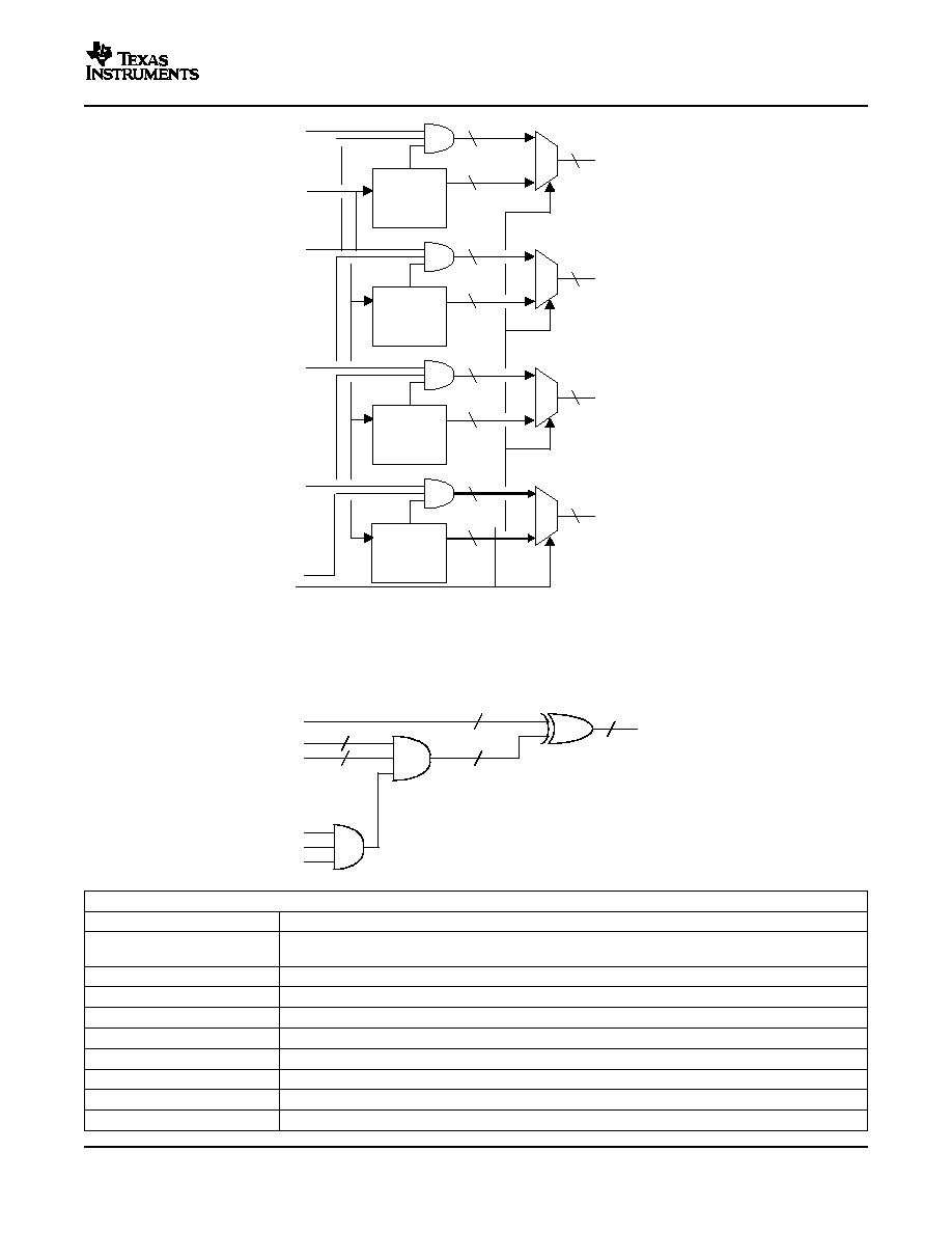
3.1.2
Receive Input Power Meters
from rxin_a FIFO output
from rxin_b FIFO output
pmeter_iq0
pmeter_iq1
from rxin_c FIFO output
from rxin_d FIFO output
pmeter_iq2
pmeter_iq3
I
I
Q
Q
from rxin_a
from rxin_b
power meter 0 results
power meter 1 results
power meter 0
power meter 1
I
I
Q
Q
from rxin_c
from rxin_d
power meter 2 results
power meter 3 results
power meter 2
power meter 3
GC5018
8-CHANNEL WIDEBAND RECEIVER
SLWS169 ≠ MAY 2005
Four Receive Input RMS power meters are provided. For real inputs, the four power meters can be used
to measure the RMS power of the combined carriers in each of the four input signals (the Q input is held
at zero). For complex inputs, two power meters can be use to measure the combined complex power and
two can be disabled.
6
RECEIVE DIGITAL SIGNAL PROCESSING
www.ti.com
PRODUCT PREVIEW
21-bit
integration
counter
clear
sync
delay
sync
event
58-bit
Integrator
58-bit
Register
9-bit
sync delay
counter
21-bit
interval
counter
transfer
sync
delay
(in 8 sample
increments)
integration
(in 8 sample
increments)
21
21
9
RMS power
I
Q
33
32
16
integration time
interval time
integration
start
integration
start
integration
start
interval
(in 8 sample
increments)
16
32
integration time
integration time
GC5018
8-CHANNEL WIDEBAND RECEIVER
SLWS169 ≠ MAY 2005
Power is calculated by squaring each 18 bit I (I and Q for complex inputs) sample, summing, and then
integrating the summed-squared results into a 58 bit accumulator over a programmable integration period.
The integration period is programmed into the 21 bit counter, in 8 sample increments. The power read is:
power = [ (I
2
) x (Xx8 + 1) ] for real inputs where X is the integration count.
power = [ (I
2
+ Q
2
)x (Xx8 + 1) ] for complex inputs where X is the integration count.
A programmable 21 bit interval counter sets the power measurement interval (how often power will be
measured) in 8 sample increments. A measurement integration period is started at the beginning of each
interval period.
The process begins with a sync event starting the 9 bit delay counter. After (8xsync_delay + 2) samples,
the integration interval is started. Integration continues until the integration count is met, at which point the
58 bit integrator results are transferred to the read only register and an interrupt is generated. A new
measurement period will start at the end of the interval period.
NOTE
Each of the four composite RMS power meter blocks has its own delay sync, interval, and
integration period counters, as well as separate sync source registers.
The 21-bit counters in 8 sample increments allow up to 104.8mS interval times at 160MHz clock.
RECEIVE DIGITAL SIGNAL PROCESSING
7

www.ti.com
PRODUCT PREVIEW
3.1.3
Receive Input AGC (RAGC)
freeze control register bit
freeze from sync source
clear control register bit
clear sync source
Map
Table
MSBs
Gain
Map
Table
16
Filter
update
Map
Table
7
1
0
16
8
clip_hi_thresh
clip_low_thresh
clip detect controls
delay adjust
sd_thresh
signal detect
mode controls
128w x 8b ram
update
sync
sync
delay
Samples
from
ADC FIFO
integrate and dump signal power measurement
5
enable corner
no_signal
err_shift 5
32
55
acc_shift
limit
6
31
16
7
{127..0}
-
+
DVGA
Map
Table
6
Gain
Map
Table
6
Highpass
Filter
X2
Error
Map
Table
7
0
Mag
Clip
Detect
clip_error
16
Signal
64w x 22b RAM
update interval
loop accumulator
to DVGA
pins
to DDC
channels
acc_shift
5
shift
&
limit
16
Delay
acc_offset
7
limit
{127..0}
-
+
16
16
Level
Detect
error
shift
GC5018
8-CHANNEL WIDEBAND RECEIVER
SLWS169 ≠ MAY 2005
PROGRAMMING
VARIABLE
DESCRIPTION
recv_pmeterX (57:0)
58 bit power measurement result. X= {0,1,2,3}.
recv_pmeterX_sqr_sum(20:0)
21 bit integration (square and sum) period. X= {0,1,2,3}.
recv_pmeterX_sync_delay(8:0)
Power meter delay sync period. X= {0,1,2,3}.
recv_pmeterX_strt_intrvl(20:0)
21 bit measurement interval. X= {0,1,2,3}. The strt_intrvl value must be greater than the sqr_sum value.
ssel_recv_pmeter_X(2:0)
Sync source. X= {0,1,2,3}.
pmeterX_iq
Selects complex power measurement input mode when set. X= {0,1,2,3}.
recv_pmeterX_ena
Enables power meter when set. X= {0,1,2,3}.
Input signals from the ADCs can be used to create a front end composite AGC loop when combined with
a digitally controlled variable gain amplifier (DVGA) connected before the ADCs. The AGC system
operates by integrating the square of the ADC samples over a programmable interval and applying a table
driven error signal to a loop integrator based on the squared integration output. The error table maps the
signal power to a user programmed error value. The loop integrator output is used to drive map tables to
control the DVGA output pins and a gain adjustment multiplier. Fast updates can be enabled if desired, to
cause the loop integrator to quickly adjust to interfering signals. The ADC input signals can also be passed
through a high pass filter to remove DC offset before squaring the input.
The programmable error table, integrator mapping tables, and clip thresholds, when combined with the
user programmable interval timers provide a highly flexible AGC function.
8
RECEIVE DIGITAL SIGNAL PROCESSING

www.ti.com
PRODUCT PREVIEW
GC5018
8-CHANNEL WIDEBAND RECEIVER
SLWS169 ≠ MAY 2005
The AGC measurement interval timer is a 24-bit timer initialized by a sync after a programmable 8-bit
delay. During the integration interval, the squared input signal is shifted by the programmed value and
accumulated. At the end of the interval time, an update pulse is generated, and the selected 7 bits of the
55-bit accumulated power is upper limit checked and transferred to the power holding register. A
programmable offset is applied, and the following limit check produces a 7 bit address value for the error
map table RAM. The user programmable error map table and following gain shift setting are used to
determine the loop error signal to be added to the 32-bit AGC loop accumulator. The error value is only
added to the loop accumulator once per update. The loop accumulator upper 6 MSBs are used as the
address for the programmable DVGA map table and gain map table. The gain map table address can be
delayed from 0 to 31 clock cycles to align DVGA changes to signal level changes at the output of the
AGC.
The AGC includes four sources for freezing the loop and holding the loop accumulator constant. A general
sync source can be used to directly control the freeze; when the selected sync source is high, the AGC
will be held, and when low, the AGC will operate. A control register bit freezes the AGC in the same
fashion; when the bit is set, the AGC is held, and when cleared, the AGC will operate. A signal level
detector is provided that can be used to automatically freeze the AGC loop in the event of input signal
loss. A programmable signal detection threshold value, number of samples below the signal detection
threshold, and window timer are used to determine when no signal is present. Finally, a programmable
number of AGC updates after sync can be programmed, and the AGC will he held until the next sync
event. Freeze holds the loop accumulator constant, the integrate and dump accumulator constant and the
interval timer constant. When freeze is released, the interval timer will resume counting.
A sync event will always reinitialize the integrate and dump interval timer, and terminate the pending
update to the loop accumulator from the current integrate and dump measurement interval. For example, if
a sync event occurs during an integrate and dump interval, that interval will be terminated without updating
the loop, and the integrate and dump accumulator will be cleared. After the programmed sync delay, a
new interval will start.
The AGC includes a dual threshold clip detect function, using two programmable 16-bit thresholds and
programmable counters. The clip detector will cause immediate loop accumulator updates while the clip
event is active. The 16-bit clip error value is aligned at the MSBs of the loop accumulator. Clip events are
qualified when a programmed number of samples are above the high clip threshold during the
programmable clip window time. For example, a clip event can be defined as 8 samples above the clip
high threshold in a 256 sample window; the clip high threshold, the number of samples above the high clip
threshold and the sample window time are programmable. Once the clip event has occurred, the clip
duration is controlled by the clip low threshold value, clip low samples value and clip low timer. The clip
event is cleared when the number of samples below the low clip threshold exceeds the programmed value
within the clip low timer window. The clip low threshold, number of clip low samples and the clip low
window timer are programmable.
The AGC blocks can be paired together, rxin_a with rxin_b, and rxin_c with rxin_d, to produce a complex
input AGC mode. The clip detector output from the rxin_b/d AGCs is logically OR'ed with the rxin_a/c clip
detect outputs. The squared input function before the integrate and dump and signal level detector is
replaced with a I
2
+ Q
2
power calculation. The accumulator MSBs from the rxin_a/c AGCs are connected
to the rxin_c/d DVGA map table and gain map table inputs. This arrangement allows the AGCs to operate
in a direct conversion receiver system by controlling the I
2
+ Q
2
complex signal level.
The highpass filter is a 32 bit accumulator followed by an adjustable shift to control the corner frequency,
a subtractor to remove the accumulated offset and a final limiter to produce a 16 bit result. The highpass
filter function is enabled by setting hp_ena; clearing hp_ena holds the accumulator reset.
RECEIVE DIGITAL SIGNAL PROCESSING
9

www.ti.com
PRODUCT PREVIEW
17
32
hp_corner
3
shift
&
limit
16
16
limit
-
+
16
17
Samples
from
ADC FIFO
Samples to
X 2 block
hp_ena
GC5018
8-CHANNEL WIDEBAND RECEIVER
SLWS169 ≠ MAY 2005
PROGRAMMING
VARIABLE
DESCRIPTION
ragc_bypass_X
Bypasses the entire receive AGC circuit when set. X = {0,1,2,3}
hp_ena_X
Enables high pass filter when set
hp_corner_X(2:0)
Adjusts the corner frequency of the high pass filter
integ_interval_X(23:0)
Integrate and dump signal power measurement interval in samples.
acc_shift_X(4:0)
Shift down amount following the integrate and dump accumulator.
acc_offset_X(5:0)
Offset value applied to the shifted integrate and dump output.
ragc_sync_delay_X(7:0)
AGC sync delay interval, from 1 to 256 samples.
ssel_ragc_interval_X(2:0)
Sync source selection for the interval timer.
ssel_ragc_freeze_X(2:0)
Sync source selection for AGC freeze
ssel_ragc_clear_X(2:0)
Sync source selection for the AGC loop accumulator clear
ragc_freeze_X
Register bit to freeze the AGC when set
ragc_clear_X
Register bit to clear the AGC accumulator when set
ragc_update_X(7:0)
Sets the number of updates per sync event, after which no further updates will occur until the next sync
event. Program to 0x00 to continually update.
sd_ena_X
Enables freezing the AGC with the signal detector when set
sd_thresh_X(15:0)
Signal detection threshold for AGC channel X. This 16 bit word is lined up with bits 23 down to 8 of the
square output. The smallest signal level is that can be programmed is therefor 16 LSBs on the ADC
input, and the largest is 4095 LSBs at the ADC input.
sd_samples_X(15:0)
The number of samples below the signal detect threshold within the signal detect sample timer window
required to freeze on the AGC.
sd _timer_X(15:0)
Window timer to qualify signal detection.
clip_hi_thresh_X(15:0)
Clip detector high threshold
clip_lo_thresh_X(15:0)
Clip detector low threshold
clip_hi_samples_X(7:0)
A clip event is detected when this number of samples above the clip high threshold within the clip high
sample timer window exceeds this value.
clip_lo_samples_X(7:0)
A clip event ends when this number of samples below the clip low threshold within the clip low sample
timer window exceeds this value.
clip_hi_timer_X(15:0)
Window timer to qualify clip events.
clip_lo_timer_X(15:0)
Window timer to determine when the clip event ends.
clip_error_X(15:0)
Error signal applied to the AGC accumulator when a clip event is active. This data is MSB aligned, and
therefor can cause immediate changes to the accumulator.
ragc_error_map_X
128w x 8b memory holding the log to error look up table.
dvga_map_X
64w x 6b memory holding the accumulator to DVGA look up table
gain_map_X
64w x 16b memory holding the accumulator to GAIN look up table (256 decibels is unity gain).
delay_adj_X(4:0)
Delay between DVGA output updates and gain map updates to compensate for ADC pipeline delays,
etc.
err_shift_X(4:0)
Error map table output shift up before adding to loop accumulator
complex_01
Enables complex AGC mode on inputs rxin_a and rxin_b when set
complex_23
Enables complex AGC mode on inputs rxin_c and rxin_d when set
10
RECEIVE DIGITAL SIGNAL PROCESSING
www.ti.com
PRODUCT PREVIEW
3.1.4
Test and Noise Signal Generator
LFSR
0
5
22
initialized on sync event - each of the four generators has a different seed
adcclk_X
sync
lfsr(22:0)
GC5018
8-CHANNEL WIDEBAND RECEIVER
SLWS169 ≠ MAY 2005
PROGRAMMING
VARIABLE
DESCRIPTION
ragc_accum_X(31:0)
32-bit read only register holding the current contents of the loop accumulator.
tristate(10:7)
3-state controls for the dvga_d/c/b/a output pins; pins are in tristate when the 3-state bits are set.
ragc_mpu_ram_read
What set, the receive AGC map rams are readable via the MPU control interface. The GC5018 signal
path is not operational when this bit is set, it is intended for debug purposes only.
The test and noise generator can generate test signals to replace the rxin_a/b/c/d inputs as a tool for
debug, evaluation and self test. Checksum generators included in the individual DDC channels at the
outputs can be used in conjunction with the noise generator and the internal sync timer block to create the
built in self test function.
The test and noise signal source included in this block is a 23-bit linear feedback shift register (LFSR) with
a fixed polynomial and fixed initialization state. A sync input is required to initialize the LFSR, and the sync
source is connected to the ddc_counter output signal.
Receive Input Port
LFSR Seed Value, MSB to LSB
rxin_a
100 0000 0000 0000 0001 0000 (0x400010)
rxin_b
010 0110 1110 0110 1100 1110 (0x26E6CE)
rxin_c
110 1110 1010 0010 1001 1000 (0x6EA298)
rxin_d
000 1011 0001 1110 1011 0111 (0x0B1EB7)
11
RECEIVE DIGITAL SIGNAL PROCESSING

www.ti.com
PRODUCT PREVIEW
lfsr(22)
lfsr(20)
lfsr(22)
lfsr(16)
lfsr(22)
lfsr(15)
lfsr(22)
lfsr(14)
lfsr(22)
lfsr(13)
lfsr(22)
lfsr(12)
lfsr(22)
lfsr(11)
dout(15)
dout(14)
dout(13)
dout(12)
dout(11)
dout(10)
lfsr(19)
lfsr(18)
lfsr(17)
lfsr(16)
lfsr(15)
lfsr(14)
lfsr(13)
lfsr(12)
lfsr(11)
lfsr(10)
dout(9)
dout(8)
dout(7)
dout(6)
dout(5)
dout(4)
dout(3)
dout(2)
dout(1)
dout(0)
GC5018
8-CHANNEL WIDEBAND RECEIVER
SLWS169 ≠ MAY 2005
The 23-bit LFSR output signal if used to create a 16-bit "dout(15:0)" test signal using XOR combinations of
the LFSR bits.
To enable the test signal generator, the slf_tst_ena control bit is set. The rxin_a/b/c/d signals will be then
replaced by the four generator output streams. To use this test signal generator as a signal source for self
test, the user must also set the adc_fifo_bypass control bit. Setting the adc_fifo_bypass control bit causes
the adcclk_a/b/c/d input clocks to be internally replaced with rxclk/N, where N is as programmed with the
rate_sel(1:0) control bits to {1,2,4 or 8}.
The test signal generators can also output a programmable constant value. All four test signal generators
output the same programmable constant value.
12
RECEIVE DIGITAL SIGNAL PROCESSING
www.ti.com
PRODUCT PREVIEW
data to FIFO for rxin_a
data to FIFO for rxin_b
data to FIFO for rxin_c
data to FIFO for rxin_d
16
16
16
16
16
16
16
16
16
16
16
16
rxin_a
Test and
Noise
Generator
sync
rxin_b
rxin_c
rxin_d
slf_tst_ena
rduz_sens_ena
Test and
Noise
Generator
Test and
Noise
Generator
Test and
Noise
Generator
lfsr(17)
lfsr(16)
rxin _X(15:0)
lfsr (15:0)
to FIFO for rxin _X
nz_pwr_mask(15:0)
16
16
16
16 XORs
16 ANDs
16
16
rduz_sens_ena
GC5018
8-CHANNEL WIDEBAND RECEIVER
SLWS169 ≠ MAY 2005
The LFSR circuits can also be used to add noise to the rxin_a/b/c/d input signals by setting the
rduz_sens_ena control register bit. The magnitude of the noise added can be adjusted by programming
the nz_pwr_mask(15:0) control register. In the figure below, X = {a,b,c or d}.
PROGRAMMING
VARIABLE
DESCRIPTION
slf_tst_ena
When set, the test signal generators replace the rxin_a/b/c/d input signals with internally generated
psuedo random sequences. The fifo_bypass bit must be set when this bit is set.
rduz_sens_ena
Enables the LFSR, adding noise to the ADC input data when set.
nz_pwr_mask(15:0)
Selects the power of the noise added to the ADC input data.
adc_fifo_bypass
When set, the FIFO is essentially bypassed, and the adcclk_a/b/c/d clock input ports are ignored.
ddc_counter(31:0)
32 bit general purpose counter interval
ddc_counter_width(7:0)
8 bit general purpose counter timeout width pulse
ssel_ddc_counter(2:0)
Sync source selection for the general purpose counter
self_test_constant(17:0)
18-bit self test constant value applied to all 4 rxin_a/b/c/d inputs when self_test_const_ena is set.
self_test_const_ena
Enables the self test constant value for rxin_a/b/c/d
13
RECEIVE DIGITAL SIGNAL PROCESSING
www.ti.com
PRODUCT PREVIEW
3.1.5
Sample Delay Lines
3.1.6
Test Bus
DDC0
MUX
Receive Interface
rxin_a& rxin_b FIFO outputs
DDC1
DECIMATE
tst_decim17
tst_decim_delay
(35:20)
(19:18)
(17:2)
(1:0)
tst_clk
tst_aflag
tst_sync
rxin_d(15:0)
rxin_c(15:0)
dvga_c(3:2)
dvga_c(5:4)
dvga_d(5)
dvga_c(0)
dvga_c(1)
sync
pfiroutput
cfiroutput
zeros
tadjchannel A
tadjchannel B
ncosin
ncocos
cicoutput
mixer i*cos& i*sin
mixer q*
cos& q*sin
ddcmux channel A
ddcmuxchannel B
ddc_tst_sel(5:0)
&
DDC2
DDC3
DDC4
DDC5
DDC6
DDC7
MUX
tst_select(3:0)
GC5018
8-CHANNEL WIDEBAND RECEIVER
SLWS169 ≠ MAY 2005
The four sample delay line blocks each consist of a 64 register memory and a state machine. The state
machine uses a counter to control the write (input) pointer, and the programmed read offset register data
to create the read (output) pointer. Programming larger read offset register values increases the effective
delay at a resolution equal to the sample rate.
The read offset registers, delay_line_X, are double buffered. Writes to these registers may occur anytime,
but the actual values used by the circuit will not be updated until a delay line sync event occurs.
PROGRAMMING
VARIABLE
DESCRIPTION
delay_line_X(5:0)
Read offset into the 64 element memory for each delay line. X= {0,1,2,3}.
ssel_delay_line_X(2:0)
Selects the sync source used to update the double buffered delay line register.
When the test bus is enabled, the rxin_c(15:0) and rxin_d(15:0) ports become outputs, and the dvga_c
and dvga_d pins are combined with these pins to allow 36 bit wide signals from the DDC channels and the
receive input interface to be multiplexed to this test output port. Many of these sources can be decimated
to reduce the output sample rates.
RECEIVE DIGITAL SIGNAL PROCESSING
14

www.ti.com
PRODUCT PREVIEW
3.2
DDC Organization
DDC5
DDC4
DDC3
DDC2
DDC1
4 to 2 (complex) or
4 to 1 (real) switch
4 to 2 (complex) or
4 to 1 (real) switch
CDMA DDC A
CDMA DDC B
Output
Interface
or 1 UMTS DDC
DDC0
18
18
18
18
DDC6
DDC7
GC5018
8-CHANNEL WIDEBAND RECEIVER
SLWS169 ≠ MAY 2005
PROGRAMMING
VARIABLE
DESCRIPTION
ssel_tst_decim(2:0)
Selects the sync source for the testbus decimator
tst_decim_delay(3:0)
Sets the testbus decimator delay from sync
tst_decim17
When set the decimation factor of the test bus output block is 17X. When cleared, the decimation factor
is 16X if the fuse is blown, 1X (no decimation) with the fuse intact.
tst_on
Enables the test bus; rxin_c(15:0) and rxin_d(15:0) are changed from inputs to outputs, dvga_c(5:0) and
dvga_d(5) are used as part of the test bus.
tst_select(3:0)
Selects the source block for the testbus output; DDC0-7 or Receive Interface.
ddc_tst_sel(5:0)
Selects the signal to be output from the DDC block
tst_rate_sel(4:0)
Sets the testbus output clock tst_clk period to (tst_rate_sel + 1) rxclk cycles.
The GC5018 provides downconversion for up to 8 UMTS receive channels, 16 CDMA2000 receive
channels or 16 TD-SCDMA receive channels. Downconversion channels are organized into 8 DDC blocks.
Each individual DDC block provides 2 CDMA2000 or 2 TD-SCDMA DDC channels, A and B, or 1 UMTS
channel.
Both CDMA DDC channels in a DDC block can be independently tuned, though they would likely be used
as diversity pairs and tuned to the same frequency. Filter coefficients are shared between the two CDMA
DDC channels within a block.
Two adjacent DDC blocks (for example, DDC0 and DDC1) can be strapped together to form a single
UMTS DDC channel with double-length final pulse shaping filtering. The GC5018 can therefore provide 4
UMTS DDC channels with double-length final PFIR filtering as shown in the following diagram.
RECEIVE DIGITAL SIGNAL PROCESSING
15

www.ti.com
PRODUCT PREVIEW
DDC6 plus DDC7
DDC4 plus DDC5
4 to 2 (complex) or
4 to 1 (real) switch
4 to 2 (complex) or
4 to 1 (real) switch
CDMA DDC A
CDMA DDC B
Output
Interface
4 UMTS DDCs with up to 128 tap PFIR
DDC0
18
18
18
18
4 to 2 (complex) or
4 to 1 (real) switch
4 to 2 (complex) or
4 to 1 (real) switch
CDMA DDC A
CDMA DDC B
Output
Interface
or 1 UMTS DDC
DDC1
DDC2 plus DDC3
DDC0 plus DDC1
3.2.1
Downconverter Function Blocks
4 to 2
Select
18
18
18
18
32
16
Frequency
Phase
NCO
Delay
Adjust
Zero
Pad
Six Stage
CIC Filter
Dec 4 to 32
CFIR
Filter
Dec by 2
PFIR
Filter
Dec by 1
AGC
Serial
Interface
RMS Power
Measure
serial I, Q
up to 18
(25-bits with
AGC disabled)
from
rx_distribution
bus
Checksum
Generator
parallel I, Q
GC5018
8-CHANNEL WIDEBAND RECEIVER
SLWS169 ≠ MAY 2005
PROGRAMMING
VARIABLE
DESCRIPTION
ddc_ena
When set, turns on the DDC.
cdma_mode
When set, puts the DDC block in dual channel CDMA mode.
gbl_ddc_write
When set, all subsequent programming (writes only) for DDC0 and DDC1 is also written to DDC2/4/6 and DDC3/5/7.
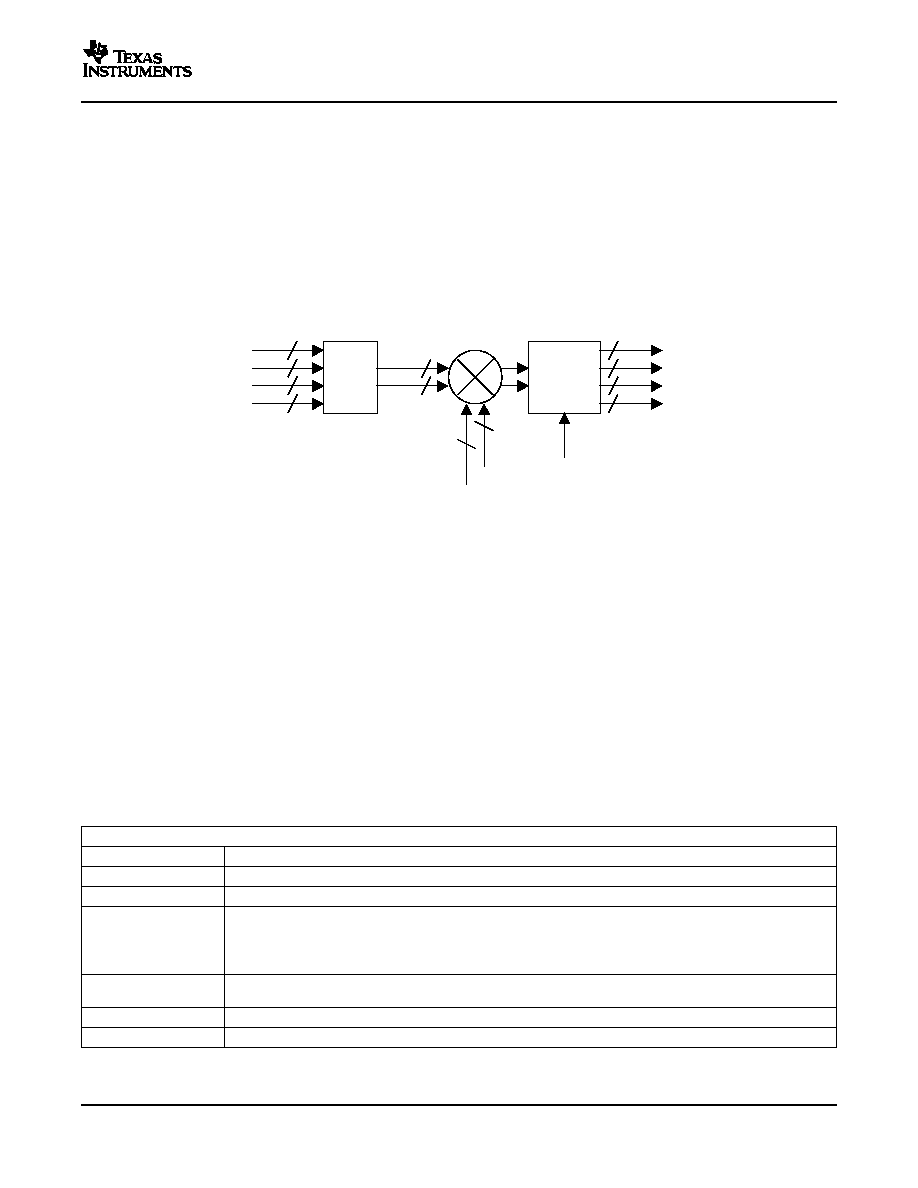
Each GC5018 downconversion block can process two CDMA carriers or a single UMTS carrier. Signal
data is selected from one of four ports for real inputs, or two of four ports for complex inputs. Data from
the selected port(s) is multiplied with a complex, programmable numerically controlled oscillator (NCO)
16
RECEIVE DIGITAL SIGNAL PROCESSING
www.ti.com
PRODUCT PREVIEW
3.2.2
DDC Mixer
4 to 2
Select
18
18
18
18
Demux
and
Round
from
rx_distribution
bus
18
18
20
20
sin
cos
from NCO
18
18
18
18
I
A
I
B
Q
A
Q
B
to
channel
delay
mixer_gain
GC5018
8-CHANNEL WIDEBAND RECEIVER
SLWS169 ≠ MAY 2005
which tunes the signal of interest to baseband. The delay adjust and zero pad blocks permits adjustment
of the delay in the end-to-end channel. Zero padding interpolates the signal to the rxclk rate. Filtering
consists of a six stage CIC filter which decimates the tuned data by a factor from 4 to 32, a compensating
FIR filter (CFIR) which decimates by a factor of two, followed by a programmable FIR filter (PFIR) which
does not decimate. The output interface block can be programmed to decimate by 2 if desired.
The RMS power meter measures the power within the channel's bandwidth. The AGC automatically drives
the gain and keeps the magnitude of the signal at a user-specified level. This allows fewer bits to
represent the signal. The serial output interface formats and rounds the output data. Each of the above
blocks is described in greater detail in the following sections.
The receive mixer translates the input (from one of the input signal sources) to baseband where
subsequent filtering is performed to isolate the signal of interest. The mixer is a complex multiplier that
accepts 18 bit I and 18 bit Q signal data from the receive input interface and 20 bit Sine and Cosine
sequences from the NCO. The NCO generates a mixing frequency (sometimes referred to as a local
oscillator, or LO) specified by the user so that the desired signal of interest is tuned to 0 Hertz.
A DDC channel can support one UMTS signal directly, or two CDMA channels at half the input rate. When
in CDMA mode each channel may set independently; the path selection and the mixer tuning and phase.
The mixer output produces two complex streams; one representing the signal path for the A-side DDC, the
other the B-side. Each of these streams drives a channel delay and zero pad block.
The maximum input rate for UMTS is rxclk for either real or complex input data.
The maximum input rate in CDMA mode with real inputs is rxclk (remix_only is set, see below).
The maximum input rate in CDMA mode with complex inputs is rxclk/2 due to sharing of multiplier
resources.
PROGRAMMING
VARIABLE
DESCRIPTION
ddcmux_sel_a(3:0)
Programs the I and Q complex input data routing onto two of the four input ports for stream A of CDMA DDC
ddcmux_sel_b(3:0)
Programs the I and Q complex input data routing onto two of the four input ports for stream B of CDMA DDC
remix_only
For CDMA mode only, set this bit for real input data at the rxclk rate.
For complex inputs in CDMA mode, the maximum input data rate is rxclk/2, and this bit must be cleared.
For CDMA mode with real inputs at the rxclk/2 rate or lower, this bit must be cleared
zero_qsample
When set, the Q samples used by the mixer are always zero. This bit should be set for real only inputs in UMTS
mode, or real only inputs in CDMA mode when the input sample rate is rxclk/2 or lower.
ch_rate_sel(1:0)
Specifies the input channel data rate (rxclk, rxclk/2, rxclk/4, or rxclk/8 MSPS).
mixer_gain
When asserted, adds 6dB of gain in the mixer. This gain is highly recommended.
RECEIVE DIGITAL SIGNAL PROCESSING
17

www.ti.com
PRODUCT PREVIEW
3.2.3
DDC Number Controlled Oscillator (NCO)
Reg
32
Frequency Word
32
Frequency Sync
Reg
32
Zero Phase Sync
Clear
23
Reg
16
Phase Offset
16
Phase Offset Sync
Aligned
to top
32 bits
23
sin/cos
table
20
20
Dither
Generator
Dither Sync
5
Aligned
to bottom
5 bits
cos
sin
a) Worst Case Spectrum Without Dither
b) Spectrum With Dither (Tuned to Same Frequency
GC5018
8-CHANNEL WIDEBAND RECEIVER
SLWS169 ≠ MAY 2005
The NCO is a digital complex oscillator that is used to translate (or downconvert) an input signal of interest
to baseband. The block produces programmable complex digital sinusoids by accumulating a frequency
word which is programmed by the user. The output of the accumulator is a phase argument that indexes
into a sin/cos ROM table which produces the complex sinusoid. A phase offset can be added prior to
indexing if desired for channel calibration purposes. This will change the sin/cos phase with respect to
other channels' NCOs.
A 5-bit dither generator is provided and generates a small level of digital pseudo-noise that is added to the
phase argument below the bottom bits and is useful for reducing NCO spurious outputs. This dither
generation is enabled by setting the dither_ena bit; the magnitude of the dither can be reduced by setting
one or both of the dither_mask bits
DITHER PROGRAMMING
VARIABLE
DESCRIPTION
dither_ena
When set turns dither on. Clearing turns dither off.
dither_mask(1:0)
Masks the MSB and MSB-1 dither bits, respectively, when set.
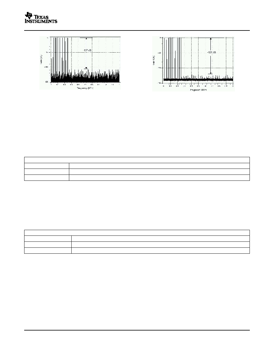
The NCO spurious levels are better than ≠115 dBC. Added phase dither randomizes the periodic nature of
the phase accumulation process and reduces low-level spurious energy. For some frequencies (KxFs/24)
dither is ineffective ≠ in these cases an initial phase of 4 reduces NCO spurs. The figures below show the
spur level performance of the NCO without dither, with dither, and with a phase offset value.
18
RECEIVE DIGITAL SIGNAL PROCESSING
www.ti.com
PRODUCT PREVIEW
a) Plot Without Dither or Phase Initialization
b) Plot With Dither or Phase Initialization
GC5018
8-CHANNEL WIDEBAND RECEIVER
SLWS169 ≠ MAY 2005
The tuning frequency is specified as a 32 bit Frequency Word and is programmed as two sequential 16 bit
words over the control port. The NCO frequency resolution is Fclk/ 232. As an example, at an input clock
rate of 61.44 MHz, the frequency step size would be approximately 14 milli-Hertz. The Frequency Word is
determined by the formula:
Frequency Word (in decimal)= 2
32
x Tuning Frequency / F
clk
Note that frequency tuning words can be positive or negative valued. Specifying a positive frequency
value translates complex negative frequencies upwards towards 0 Hertz. Specifying a negative tuning
frequency translates complex positive frequencies downwards towards 0 Hertz.
FREQUENCY PROGRAMMING
VARIABLE
DESCRIPTION
phase_add_a(31:0)
32 bit tuning frequency word for the A-side DDC when in CDMA mode. Also for UMTS mode.
phase_add_b(31:0)
32 bit tuning frequency word for the B-side DDC when in CDMA mode. Not used in UMTS mode.
Each of the 16 CDMA DDC channels can be loaded with unique frequency words.
The phase of the NCO's Sin/Cos output can be adjusted relative to the phase of other channel NCOs by
specifying a Phase Offset. The Phase Offset is programmed as a 16 bit word, yielding a step size of about
5.5 m∞. The Phase Offset Word is determined by the formula:
Phase Offset Word = 2
16
x Offset_in_Degrees / 360 or,
Phase Offset Word = 2
16
x Offset_in_Radians / 2
PHASE PROGRAMMING
VARIABLE
DESCRIPTION
phase_offset_a(15:0)
16 bit phase offset word for the A-side DDC when in CDMA mode. Also for UMTS mode.
phase_offset_b(15:0)
16 bit phase offset word for the B-side DDC when in CDMA mode. Not used in UMTS mode.
Each of the 16 CDMA DDC channels can be loaded with unique phase offset words.
Various synchronization signals are available which are used to synchronize the NCOs of all channels
with respect to each other. Frequency Sync and Phase Offset Sync determine when frequency and phase
offset changes occur. For example, generating a Frequency Sync after programming the two frequency
words will cause the NCO (or multiple NCOs) to change frequency at that time, rather than after each of
the three frequency words is programmed over the control bus. The Zero Phase Sync signal is used to
force the sine and cosine oscillators to their zero phase state. Dither Sync can be used to synchronize the
dither generators of multiple NCOs. The NCOs used in the transmit section are identical to what is
described for the receive section. Note that there is one set of sync's provided for each DDC. When one
DDC is used to process two CDMA signals, the syncs are shared between them.
RECEIVE DIGITAL SIGNAL PROCESSING
19
www.ti.com
PRODUCT PREVIEW
3.2.4
DDC Filtering and Decimation
Delay
Adjust
Zero Pad
Interp by {1,2,4,8}
Six Stage
CIC Filter
Dec by {4 -32}
CFIR Filter
Dec by 2
PFIR Filter
no decimation
Output Interface
Dec by {1,2}
Delay
Adjust
Zero Pad
Interp by {1,2,4,8}
Six Stage
CIC Filter
Dec by {4 -32}
CFIR Filter
Dec by 2
PFIR Filter
no decimation
From
Mixer
GC5018
8-CHANNEL WIDEBAND RECEIVER
SLWS169 ≠ MAY 2005
SYNC PROGRAMMING
VARIABLE
DESCRIPTION
ssel_nco(2:0)
Sync source for NCO accumulator reset
ssel_dither(2:0)
Sync source for NCO dither reset
ssel_freq(2:0)
Sync source for NCO frequency register loading
ssel_phase(2:0)
Sync source for NCO phase register loading
The purpose of the receive filter chain is to isolate the signal of interest (and reject all other others) that
has been previously translated to baseband via the mixer and NCO. The overall decimation through the
chain needs to be considered. The goal, generally, is to output the isolated signal at a rate that is twice
(2X) the signal's chip rate. For UMTS this would be 7.68 MSPS and for CDMA the output rate should be
2.4576 MSPS. TD-SCDMA systems require the output rate be the chip rate of 1.28 MSPS. The output
interface is programmed to decimate by 2 for the TD-SCDMA case.
Receive filtering and decimation is performed in several stages:
∑
Zero padding to interpolate the input sample rate (if needed) up to the rxclk rate
∑
High rate decimation (4 to 32) using a six stage cascade-integrate-comb filter (CIC)
∑
Decimate by two compensation filtering using the programmable compensating FIR filter (CFIR)
∑
Pulse-shape filtering via the programmable FIR filter (PFIR) with no decimation
∑
Output interface, serial or parallel format, with no decimation or decimate by 2
The table below contains some examples of decimation and sample rates at the output of each block for
UMTS, CDMA and TD-SCDMA standards at various supported input samples. For each example, the
differential ADC clocks are provided to the GC5018 at the input sample rate and the rxclk is provided at
the zero pad output rate.
20
RECEIVE DIGITAL SIGNAL PROCESSING

www.ti.com
PRODUCT PREVIEW
3.2.5
DDC Channel Delay Adjust and Zero Insertion
18
input rate
samples from
Mixer
read offset
3
insert offset
sync (zero stuff moment)
Zero
Pad
18
I
Q
Delay Memory
I:8 slots x 18-bits
Q:8 slots x 18-bits
18
18
18
18
I
Q
3
full rxclk rate
samples to
CIC Filter
sync (offset registers)
interpolation
(number of zeros stuffed between samples)
3
GC5018
8-CHANNEL WIDEBAND RECEIVER
SLWS169 ≠ MAY 2005
Table 3-1. Examples of Decimation and Sample Rates
(1)
Input
Zeros
rxclk(MHz) and
CIC
CIC Out-
CFIR
CFIR
PFIR
PFIR Out-
Output
Sample
Added
Zero Pad
Decimation
put Rate
Decimation
Output
Decimation
put Rate
Decimation
Rate
Output Rate
(MSPS)
Rate
(MSPS)
(MSPS)
(MSPS)
(MSPS)
UMTS
122.88
0
122.88
8
15.36
2
7.68
1
7.68
1
UMTS
92.16
0
92.16
6
15.36
2
7.68
1
7.68
1
UMTS
76.80
1
153.6
10
15.36
2
7.68
1
7.68
1
UMTS
61.44
1
122.88
8
15.36
2
7.68
1
7.68
1
CDMA
122.88
0
122.88
25
4.9152
2
2.4576
1
2.4576
1
CDMA
78.6432
0
78.6432
16
4.9152
2
2.4576
1
2.4576
1
CDMA
78.6432
1
157.2864
32
4.9152
2
2.4576
1
2.4576
1
CDMA
61.44
1
122.88
25
4.9152
2
2.4576
1
2.4576
1
TD-SCDMA
92.16
0
92.16
18
5.12
2
2.56
1
2.56
2
TD-SCDMA
81.92
0
81.92
16
5.12
2
2.56
1
2.56
2
TD-SCDMA
76.80
0
76.80
15
5.12
2
2.56
1
2.56
2
TD-SCDMA
76.80
1
153.6
30
5.12
2
2.56
1
2.56
2
TD-SCDMA
1
122.88
24
5.12
2
2.56
1
2.56
2
(1)
The DDC output interfaces, both serial and parallel formats, can be programmed to decimate by 2. For the TD-SCDMA examples listed
above, the DDC output rate is 1.28Msps (1x chip rate).
The Receive Channel Delay Adjust function is used to add programmable delays in the channel
downconvert path. Adjusting channel delay can be used to compensate for analog elements external to
the GC5018 digital downconversion such as cables, splitters, analog downconverters, filters, etc.
The Delay Memory block consists of an 8 register memory and a state machine. The state machine uses
a counter to control the write (input) pointer, and the programmed read offset register data to create a
read (output) pointer. Programming larger read offset register values increases the effective delay at a
resolution equal to the input sample rate.
The Zero Pad block is used in conjunction with the Delay Memory for delay adjustments. For example,
with input rates of rxclk/8, the Zero Pad block interpolates the input data to rxclk by inserting 7 zeros. The
Zero Pad's sync insert offset 3-bit control specifies when the zeros are inserted relative to the Sync signal.
This permits a fine adjustment at the rxclk resolution.
RECEIVE DIGITAL SIGNAL PROCESSING
21
www.ti.com
PRODUCT PREVIEW
3.2.6
DDC CIC Filter
Z
-
1
Z
-
1
Z
-
1
Z
-
1
Z
-
1
Z
-
m1
Z
-
1
Z
-
m 2
Z
-
m 3
Z
-
m 4
Z
-
m 5
Z
-
m 6
Shift
m1, m2, m3, m4, m5, m6 = 1 or 2
Decimate
by 4-32
N
Round
&
L imit
24
18
Sh ift
0-3 1
18
54
24
GC5018
8-CHANNEL WIDEBAND RECEIVER
SLWS169 ≠ MAY 2005
The read offset register, tadf_offset_course_a/b, and the insert offset register, tadj_offset_fine_a/b, are
double buffered. Writes to these registers may occur anytime, but the actual values used by the circuit will
not be updated until a register sync
PROGRAMMING
VARIABLE
DESCRIPTION
tadj_offset_coarse_a(2:0)
Read offset into the 8 element memory for the UMTS or CDMA mode A channel DDC.
tadj_offset_coarse_b(2:0)
Read offset into the 8 element memory for the CDMA mode B channel DDC when in CDMA mode.
tadj_offset_fine_a(2:0)
Controls the zero pad (or stuff) insert offset (fine adjust) for the UMTS or CDMA mode A channel of the
DDC.
tadj_offset_fine_b(2:0)
Controls the zero pad (or stuff) insert offset (fine adjust) for the CDMA mode B channel of the DDC
when in CDMA mode.
tadj_interp(2:0)
The interpolation value (1, 2, 4, or 8). Same used for both the A and B channels when in CDMA mode.
Selects the number of zeros to be inserted.
ssel_tadj_fine(2:0)
Selects the sync source for the fine time adjust zero stuff moment. Same for A and B channels when in
CDMA mode.
ssel_tadj_reg(2:0)
Selects the sync source used to update the double buffer course and fine delay selection registers.
Same for A and B channels when in CDMA mode.
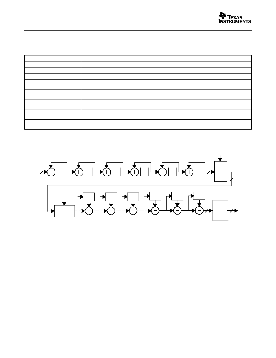
The CIC filter provides the first stage of filtering and large-value decimation. The filter consists of six
stages and decimates over a range from 4 to 32.
I data and Q data are handled separately with two CIC filters. In addition, when in CDMA mode (two
CDMA channels processed within a single DDC), another pair of CIC filters handles the B-side channel.
The filter response is 6x(Sin(x)/x) in character where the key attribute is that the resulting response nulls
reject signal aliases from decimation. A consequence of this desirable behavior is that only a small portion
of the passband can be used, less than 25% generally. This means that the CIC decimation value should
be chosen so that the signal exiting the CIC filter is oversampled by at least a factor of four.
The filter is equivalent to 6 stages of a FIR filter with uniform coefficients (6 combined boxcar filter stages).
Each filter would be of length N if m=1, or 2N if m=2.
The filter is made up of six banks of 54 bit accumulator sections followed by six banks of 24 bit subtractor
sections. Each of the subtractor sections can be independently programmed with a differential delay of
either one or two. A shift block follows the last integration stage and can shift the 54 bit accumulated data
down by 36-rcic_shift (a programmable factor from 0 to 31 bits).
22
RECEIVE DIGITAL SIGNAL PROCESSING

www.ti.com
PRODUCT PREVIEW
3.2.7
DDC Compensating FIR Filter (CFIR)
GC5018
8-CHANNEL WIDEBAND RECEIVER
SLWS169 ≠ MAY 2005
The CIC filter exhibits a droop across its frequency response. The following CFIR filter compensates for
the CIC droop with a gradually rising frequency response. It is also possible to compensate for CIC droop
in the PFIR filter.
The gain of the receive CIC filter is:
Ncic
6
x 2
(number of stages where M=2)
x 2
(≠36+RCIC_SHIFT)
where RCIC_SHIFT is 0 to 31.
There is no rollover protection internal to the CIC or at the final round so the user must guarantee no
sample exceeds full scale prior to rounding. For practical purposes this means the CIC gain can only
compensate for peak gain less than one or must be less than or equal to one. A fixed gain of +12 dB at
the output of the CIC can also be programmed.
PROGRAMMING
VARIABLE
DESCRIPTION
cic_decim(4:0)
The CIC decimation ratio (4 to 32). The ratio is cic_decim + 1. This ratio applies to both A and B channels of
the DDC block in CDMA mode.
cic_scale_a(4:0)
The shift value for the A channel. A value of 0 is no shift, each increment in value increases the amplitude of
the shifter output by a factor of 2.
cic_scale_b(4:0)
The shift value for the B channel. A value of 0 is no shift, each increment in value increases the amplitude of
the shifter output by a factor of 2.
cic_gain_ddc
When asserted, adds a gain of 12 dB at the CIC output.
cic_m2_ena_a(5:0)
Sets the differential delay value M for each of the CIC subtractor stages for the UMTS or CDMA mode A
channel.
cic_m2_ena_b (5:0)
Sets the differential delay value M for each of the CIC subtractor stages for the CDMA mode B channel.
cic_bypass
Bypasses the CIC filter when set, for factory testing.
ssel_cic(2:0)
Sets syncing (1 of 8 sources) for the CIC decimation moment.
The receive compensating FIR filter (CFIR) decimates the output of the CIC filter by a fixed factor of two.
Filter coefficient size, input data size, and output data size are 18 bits. The CFIR length can be
programmed. This permits "turning off" taps and saving power if shorter filters are appropriate (the CFIR
power dissipation is proportional to its length).
The filter is organized in two partial filter blocks, each containing a data RAM, a coefficient RAM and a
dual multiplier, a common state machine and output accumulator.
RECEIVE DIGITAL SIGNAL PROCESSING
23

www.ti.com
PRODUCT PREVIEW
MPU control
interface
complex
input
samples
COEF
RAM
32x18
DATA
RAM
64x36
reg
complex
output
samples
crastarttap
State Machine
output
sample
valid
read
pointer
write
pointer
write pointer
MUX
read pointer
mpu
ram_read
read data
write data
COEF
RAM
32x18
DATA
RAM
64x36
GC5018
8-CHANNEL WIDEBAND RECEIVER
SLWS169 ≠ MAY 2005
The maximum CFIR filter length is a function of GC5018 clock rate, output sample rate and the number of
coefficient memory registers. The maximum number of taps is 64 and the minimum number is 14. Lengths
between these limits can be specified in increments of 2.
Subject to the above minimum and maximum values, in the general case, the number of taps available is:
UMTS Mode: 2 x (rxclk ˜ output sample rate)
CDMA Mode if cic_decim is even (decimating by an odd number): 2 x (cic_decim)
CDMA Mode if cic_decim is odd (decimating by an even number): 2 x (cic_decim + 1)
Example CFIR filter lengths available based on mode and rxclk frequency:
Mode
rxclk
CIC
CFIR
CFIR
COMMENTS
(MHz)
DECIMATION
MAX LENGTH
MIN LENGTH
UMTS
153.60
10
40
14
UMTS
UMTS
122.88
8
32
14
UMTS
CDMA
157.2864
32
64
14
CDMA2000
CDMA
122.88
25
48
14
CDMA2000
CDMA
78.6432
16
32
14
CDMA2000 low power configuration
CDMA
153.60
30
60
14
TD-SCDMA
CDMA
81.92
16
32
14
TD-SCDMA
CDMA
76.80
15
28
14
TD-SCDMA low power configuration
24
RECEIVE DIGITAL SIGNAL PROCESSING

www.ti.com
PRODUCT PREVIEW
GC5018
8-CHANNEL WIDEBAND RECEIVER
SLWS169 ≠ MAY 2005
A single set of programmed tap values are used for both the A-side and B-side DDC channels (two CDMA
channels) within a single DDC block when in CDMA mode.
After the CFIR filter performs the convolution, gain is applied at full precision, the signal is rounded, and
then hard limited. A shifter at the output of the filter then scales the data by either 2e-19 or 2e-18. The
gain through the filter is therefore:
Sum(CFIR coefficients) x 2
≠(18 or 19)
Coefficients are organized in two groups of 32 words, each 18 bits wide. For fully utilized filters, the 64
coefficients are loaded 0 through 31 into the first RAM, and 32 through 63 into the second RAM. The 16
bit MSBs and 2 bit LSBs are written into the RAMs using different page register values. Shorter filters
require the coefficients be loaded into the 2 rams equally, starting from address 0.
For example, a CFIR coefficient set for a symmetric 58 tap TD-SCDMA CFIR is:
Taps
Coefficient
Taps
Coefficient
0 = 57
≠13
15 = 42
≠4975
1 = 56
≠20
16 = 41
≠4649
2 = 55
14
17 = 40
≠232
3 = 54
101
18 = 39
6581
4 = 53
184
19 = 38
11266
5 = 52
133
20 = 37
8917
6 = 51
≠147
21 = 36
≠1957
7 = 50
≠562
22 = 35
≠16736
8 = 49
≠768
23 = 34
≠25469
9 = 48
≠364
24 = 33
≠ 17599
10 = 47
719
25 = 32
11560
11 = 46
1905
26 = 31
56455
12 = 45
2126
27 = 30
102215
13 = 44
567
28 = 29
131071
14 = 43
≠2416
The first 29 coefficients are loaded into addresses 0 through 28 in the first coefficient RAM, and the
remaining 29 are loaded into addresses 0 through 28 in the second coefficient RAM. Loading the 18 bit
coefficients requires 2 writes per coefficient, one for the upper 16 bits and another for the lower 2 bits.
To program this coefficient set for the DDC2 CFIR, the following control microprocessor interface
sequence would be used.
Step
Address
Data
Description
a[5:0]
d[15:0]
1
0x21
0x0480
Page register for DDC2 CFIR Coefficient RAM 0-31, LSBs.
2
0x00
0x0003
2 lower bits of coefficient 0
3
0x01
0x0000
2 lower bits of coefficient 1
4
0x02
0x0002
2 lower bits of coefficient 2
5
0x03
0x0001
2 lower bits of coefficient 3
6
0x04
0x0000
2 lower bits of coefficient 4
7
0x05
0x0001
2 lower bits of coefficient 5
8
0x06
0x0001
2 lower bits of coefficient 6
9
0x07
0x0002
2 lower bits of coefficient 7
10
0x08
0x0000
2 lower bits of coefficient 8
11
0x09
0x0000
2 lower bits of coefficient 9
12
0x0A
0x0003
2 lower bits of coefficient 10
RECEIVE DIGITAL SIGNAL PROCESSING
25

www.ti.com
PRODUCT PREVIEW
GC5018
8-CHANNEL WIDEBAND RECEIVER
SLWS169 ≠ MAY 2005
Step
Address
Data
Description
a[5:0]
d[15:0]
13
0x0B
0x0001
2 lower bits of coefficient 11
14
0x0C
0x0002
2 lower bits of coefficient 12
15
0x0D
0x0003
2 lower bits of coefficient 13
16
0x0E
0x0000
2 lower bits of coefficient 14
17
0x0F
0x0001
2 lower bits of coefficient 15
18
0x10
0x0003
2 lower bits of coefficient 16
19
0x11
0x0000
2 lower bits of coefficient 17
20
0x12
0x0001
2 lower bits of coefficient 18
21
0x13
0x0002
2 lower bits of coefficient 19
22
0x14
0x0001
2 lower bits of coefficient 20
23
0x15
0x0003
2 lower bits of coefficient 21
24
0x16
0x0000
2 lower bits of coefficient 22
25
0x17
0x0003
2 lower bits of coefficient 23
26
0x18
0x0001
2 lower bits of coefficient 24
27
0x19
0x0000
2 lower bits of coefficient 25
28
0x1A
0x0003
2 lower bits of coefficient 26
29
0x1B
0x0003
2 lower bits of coefficient 27
30
0x1C
0x0003
2 lower bits of coefficient 28
31
0x1D
0x0000
2 lower bits of unused coefficient RAM location
32
0x1E
0x0000
2 lower bits of unused coefficient RAM location
33
0x1F
0x0000
2 lower bits of unused coefficient RAM location
34
0x21
0x04A0
Page register for DDC2 CFIR Coefficient RAM 32-63, LSBs.
35
0x00
0x0003
2 lower bits of coefficient 29
36
0x01
0x0003
2 lower bits of coefficient 30
37
0x02
0x0003
2 lower bits of coefficient 31
38
0x03
0x0000
2 lower bits of coefficient 32
39
0x04
0x0001
2 lower bits of coefficient 33
40
0x05
0x0003
2 lower bits of coefficient 34
41
0x06
0x0000
2 lower bits of coefficient 35
42
0x07
0x0003
2 lower bits of coefficient 36
43
0x08
0x0001
2 lower bits of coefficient 37
44
0x09
0x0002
2 lower bits of coefficient 38
45
0x0A
0x0001
2 lower bits of coefficient 39
46
0x0B
0x0000
2 lower bits of coefficient 40
47
0x0C
0x0003
2 lower bits of coefficient 41
48
0x0D
0x0001
2 lower bits of coefficient 42
49
0x0E
0x0000
2 lower bits of coefficient 43
50
0x0F
0x0003
2 lower bits of coefficient 44
51
0x10
0x0002
2 lower bits of coefficient 45
52
0x11
0x0001
2 lower bits of coefficient 46
53
0x12
0x0003
2 lower bits of coefficient 47
54
0x13
0x0000
2 lower bits of coefficient 48
55
0x14
0x0000
2 lower bits of coefficient 49
56
0x15
0x0002
2 lower bits of coefficient 50
57
0x16
0x0001
2 lower bits of coefficient 51
58
0x17
0x0001
2 lower bits of coefficient 52
59
0x18
0x0000
2 lower bits of coefficient 53
60
0x19
0x0001
2 lower bits of coefficient 54
26
RECEIVE DIGITAL SIGNAL PROCESSING

www.ti.com
PRODUCT PREVIEW
GC5018
8-CHANNEL WIDEBAND RECEIVER
SLWS169 ≠ MAY 2005
Step
Address
Data
Description
a[5:0]
d[15:0]
61
0x1A
0x0002
2 lower bits of coefficient 55
62
0x1B
0x0000
2 lower bits of coefficient 56
63
0x1C
0x0003
2 lower bits of coefficient 57
64
0x1D
0x0000
2 lower bits of unused coefficient RAM location
65
0x1E
0x0000
2 lower bits of unused coefficient RAM location
66
0x1F
0x0000
2 lower bits of unused coefficient RAM location
67
0x21
0x04C0
Page register for DDC2 CFIR Coefficient RAM 0-31, MSBs.
68
0x00
0xFFFC
Upper 16 bits of coefficient 0
69
0x01
0xFFFB
Upper 16 bits of coefficient 1
70
0x02
0x0003
Upper 16 bits of coefficient 2
71
0x03
0x0019
Upper 16 bits of coefficient 3
72
0x04
0x002E
Upper 16 bits of coefficient 4
73
0x05
0x0021
Upper 16 bits of coefficient 5
74
0x06
0xFFDB
Upper 16 bits of coefficient 6
75
0x07
0xFF73
Upper 16 bits of coefficient 7
76
0x08
0xFF40
Upper 16 bits of coefficient 8
77
0x09
0xFFA5
Upper 16 bits of coefficient 9
78
0x0A
0x00B3
Upper 16 bits of coefficient 10
79
0x0B
0x01DC
Upper 16 bits of coefficient 11
80
0x0C
0x0213
Upper 16 bits of coefficient 12
81
0x0D
0x008D
Upper 16 bits of coefficient 13
82
0x0E
0xFDA4
Upper 16 bits of coefficient 14
83
0x0F
0xFB24
Upper 16 bits of coefficient 15
84
0x10
0xFB75
Upper 16 bits of coefficient 16
85
0x11
0xFFC6
Upper 16 bits of coefficient 17
86
0x12
0x066D
Upper 16 bits of coefficient 18
87
0x13
0x0B00
Upper 16 bits of coefficient 19
88
0x14
0x08B5
Upper 16 bits of coefficient 20
89
0x15
0xFE16
Upper 16 bits of coefficient 21
90
0x16
0xEFA8
Upper 16 bits of coefficient 22
91
0x17
0xE720
Upper 16 bits of coefficient 23
92
0x18
0xEED0
Upper 16 bits of coefficient 24
93
0x19
0x0B4A
Upper 16 bits of coefficient 25
94
0x1A
0x3721
Upper 16 bits of coefficient 26
95
0x1B
0x63D1
Upper 16 bits of coefficient 27
96
0x1C
0x7FFF
Upper 16 bits of coefficient 28
97
0x1D
0x0000
Upper 16 bits of unused coefficient RAM location
98
0x1E
0x0000
Upper 16 bits of unused coefficient RAM location
99
0x1F
0x0000
Upper 16 bits of unused coefficient RAM location
100
0x21
0x04E0
Page register for DDC2 CFIR Coefficient RAM 32-63, MSBs.
101
0x00
0x7FFF
Upper 16 bits of coefficient 29
102
0x01
0x63D1
Upper 16 bits of coefficient 30
103
0x02
0x3721
Upper 16 bits of coefficient 31
104
0x03
0x0B4A
Upper 16 bits of coefficient 32
105
0x04
0xEED0
Upper 16 bits of coefficient 33
106
0x05
0xE720
Upper 16 bits of coefficient 34
107
0x06
0xEFA8
Upper 16 bits of coefficient 35
108
0x07
0xFE16
Upper 16 bits of coefficient 36
RECEIVE DIGITAL SIGNAL PROCESSING
27

www.ti.com
PRODUCT PREVIEW
3.2.8
DDC Programmable FIR Filter (PFIR)
GC5018
8-CHANNEL WIDEBAND RECEIVER
SLWS169 ≠ MAY 2005
Step
Address
Data
Description
a[5:0]
d[15:0]
109
0x08
0x08B5
Upper 16 bits of coefficient 37
110
0x09
0x0B00
Upper 16 bits of coefficient 38
111
0x0A
0x066D
Upper 16 bits of coefficient 39
112
0x0B
0xFFC6
Upper 16 bits of coefficient 40
113
0x0C
0xFB75
Upper 16 bits of coefficient 41
114
0x0D
0xFB24
Upper 16 bits of coefficient 42
115
0x0E
0xFDA4
Upper 16 bits of coefficient 43
116
0x0F
0x008D
Upper 16 bits of coefficient 44
117
0x10
0x0213
Upper 16 bits of coefficient 45
118
0x11
0x01DC
Upper 16 bits of coefficient 46
119
0x12
0x00B3
Upper 16 bits of coefficient 47
120
0x13
0xFFA5
Upper 16 bits of coefficient 48
121
0x14
0xFF40
Upper 16 bits of coefficient 49
122
0x15
0xFF73
Upper 16 bits of coefficient 50
123
0x16
0xFFDB
Upper 16 bits of coefficient 51
124
0x17
0x0021
Upper 16 bits of coefficient 52
125
0x18
0x002E
Upper 16 bits of coefficient 53
126
0x19
0x0019
Upper 16 bits of coefficient 54
127
0x1A
0x0003
Upper 16 bits of coefficient 55
128
0x1B
0xFFFB
Upper 16 bits of coefficient 56
129
0x1C
0xFFFC
Upper 16 bits of coefficient 57
130
0x1D
0x0000
Upper 16 bits of unused coefficient RAM location
131
0x1E
0x0000
Upper 16 bits of unused coefficient RAM location
132
0x1F
0x0000
Upper 16 bits of unused coefficient RAM location
133
0x21
0x0500
Page register for DDC2 control registers 0-31
134
0x00
0x8EE0
DDC2 FIR_MODE register; cdma_mode enabled, 60 tap PFIR, 58 tap CFIR
135
0x01
0x2000
DDC2 PFIR gain = sum(taps)x2^≠18 and CFIR gain = sum(taps)x2^≠19
PROGRAMMING
VARIABLE
DESCRIPTION
crastarttap_cfir(4:0)
Number of DDC CFIR filter taps is 2x(crastarttap + 1)
mpu_ram_read
What set, the PFIR and CFIR coefficient rams are readable via the MPU control interface. The GC5018 signal
path is not operational when this bit is set, it is intended for debug purposes only.
cfir_gain
0 = 2e
≠19
, 1 = 2e
≠18
The CFIR filter's 18 bit coefficients are loaded in two 32 word memories.
Note: CFIR filter coefficients are shared between A and B channels of a DDC block in CDMA mode.
The receive programmable FIR filter (PFIR) provides final pulse shaping of the baseband signal data. It
does not perform any decimation. Filter coefficient size, input, and output data size is 18 bits. A special
strapped mode can be employed for UMTS where two adjacent DDCs (2k & 2k+1, k=0 to 7) can be
combined to yield a filter with twice the number of coefficients. This means the GC5018 can support 4
UMTS DDC channels with double-length filter coefficients (up to 128 taps).
The filter is organized in four partial filter blocks, each containing a data RAM, a coefficient RAM and a
dual multiplier, a common state machine and output accumulator.
28
RECEIVE DIGITAL SIGNAL PROCESSING

www.ti.com
PRODUCT PREVIEW
reg
complex
output
samples
output
sample
valid
read
pointer
write
pointer
read pointer
to adjacent DDC
(if double_tap=" 10" )
MPU control
interface
complex input
samples from cfir
(or adjacent DDC if
double_tap="01"
COEF
RAM
16x18
DATA
RAM
32x36
complex
output
samples
crastarttap
State Machine
output
sample
valid
write pointer
MUX
mpu
ram_read
read data
write data
to adjacent DDC
(if double_tap=" 10" )
from adjacent DDC
(if double_tap="10")
Filter cell 1
cell 2
cell 3
cell 4
GC5018
8-CHANNEL WIDEBAND RECEIVER
SLWS169 ≠ MAY 2005
The PFIR length is programmable. This permits turning off taps and saving power if short filters are
appropriate. The filter's output data can be shifted over a range of 0 to 7 bits where it is then rounded and
hard limited to 18 bits. The shift range results in a gain that ranges from 2e
≠19
to 2e
≠12
.
The gain of the PFIR block is: sum(coefficients) x 2-shift, where shift ranges from 12 to 19.
The maximum PFIR filter length is a function of GC5018 clock rate and output sample rate and is limited
by the number of coefficient memory registers. The maximum number of taps is 64 and the minimum
number is 32 (for both CDMA and UMTS). Lengths between these limits can be specified in increments of
4. For strapped UMTS with double length filters, the range of taps available is 64 to 128 in increments of
8.
Subject to the above minimum and maximum values, the number of maximum taps available is:
UMTS Mode: 4 x (rxclk ˜ output sample rate)
Strapped UMTS Mode: 8 x (rxclk ˜ output sample rate)
CDMA Mode: 2 x (rxclk ˜ output sample rate)
PFIR coefficients and gain shift values are shared between both A and B CDMA channels in a DDC block.
Example PFIR filter lengths available based on mode and rxclk frequency:
Mode
rxclk
CIC
PFIR
PFIR
COMMENTS
(MHz)
DECI-
MAX LENGTH
MIN LENGTH
MATION
UMTS
153.60
10
64
32
UMTS, 1 to 6 DDC channels
UMTS
122.88
8
64
32
UMTS, 1 to 6 DDC channels
UMTS
153.60
10
128
64
Strapped UMTS double length PFIR configuration; 1, 2 or 3 DDC
channels.
UMTS
122.88
8
128
64
Strapped UMTS double length PFIR configuration; 1, 2 or 3 DDC
channels
RECEIVE DIGITAL SIGNAL PROCESSING
29

www.ti.com
PRODUCT PREVIEW
GC5018
8-CHANNEL WIDEBAND RECEIVER
SLWS169 ≠ MAY 2005
Mode
rxclk
CIC
PFIR
PFIR
COMMENTS
(MHz)
DECI-
MAX LENGTH
MIN LENGTH
MATION
CDMA
157.2864
32
64
32
CDMA2000
CDMA
122.88
25
64
32
CDMA2000
CDMA
78.6432
16
64
32
CDMA2000 low power configuration
CDMA
153.60
30
64
32
TD-SCDMA
CDMA
81.92
16
64
32
TD-SCDMA
CDMA
76.80
15
60
32
TD-SCDMA low power configuration
Coefficients are organized in four groups of 16 words, each 18 bits wide. For fully utilized filters, the 64
coefficients are loaded 0 through 31 into the first and second RAMs, and 32 through 63 into the third and
fourth RAMs. The 16 bit MSBs and 2 bit LSBs are written into the RAMs using different page register
values. Shorter filters require the coefficients be loaded into the 4 rams equally, starting from address 0
and address 16.
For example, a CFIR coefficient set for a symmetric 60 tap TD-SCDMA PFIR is:
Taps
Coefficient
Taps
Coefficient
0 = 59
≠2
15 = 44
420
1 = 58
1
16 = 43
≠331
2 = 57
4
17 = 42
≠319
3 = 56
≠8
18 = 41
744
4 = 55
≠2
19 = 40
≠440
5 = 54
21
20 = 39
≠1005
6 = 53
≠13
21 = 38
2389
7 = 52
≠28
22 = 37
514
8 = 51
46
23 = 36
≠6182
9 = 50
1
24 = 35
1845
10 = 49
≠85
25 = 34
12959
11 = 48
96
26 = 33
≠8691
12 = 47
82
27 = 32
≠27246
13 = 46
≠266
28 = 31
34166
14 = 45
38
29 = 30
131071
The first 15 coefficients are loaded into addresses 0 through 14 in the first coefficient RAM, the second
group of 15 are loaded into addresses 16 through 30 corresponding to the second coefficient RAM, the
third group of 15 are loaded into the third coefficient ram at addresses 0 through 14, and the fourth group
of 15 are loaded into addresses 16 through 30 in the fourth coefficient RAM. Loading the 18 bit
coefficients requires 2 writes per coefficient, one for the upper 16 bits and another for the lower 2 bits.
To program this coefficient set for the DDC2 PFIR, the following control microprocessor interface
sequence would be used.
Step
Address
Data
Description
a[5:0]
d[15:0]
1
0x21
0x0400
Page register for DDC2 CFIR Coefficient RAMs 0-15 and 16-31, LSBs.
2
0x00
0x0002
2 lower bits of coefficient 0
3
0x01
0x0001
2 lower bits of coefficient 1
4
0x02
0x0000
2 lower bits of coefficient 2
5
0x03
0x0000
2 lower bits of coefficient 3
6
0x04
0x0002
2 lower bits of coefficient 4
30
RECEIVE DIGITAL SIGNAL PROCESSING

www.ti.com
PRODUCT PREVIEW
GC5018
8-CHANNEL WIDEBAND RECEIVER
SLWS169 ≠ MAY 2005
Step
Address
Data
Description
a[5:0]
d[15:0]
7
0x05
0x0001
2 lower bits of coefficient 5
8
0x06
0x0003
2 lower bits of coefficient 6
9
0x07
0x0000
2 lower bits of coefficient 7
10
0x08
0x0002
2 lower bits of coefficient 8
11
0x09
0x0001
2 lower bits of coefficient 9
12
0x0A
0x0003
2 lower bits of coefficient 10
13
0x0B
0x0000
2 lower bits of coefficient 11
14
0x0C
0x0002
2 lower bits of coefficient 12
15
0x0D
0x0002
2 lower bits of coefficient 13
16
0x0E
0x0002
2 lower bits of coefficient 14
17
0x0F
0x0000
2 lower bits of unused coefficient RAM location
18
0x10
0x0000
2 lower bits of coefficient 15
19
0x11
0x0001
2 lower bits of coefficient 16
20
0x12
0x0001
2 lower bits of coefficient 17
21
0x13
0x0000
2 lower bits of coefficient 18
22
0x14
0x0000
2 lower bits of coefficient 19
23
0x15
0x0003
2 lower bits of coefficient 20
24
0x16
0x0001
2 lower bits of coefficient 21
25
0x17
0x0002
2 lower bits of coefficient 22
26
0x18
0x0002
2 lower bits of coefficient 23
27
0x19
0x0001
2 lower bits of coefficient 24
28
0x1A
0x0003
2 lower bits of coefficient 25
29
0x1B
0x0001
2 lower bits of coefficient 26
30
0x1C
0x0002
2 lower bits of coefficient 27
31
0x1D
0x0002
2 lower bits of coefficient 28
32
0x1E
0x0003
2 lower bits of coefficient 29
33
0x1F
0x0000
2 lower bits of unused coefficient RAM location
34
0x21
0x0420
Page register for DDC2 CFIR Coefficient RAMs 32-47 and 48-63, LSBs.
35
0x00
0x0003
2 lower bits of coefficient 30
36
0x01
0x0002
2 lower bits of coefficient 31
37
0x02
0x0002
2 lower bits of coefficient 32
38
0x03
0x0001
2 lower bits of coefficient 33
39
0x04
0x0003
2 lower bits of coefficient 34
40
0x05
0x0001
2 lower bits of coefficient 35
41
0x06
0x0002
2 lower bits of coefficient 36
42
0x07
0x0002
2 lower bits of coefficient 37
43
0x08
0x0001
2 lower bits of coefficient 38
44
0x09
0x0003
2 lower bits of coefficient 39
45
0x0A
0x0000
2 lower bits of coefficient 40
46
0x0B
0x0000
2 lower bits of coefficient 41
47
0x0C
0x0001
2 lower bits of coefficient 42
48
0x0D
0x0001
2 lower bits of coefficient 43
49
0x0E
0x0000
2 lower bits of coefficient 44
50
0x0F
0x0000
2 lower bits of unused coefficient RAM location
51
0x10
0x0002
2 lower bits of coefficient 45
52
0x11
0x0002
2 lower bits of coefficient 46
53
0x12
0x0002
2 lower bits of coefficient 47
54
0x13
0x0000
2 lower bits of coefficient 48
RECEIVE DIGITAL SIGNAL PROCESSING
31

www.ti.com
PRODUCT PREVIEW
GC5018
8-CHANNEL WIDEBAND RECEIVER
SLWS169 ≠ MAY 2005
Step
Address
Data
Description
a[5:0]
d[15:0]
55
0x14
0x0003
2 lower bits of coefficient 49
56
0x15
0x0001
2 lower bits of coefficient 50
57
0x16
0x0002
2 lower bits of coefficient 51
58
0x17
0x0000
2 lower bits of coefficient 52
59
0x18
0x0003
2 lower bits of coefficient 53
60
0x19
0x0001
2 lower bits of coefficient 54
61
0x1A
0x0002
2 lower bits of coefficient 55
62
0x1B
0x0000
2 lower bits of coefficient 56
63
0x1C
0x0000
2 lower bits of coefficient 57
64
0x1D
0x0001
2 lower bits of coefficient 58
65
0x1E
0x0002
2 lower bits of coefficient 59
66
0x1F
0x0000
2 lower bits of unused coefficient RAM location
67
0x21
0x0440
Page register for DDC2 PFIR Coefficient RAMs 0-15 and 16-31, MSBs.
68
0x00
0xFFFF
Upper 16 bits of coefficient 0
69
0x01
0x0000
Upper 16 bits of coefficient 1
70
0x02
0x0001
Upper 16 bits of coefficient 2
71
0x03
0xFFFE
Upper 16 bits of coefficient 3
72
0x04
0xFFFF
Upper 16 bits of coefficient 4
73
0x05
0x0005
Upper 16 bits of coefficient 5
74
0x06
0xFFFC
Upper 16 bits of coefficient 6
75
0x07
0xFFF9
Upper 16 bits of coefficient 7
76
0x08
0x000B
Upper 16 bits of coefficient 8
77
0x09
0x0000
Upper 16 bits of coefficient 9
78
0x0A
0xFFEA
Upper 16 bits of coefficient 10
79
0x0B
0x0018
Upper 16 bits of coefficient 11
80
0x0C
0x0014
Upper 16 bits of coefficient 12
81
0x0D
0xFFBD
Upper 16 bits of coefficient 13
82
0x0E
0x0009
Upper 16 bits of coefficient 14
83
0x0F
0x0000
Upper 16 bits of unused coefficient RAM location
84
0x10
0x0069
Upper 16 bits of coefficient 15
85
0x11
0xFFAD
Upper 16 bits of coefficient 16
86
0x12
0x0FFB0
Upper 16 bits of coefficient 17
87
0x13
0x0B0A
Upper 16 bits of coefficient 18
88
0x14
0xFF92
Upper 16 bits of coefficient 19
89
0x15
0xFF04
Upper 16 bits of coefficient 20
90
0x16
0x0255
Upper 16 bits of coefficient 21
91
0x17
0x0080
Upper 16 bits of coefficient 22
92
0x18
0xF9F6
Upper 16 bits of coefficient 23
93
0x19
0x01CD
Upper 16 bits of coefficient 24
94
0x1A
0x0CA7
Upper 16 bits of coefficient 25
95
0x1B
0xF783
Upper 16 bits of coefficient 26
96
0x1C
0xE564
Upper 16 bits of coefficient 27
97
0x1D
0x215D
Upper 16 bits of coefficient 28
98
0x1E
0x7FFF
Upper 16 bits of coefficient 29
99
0x1F
0x0000
Upper 16 bits of unused coefficient RAM location
100
0x21
0x0460
Page register for DDC2 PFIR Coefficient RAMS 32-47 AND 48-63, MSBs.
101
0x00
0x7FFF
Upper 16 bits of coefficient 30
102
0x01
0x215D
Upper 16 bits of coefficient 31
32
RECEIVE DIGITAL SIGNAL PROCESSING

www.ti.com
PRODUCT PREVIEW
GC5018
8-CHANNEL WIDEBAND RECEIVER
SLWS169 ≠ MAY 2005
Step
Address
Data
Description
a[5:0]
d[15:0]
103
0x02
0xE564
Upper 16 bits of coefficient 32
104
0x03
0xF783
Upper 16 bits of coefficient 33
105
0x04
0x0CA7
Upper 16 bits of coefficient 34
106
0x05
0x01CD
Upper 16 bits of coefficient 35
107
0x06
0xF9F6
Upper 16 bits of coefficient 36
108
0x07
0x0080
Upper 16 bits of coefficient 37
109
0x08
0x0255
Upper 16 bits of coefficient 38
110
0x09
0xFF04
Upper 16 bits of coefficient 39
111
0x0A
0xFF92
Upper 16 bits of coefficient 40
112
0x0B
0x00BA
Upper 16 bits of coefficient 41
113
0x0C
0xFFB0
Upper 16 bits of coefficient 42
114
0x0D
0xFFAD
Upper 16 bits of coefficient 43
115
0x0E
0x0069
Upper 16 bits of coefficient 44
116
0x0F
0x008D
Upper 16 bits of unused coefficient RAM location
117
0x10
0x0009
Upper 16 bits of coefficient 45
118
0x11
0xFFBD
Upper 16 bits of coefficient 46
119
0x12
0x0014
Upper 16 bits of coefficient 47
120
0x13
0x0018
Upper 16 bits of coefficient 48
121
0x14
0xFFEA
Upper 16 bits of coefficient 49
122
0x15
0x0000
Upper 16 bits of coefficient 50
123
0x16
0x000B
Upper 16 bits of coefficient 51
124
0x17
0xFFF9
Upper 16 bits of coefficient 52
125
0x18
0xFFFC
Upper 16 bits of coefficient 53
126
0x19
0x0005
Upper 16 bits of coefficient 54
127
0x1A
0xFFFF
Upper 16 bits of coefficient 55
128
0x1B
0xFFFE
Upper 16 bits of coefficient 56
129
0x1C
0x0001
Upper 16 bits of coefficient 57
130
0x1D
0x0000
Upper 16 bits of coefficient 58
131
0x1E
0xFFFF
Upper 16 bits of coefficient 59
132
0x1F
0x0000
Upper 16 bits of unused coefficient RAM location
133
0x21
0x0500
Page register for DDC2 control registers 0-31
134
0x00
0x8EE0
DDC2 FIR_MODE register; cdma_mode enabled, 60 tap PFIR, 58 tap CFIR
135
0x01
0x2000
DDC2 PFIR gain = sum(taps)x2^≠18 and CFIR gain = sum(taps)x2^≠19
PROGRAMMING
VARIABLE
DESCRIPTION
crastarttap_pfir(4:0)
Number of DDC PFIR filter taps is 4x(crastartap+1)
For double length PFIR the number of taps is 8x(crastartap+1)
cdma_mode
When set, puts the CFIR & PFIR blocks in CDMA mode.
mpu_ram_read
What set, the PFIR and CFIR coefficient rams are readable via the MPU control interface.
The GC5018 signal path is not operational when this bit is set, it is intended for debug purposes only.
pfir_gain(2:0)
Sets the gain of the PFIR filter.
The range is from 2e
≠19
to 2e
≠12
; "000"= 2e
≠19
and "111"= 2e
≠12
double_tap(1:0)
When set, puts two adjacent DDC (2k and 2k+1, k=0 to 2) in double length (from 64 to128 tap) UMTS
mode.
Set to "00" for normal mode.
RECEIVE DIGITAL SIGNAL PROCESSING
33
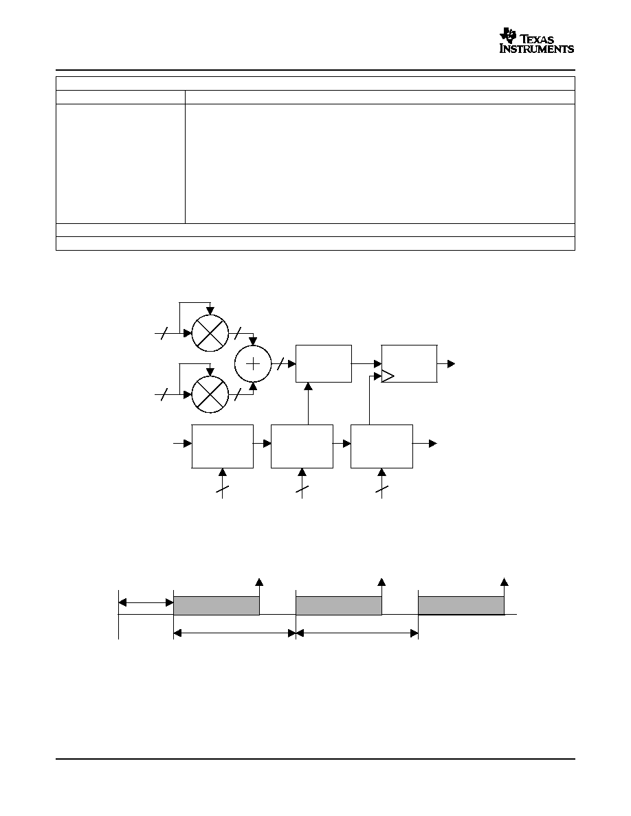
www.ti.com
PRODUCT PREVIEW
3.2.9
DDC RMS Power Meter
55-bit
Integrator
55-bit
Register
8-bit
sync delay
counter
18-bit
interval
counter
18-bit
integration
counter
clear
transfer
interrupt
sync
delay
(in samples)
interval
(in 1024 sample
increments)
integration
(in 4 sample
increments)
16
8
8
RMS power
I
Q
37
36
36
18
18
integration time
integration time
interrupt
interrupt
sync
delay
sync
event
interval time
integration
start
integration
start
integration time
interrupt
interval time
integration
start
GC5018
8-CHANNEL WIDEBAND RECEIVER
SLWS169 ≠ MAY 2005
PROGRAMMING
VARIABLE
DESCRIPTION
In double tap mode, data out of the last PFIR ram in the main DDC (DDC0, DDC2, DDC4 or DDC6) is
sent to the adjacent secondary DDC (DDC1, DDC3, DDC5 or DDC7) PFIR as input thus forming a
128-tap delay line. Data received from the adjacent PFIR summers is added into the Main DDC's PFIR
sum to form the final output.
When using double tap mode, set double_tap to "10" for the main DDC, and to "01" for the secondary
DDC.
When in double tap mode, the first half of the coefficients should be loaded into the main DDC (DDC0,
DDC2, DDC4 or DDC6), the remaining coefficients are loaded into the secondary DDC (DDC1, DDC3,
DDC5 or DDC7).
In double tap mode, the main DDC must be turned on (ddc_ena=1), and the secondary DDC must be
turned off (ddc_ena=0).
The PFIR filter's 18 bit coefficients are loaded in four 16 word memories.
Note: PFIR filter coefficients are shared between A and B channels of a DDC block when in CDMA mode.
Each DDC channel includes an RMS power meter which is used to measure the total power within the
channel pass band.
The power meter samples the I and Q data stream after the PFIR filter. Both 18 bit I and Q data are
squared, summed, and then integrated over a period determined by a programmable counter. The
integration time is a 16 bit word which is programmed into the 18 bit counter.
34
RECEIVE DIGITAL SIGNAL PROCESSING
www.ti.com
PRODUCT PREVIEW
GC5018
8-CHANNEL WIDEBAND RECEIVER
SLWS169 ≠ MAY 2005
There is a programmable 18 bit interval timer which sets the interval over which power measurements are
made. The timer counts in increments of 1024 samples. This allows the user to select intervals from 1 x
1024 samples up to 256 x 1024 samples. For UMTS systems with sample rate rate at 7.68 MHz, the
power meter interval range is from 133 µS to 34.1 mS. For a CDMA system with the sample rate at
2.4576 MHz, the power meter interval range is 417 µS to 107 mS.
The power measurement process starts with a sync event. The integration will start at sync event +3 chips
+ sync_delay. The 8 bit delay register permits delays from 1 to 256 samples after sync. The integration will
continue until the integration count is met. At that point, the result in the 55 bit accumulator is transferred
to the read holding register and an interrupt is generated indicating the power value is ready to read. The
interval counter continues until the programmed interval count is reached. When reached, the integration
counter and the interval counter start over again. Each time the integration count is reached, the 55 result
bits are again transferred to the read register overwriting the previous value and an interrupt is generated
signifying the data is ready to be read. Failure to read the data timely will result in overwriting the previous
interval measurement.
Sync starts the process. Whenever a sync is received, all the counters are reset to zero no matter what
the status.
For UMTS, I and Q are calculated and the integrated power is read. When in CDMA mode the power is
calculated for both the A ( Signal ) path and the B ( Diversity) signal. As a result, there are two 55-bit
words representing the Signal and Diversity when in CDMA mode.
The power read is:
power = [ (I
2
+ Q
2
)
◊
(X
◊
4 + 1) ] where X is the integration count.
PROGRAMMING
VARIABLE
DESCRIPTION
pmeter_result_a(54:0)
55 bit UMTS or CDMA mode A channel power measurement result.
pmeter_result_b(54:0)
55 bit CDMA mode B channel power measurement result.
pmeter_sqr_sum_ddc(15:0)
Integration (square and sum) count in increments of four samples.
pmeter_sync_delay_ddc(7:0)
Sync delay count in samples.
pmeter_interval_ddc(7:0)
The measurement interval in increments of 2048 samples. This value must be greater than SQR_SUM.
ssel_pmeter(2:0)
Sync source selection.
pmeter_sync_disable
Turns off the sync to the channel power meter. This can be used to individually turn off syncs to a
channels power meter while still having syncs to other power meters on the chip.
RECEIVE DIGITAL SIGNAL PROCESSING
35
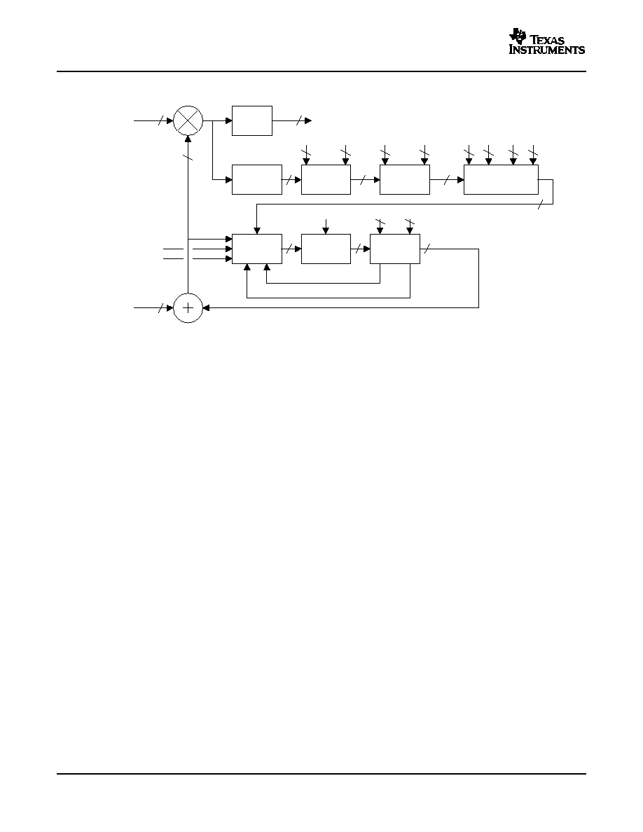
www.ti.com
PRODUCT PREVIEW
3.2.10
DDC AGC
limit &
round
18
24
12 integer &
12 fractional
I, Q
I, Q outputs (up to 25-bits in AGC bypass mode)
18
magnitude
compare
threshold
8
zero mask
4
under/over
detect
ucnt
8
ocnt
4
8
2
shift select
dsat
4
2
dzro
4
dabv
4
dblw
4
24
Gain
shift
29
accumulate
29
limit
24
Freeze
(from register bit
amin
16
amax
16
gain adjust
min limit
max limit
clear
5
S=+/-1, D=4-bit shift
Freeze
(from sync source)
GC5018
8-CHANNEL WIDEBAND RECEIVER
SLWS169 ≠ MAY 2005
The GC5018 automatic gain control circuit is shown above. The basic operation of the circuit is to multiply
the 18 bit input data from the PFIR by a 24-bit gain word that represents a gain or attenuation in the range
of 0 to 4096. The gain format is mixed integer and fraction. The 12-bit integer allows the gain to be
boosted by up to factor of 4096 (72 dB). The 12-bit fractional part allows the gain to be adjusted up or
down in steps of one part in 4096, or approximately 0.002 dB. If the integer portion is zero, then the circuit
attenuates the signal. The gain adjusted output data is saturated to full scale and then rounded to
between 4 and 18 bits in steps of one bit.
The AGC portion of the circuit is used to automatically adjust the gain so that the median magnitude of the
output data matches a target value, which is performed by comparing the magnitude of the output data
with a target threshold. If the magnitude is greater than the threshold, then the gain is decreased,
otherwise it is increased. The gain is adjusted as: G(t) = G + A(t), where G is the default, user supplied
gain value, and A(t) is the time varying adjustment. A(t) is updated as A(t) = A(t) + G(t)xSx2
≠D
, where S=1
if the magnitude is less than the threshold and is ≠1 if the magnitude exceeds the threshold, and where D
sets the adjustment step size. Note that the adjustment is a fraction of the current gain. This is designed to
set the AGC noise level to a known and acceptable level while keeping the AGC convergence and
tracking rate constant, independent of the gain level. The AGC noise will be equal to ±2
≠D
and the AGC
attack and decay rate will be exponential, with a time constant equal to 2
≠D
. Hence, the AGC will increase
or decrease by 0.63 times G(t) in 2
D
updates.
If one assumes the data is random with a Gaussian distribution, which is valid for UMTS if more than 12
users with different codes have been overlaid, then the relationship between the RMS level and the
median is MEDIAN = 0.6745xRMS, hence the threshold should be set to 0.6745 times the desired RMS
level.
The gain step size can be set using four different values of D, each of which is a 4 bit integer. D can range
from 3 to 18. The user can specify values of D for different situations, i.e., when the signal magnitude is
below the user-specified threshold (Dblw), is above the threshold (Dabv), is consistently equal to zero
(Dzro) or is consistently equal to maximum (Dsat). It is important to note that D represents a gain step
size. Smaller values of D represent larger gain steps. The definition of equal to zero is any number when
masked by zero_mask is considered to be zero. This permits consistently very small amplitude signals to
have their gain increased rapidly.
36
RECEIVE DIGITAL SIGNAL PROCESSING

www.ti.com
PRODUCT PREVIEW
AGC GAIN ERROR
0
1
2
3
4
5
6
7
1
10
100
1000
10000
100000
1000000
SAMPLES
D=3
D=4
D=5
D=6
D=7
D=8
D=9
D=10
D=11
D=12
D=13
D=14
D=15
D=16
D=17
D=18
D=18
D=3
GC5018
8-CHANNEL WIDEBAND RECEIVER
SLWS169 ≠ MAY 2005
Separate programmable D values allow the user to set different attack and decay time constants, and to
set shorter time constants for when the signal falls too low (equal to zero), or is too high (saturates). The
magnitude is considered to be consistently equal to zero by using a 4-bit counter that counts up every
time the 8-bit magnitude value is zero, and counts down otherwise. If the counter's value exceeds a user
specified threshold, then Dabv is used. Similarly the magnitude is considered too high by using a counter
that counts up when the magnitude is maximum, and counts down otherwise. If this counter exceeds
another user specified threshold, then Dsat is used.
As an example, if the AGC's current gain at a particular moment in time is 5.123, and the magnitude of the
signal is greater than zero, but less than the user-programmed threshold. Step size Dblw will be used to
modify the gain for the next sample. This represents the AGC attack profile. If Dblw is set to a value of 5,
then the gain for the next sample will be 5.123 + 5.123 x 2
≠5
= 5.123 + 0.160 = 5.283. If the signal's
magnitude is still less than the user-programmed threshold, then the gain for the next sample will be 5.283
+ 5.283 x 2
≠5
= 5.283 + 0.165 = 5.448. This continues until the signal's magnitude exceeds the
user-programmed threshold. When the magnitude exceeds threshold (but is not saturated), then step size
Dabv is automatically employed as a size rather than Dblw.
The AGC converges linearly in dB with a step size of 40log(1+2^-D) when the error is greater than 12 dB
(i.e. the gain is off by 12 dB or more). Within 6 dB the behavior is approximately a exponential decay with
a time constant of 2^(D-0.5) samples.
The suggested value of D is 5 or 6 when the error is greater than 12dB (i.e., in the fast range detected by
consistently zero or saturated data). This gives a step size of 0.5 or 0.25 dB per sample.
The suggested value when the gain is off by less than 12 dB is D=10, giving a exponential time constant
for delay of around 724 samples (63% decay every 724 samples).
The AGC noise once the AGC has converged is a random error of amplitude ±2^-D relative to the RMS
signal level. This means that the error level is ≠6xD dB below the signal RMS level. At D=10 (≠60 dB) the
error is negligible. The plot above shows the AGC response for vales of D ranging from 3 to 18. Error dB
represents the distance the signal level is from the desired target threshold.
The AGC is also subject to user specified upper and lower adjustment limits. The AGC stops incrementing
the gain if the adjustment exceeds Amax. It stops decrementing the gain if the adjustment is less than
Amin.
RECEIVE DIGITAL SIGNAL PROCESSING
37
www.ti.com
PRODUCT PREVIEW
GC5018
8-CHANNEL WIDEBAND RECEIVER
SLWS169 ≠ MAY 2005
The input data is received with a valid flag that is high when a valid sample is received. For complex data
the I and Q samples are on the same data input line and are not treated independently. An adjustment is
made for the magnitude of the I sample, and then another adjustment is made for the Q sample.
The AGC operates on UMTS and CDMA data. When in UMTS mode the I and Q data are each used to
produce the AGC level. There is no separate I path gain and Q path gain. When in CDMA mode there are
separate gain levels for the Signal and Diversity I and Q data. The I and Q for A (or the Signal ) pair is
calculated and then the I' and Q' for the B (or Diversity) pair is calculated.
There is a freeze mode for holding the accumulator at its current level. This will put the AGC in a hold
mode using the user-programmed gain along with the current gain_adjust value. To only use the user
programmed gain value as the gain, set the freeze bit and then clear the accumulator. When using the
freeze bit the full 25 bit output is sent out of the AGC block to support transferring up to 25 bits when the
AGC is disabled.
For TDD applications, freeze mode can be controlled using a sync source. This allows rxsync_a/b/c/d to
be assigned as a AGC hold signal to keep the AGC from responding during the transmit interval and run
during the receive interval. The freeze register bit is logically Ored with the freeze sync source.
The current AGC gain and state can also be optionally output with the DDCs I and Q output data by
setting the gain_mon variable. When in this mode, the top 14 bits of the current AGC gain word are
appended to the 8 bit AGC-modified I and Q output data.
Output
Bits(17:10)
Bits(9:4)
Bits(3:2)
Bits(1:0)
I
I output data
Gain(23:16)
"00"
Q
Q output data
Gain(15:10)
AGC State(1:0)
"00"
PROGRAMMING
VARIABLE
DESCRIPTION
agc_dblw(3:0)
Below threshold gain. Sets the value of gain step size Dblw (data x current gain below threshold). Ranges from
3 to 18, and maps to a 4 bit field. For example: 3 = "0000", 4= "0001",
...
18= "1111"
agc_dabv(3:0)
Above threshold gain. Sets the value of gain step size Dabv (data x current gain above threshold). Ranges
from 3 to 18, and maps to a 4 bit field. For example: 3 = "0000", 4= "0001",
...
18= "1111"
agc_dzro(3:0)
Zero signal gain. Sets the value of gain step size Dzro (data x current gain consistently zero). Ranges from 3 to
18, and maps to a 4 bit field. For example: 3 = "0000", 4= "0001",
...
18= "1111"
agc_dsat (3:0)
Saturated signal gain. Sets the value of gain step size Dsat (data x current gain consistently saturated).
Ranges from 3 to 18, and maps to a 4 bit field. For example: 3 = "0000", 4= "0001",
...
18= "1111"
agc_zero_msk(3:0)
Masks the lower 4 bits of signal data so as to be considered zeros.
agc_md(3:0)
AGC rounding. 0000= 18 bits out, 1111= 3 bits out.
agc_thresh(7:0)
AGC threshold. Compared with magnitude of 8 bits of input x gain.
agc_rnd_disable
AGC rounding is disabled when this bit is set.
agc_freeze
The AGC gain adjustment updates are disable when set.
agc_clear
The AGC gain adjustment accumulator is cleared when set
agc_gaina(23:0)
24 bit gain word for DDC A
agc_gainb(23:0)
24 bit gain word for DDC B (in CDMA mode)
agc_zero_cnt(3:0)
When the AGC output (input x gain) is zero value this number of times, the shoft value is changed to
agc_dzero.
agc_max_cnt(3:0)
When the AGC output (input x gain) is zero value this number of times, the shift value is changed to agc_dsat.
agc_amax(15:0)
The maximum value that gain can be adjusted up to. Top 12 bits are integer, bottom 4 bits are fractional.
agc_amin(15:0)
The minimum value that gain can be adjusted down to. Top 12 bits are integer, bottom 4 bits are fractional.
gain_mon
When set, combines current AGC gain with I and Q data. The 18 bit output format thus becomes:
I Portion: 8 bits of AGC'd I data - Gain(23:16) - 00
Q Portion: 8 bits of AGC'd Q data - Gain(15:10) - Status(1:0) - 00.
38
RECEIVE DIGITAL SIGNAL PROCESSING

www.ti.com
PRODUCT PREVIEW
3.2.11
DDC Output Interface
rx_sync_out_X
rxout_X_a
rxout_X_b
rxout_X_c
rxout_X_d
Serial Outputs
I ch A
I ch B
Q ch A
Q ch B
I msb
I msb-1
Q msb
Q msb-1
CDMA
UMTS
I msb
I msb-1
I msb-2
I msb-3
double length
PFIR UMTS
sync
clkdiv
frame
strobe
delay
DDC Block
1 UMTS mode channel or
2 CDMA mode channels
4
2
Q msb
Q msb-1
Q msb-2
Q msb-3
four outputs from
adjacent DDC block
GC5018
8-CHANNEL WIDEBAND RECEIVER
SLWS169 ≠ MAY 2005
PROGRAMMING
VARIABLE
DESCRIPTION
Note: Bit 0 of Status, when set, indicates the data is saturated. Bit 1 of Status, when set, indicates the data is
zero.
ssel_agc_freeze(2:0)
Sync selection for freeze mode, 1 of 8 sources. This source is ORed with the freeze register bit
ssel_gain(2:0)
Sync selection for the double buffered agc_gaina and agc_gainb register.
ssel_ddc_agc(2:0)
Sync selection used to initialize the AGC, primarily for test purposes.
The baseband I/Q sample interface can be configured as serial or parallel formatted data. The serial
interface closely matches the GC5316 style interface. The parallel interface is provided to interface directly
to the TMS320TCI110 when delayed antenna streams used to implement channel estimation buffering
and/or transport format combination indicator (TFCI) buffering are not required.
3.2.11.1
Serial Output Interface
Each DDC block can be assigned four serial output data pins. These pins are used to transfer
downconverted I/Q baseband data out of the GC5018 for subsequent processing. The usage of these pins
changes depending on how the DDC block is configured.
When the block is configured for two CDMA channels, a pair of serial data pins provides separate I and Q
data output for the two DDC channels. Word size is selectable from 4 to 25 bits with the most significant
bit first.
When the DDC block is configured for a single UMTS channel, even and odd I and Q data drive the four
serial pins separately, most significant bit first.
Four serial pins each for I and Q data can be optionally employed (instead of two for I and two for Q) at
half the output rate. This would most likely be used when two DDC channels (2k and 2k + 1, k= 0 to 5) are
combined to support double-length PFIR filtering (a channel is sacrificed). Formatting for I data is then:
Imsb, Imsb-1, Imsb-2, Imsb-3. Q data formatting is: Qmsb, Qmsb-1, Qmsb-2, Qmsb-3.
The frame strobe signal provided on the rx_sync_out_X pins can be programmed to arrive from 0 to 3 bit
clocks early via a 2 bit control parameter. The frame interval can be programmed from 1 to 63 bits. A
programmable 4-bit clock divider circuit is used to specify the serial bit rate. The clock divider circuit is
synchronized using a sync block discussed later in this document.
RECEIVE DIGITAL SIGNAL PROCESSING
39

www.ti.com
PRODUCT PREVIEW
rxclk
rxsync_out_X
MSB
rxsync_X
Programmed bit time
(2 rxclk cycles for this example)
tsetup
thold
tpd
rxout_X_Y
rxsync_X can be a pulse or level - interface will generate periodic frame strobes using programmed frame sync interval
3 rxclk + 1 Programmed bit time
GC5018
8-CHANNEL WIDEBAND RECEIVER
SLWS169 ≠ MAY 2005
Programming the serial port clock divider requires some thought and depends upon the channel's overall
decimation ratio, frame sync interval, number of output bits, and CDMA-UMTS mode.
In general:
the serial clock divide ratio ◊ the frame sync interval = the total receive decimation
The relationship between the number of serial bits output, clock divide ratio, and overall decimation ratio
is:
CDMA: [overall decimation ◊ (pser_recv_8pin + 1) ] / (pser_recv_clkdiv + 1) > pser_recv_bits + 1
UMTS: 2 ◊ [overall decimation ◊ (pser_recv_8pin + 1) ] / (pser_recv_clkdiv + 1) > pser_recv_bits + 1
Decimation by 2 in the output interface can be achieved by setting the frame strobe interval and clock
divider to 1/2 the PFIR output rate. The serial interface samples the PFIR output each time the transfer
interval defined by these two settings has completed. The decimation moment can be controlled using the
rxsync_X input signal selected as the sync source for the serial interface.
The timing diagram below shows the DDC serial output timing.
PROGRAMMING
VARIABLE
DESCRIPTION
pser_recv_fsinvl(6:0)
Frame sync interval in bits
pser_recv_bits(4:0)
Number of data output bits - 1. i.e.: 10001= 18 bits
pser_recv_clkdiv(3:0)
Receive serial interface clock divider rate ≠ 1.
0= rcclk, 15= rxclk/16
pser_recv_8pin
When set, configures the serial out pins for 4I and 4Q in UMTS mode. When clear, the mode is 2I and
2Q. Used in conjunction with pser_recv_alt.
pser_recv_alt
When set, outputs Q data from adjacent DDC channel.
pser_recv_fsdel(1:0)
Number of bit clocks the frame sync is output early with respect to serial data.
ssel_serial(2:0)
Sync source selection, 1 of 8.
tristate(6:3)
Tristate controls for the rx_sync_out_X and rxout_X_X pins. Pins are in tristate when the tristate register
bits are set.
40
RECEIVE DIGITAL SIGNAL PROCESSING
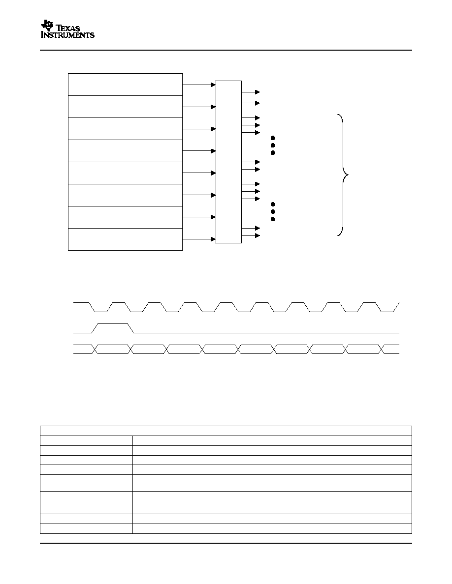
www.ti.com
PRODUCT PREVIEW
DDC0
DDC1
DDC2
DDC3
DDC4
DDC5
rx_sync_out_6
Output
format
rxclk _out
rxout_7_d
rxout_7_c
rxout_7_b
rxout_4_b
rxout_4_a
rxout_3_d
rxout_3_c
rxout_3_b
rxout_0_b
rxout_0_a
I(15)
I(14)
I(13)
I(1)
I(0)
Q(15)
Q(14)
Q(13)
Q(1)
Q(0)
rxclk _out
par_sync_out
Parallel I/Q
DDC6
DDC7
rxclk_out
par_sync_out
Parallel I/Q
IQ DDC0
IQ DDC1
IQ DDC2
IQ DDC3
IQ DDC4
IQ DDC5
IQ DDC6
IQ DDC7
GC5018
8-CHANNEL WIDEBAND RECEIVER
SLWS169 ≠ MAY 2005
3.2.11.2
Parallel Output Interface
When a parallel I/Q interface is required, a 32 bit time division multiplexed output mode can be selected
using the rxout_X_X pins. This interface is provided for direct connection to the TMS320TCI110 Receive
Chip Rate ASSP when delayed antenna streams are not required. The output sample rate, rxclk_out clock
polarity, par_sync_out position and number of channels to be output are all programmable.
The DDC channel serial interface synchronization source selections should all be programmed to the
same value when using this parallel output interface (each DDC channel ssel_serial(2:0) in the SYNC_0
register should be programmed to the same rxsync_A/B/C/D value).
Decimation by 2 in the output interface can be achieved by setting the frame strobe interval and clock
divider to 1/2 the PFIR output rate. The parallel interface samples the PFIR outputs each time the transfer
interval defined by these two settings has completed.
PROGRAMMING
VARIABLE
DESCRIPTION
par_recv_fsinvl(6:0)
rx_sync_out (frame strobe) sync interval. 0 is 1 rxclk cycle and 127 is 128 rxclk cycles.
par_recv_clkdiv(6:0)
rxclk_out cycles per IQ channel sample; 1 is full rate, 2 is rxclk/2, etc.
par_recv_chan(3:0)
Number channels to be output. 0 is 1 channel, and 15 is 16 channels.
par_recv_sync_del(6:0)
Delays the DDC0 pser sync source to establish the timing of IQ DDC0. Increasing the value delays the
par_sync_out location.
par_recv_syncout_del(3:0)
Delays the rx_sync_out position with respect to IQ DDC0. Setting to 0 moves the rx_sync_out pulse one
rxclk_out cycle before the IQ DDC0 word, setting to 1 places it as shown above, lined up with IQ DDC0,
etc.
par_recv_rxclk_pol
rxclk_out polarity. Outputs data on falling edges when cleared, rising edges when set.
par_recv_sync_pol
Parallel interface par_sync_out polarity. 0 is active low, 1 for active high
RECEIVE DIGITAL SIGNAL PROCESSING
41

www.ti.com
PRODUCT PREVIEW
3.2.12
DDC Checksum Generator
checksum
generator
0
initialized on sync event to "0000 0000 0000 0010"
rxclk
sync
1
2
3
12
rxout_X_a
14
rxout_X_b
13
11
10
rxout_X_c
rxout_X_d
9
rxout_X_a
rxout_X_b
rxout_X_c
rxout_X_d
15
16
results
register
checksum read-only
results updated on
each sync event
4
GC5018 GENERAL CONTROL
GC5018
8-CHANNEL WIDEBAND RECEIVER
SLWS169 ≠ MAY 2005
PROGRAMMING
VARIABLE
DESCRIPTION
par_recv_ena
Parallel TCI110 style interface enabled when set, serial interface enabled when cleared.
ssel_serial(2:0)
DDC channel serial interface sync source selection. All DDCs should be programmed to the same sync
source when using this parallel output interface.
gain_mon
When set, the parallel output data includes 8b I at I(15:8), 8b Q at Q(15:8), 14b AGC gain at I(7:0) and
Q(7:2) and 2b AGC state at Q(1:0).
tristate(6:3)
3-state controls for the rx_sync_out_X and rxout_X_X pins. Pins are in 3-state when the 3-state register
bits are set.
The checksum generator is used in conjunction with the input test signal generator to implement a self test
capability.
The sync for the checksum generator is internally connected to the ddc_counter output.
PROGRAMMING
VARIABLE
DESCRIPTION
ddc_chk_sum(15:0)
Read only DDC channel checksum results
The GC5018 is configured over a bi-directional 16 bit parallel data microprocessor control port. The
control port permits access to the control registers which configure the chip. The control registers are
organized using a paged-access scheme using 6 address lines. Half of the 64 addresses (Address 32
through Address 63) represent global registers. The other 32 (Address 0 through Address 31) are paged
resisters. This arrangement permits accessing a large number of control registers using relatively few
address lines.
Global registers (Address 32 through Address 63) are used to read/write GC5018 parameters that are
global in nature and can benefit from single read/write operations. Examples include chip status, reset,
sync options, checksum ramp parameters, interrupt sources, interrupt masks, 3-state controls and the
page register.
42
GC5018 GENERAL CONTROL
www.ti.com
PRODUCT PREVIEW
4.1
Microprocessor Interface Control Data, Address, and Strobes
4.1.1
MPU Timing Diagrams
tREC
tCSU
tHIZ
tCDLY
tCOH
ce_n
wr_n
rd_n
a[5:0]
d[15:0]
tREC
tCSU
tHIZ
tCDLY
valid data
tCOH
GC5018
8-CHANNEL WIDEBAND RECEIVER
SLWS169 ≠ MAY 2005
Global Address 33 is the page register. Writing a 16 bit value to this register sets the page to which future
write or read operations performed. These paged-registers contain the actual parameters that configure
the chip and are accessed by writing/reading address 0 through address 31.
The global 3-state register can be used to 3-state the output drivers on the GC5018, and also includes the
capability of disabling the chip's internal rxclk.
PROGRAMMING
VARIABLE
DESCRIPTION
rxclk_ena
Enables the internal rxclk when set. When cleared, the GC5018 will ignore the rxclk input signal and
hold the internal clock low.
3-state(10:0)
Various output pins are forced into tristate mode when these bits are asserted. See the GBL_3-STATE
register description for pin groups to bit assignments.
arst_func
When asserted, the internal datapath is held reset. The control register programming is not affected.
The microprocessor control bus consists of 16 bi-directional control data lines d[15:0], 6 address lines
a[5:0], a read enable line rd_n, a write enable line wr_n, and a chip enable line ce_n. These lines usually
interface to a microprocessor or DSP chip and is intended to look like a block of memory.
The interface can be operated in a 3 pin control mode (using rd_n, wr_n and ce_n) or 2 pin control mode
(using wr_n and ce_n with rd_n always low).
Figure 4-1. Read Operation ≠ 3 pin control mode
GC5018 GENERAL CONTROL
43
www.ti.com
PRODUCT PREVIEW
tREC
tCSU
tHIZ
tCDLY
tCOH
ce_n
wr_n
a[5:0]
d[15:0]
tREC
tCSU
tHIZ
tCDLY
valid data
tCOH
tREC
tCSU
t EWCSU
tCSPW
t CHD
ce_n
wr_n
a[5:0]
d[15:0]
tREC
tCSU
t
tC
valid data
t
rd_n
GC5018
8-CHANNEL WIDEBAND RECEIVER
SLWS169 ≠ MAY 2005
Figure 4-2. Read Operation ≠ 2 pin control mode (rd_n tied low)
Figure 4-3. Write Operation ≠ 3 pin control mode
44
GC5018 GENERAL CONTROL

www.ti.com
PRODUCT PREVIEW
tREC
tCSU
t EWCSU
tCSPW
t CHD
ce_n
wr_n
a[5:0]
d[15:0]
tREC
tCSU
t
tC
valid data
t
4.2
Synchronization Signals
GC5018
8-CHANNEL WIDEBAND RECEIVER
SLWS169 ≠ MAY 2005
Figure 4-4. Write Operation ≠ 2 pin control mode (rd_n tied low)
Various function blocks within the GC5018 need to be synchronized in order to realize predictable results.
The GC5018 provides a flexible system where each function block that requires synchronization can be
independently synchronized from either device pins or from a software "one-shot". The one-shot option is
setup and triggered through control registers. The four sync input pins, rxsync_a, rxsync_b, rxsync_c and
rxsync_d are qualified on the rxclk rising clock edge.
Table 4-1
shows the different sync modes available.
Table 4-1. Different Sync Modes Available
SYNC SELECT CODE
RECEIVE SYNC SOURCE
000
rxsync_a
001
rxsync_b
010
rxsync_c
011
rxsync_d
100
ddc sync counter terminal count
101
ddc sync triggered by s/w oneshot (register bit)
110
0 (always off)
111
1 (always on)
Table 4-2
and
Table 4-3
summarizes the blocks which have functions that can be synchronized using the
above eight sync source options.
Table 4-2. Receive Common Syncs
Sync Name
Purpose
sync_ddc_counter
Initializes the receive sync counter
sync_ddc
Initializes the receive ADC interface and clock generation circuits
sync_rxsync_out
selects sync signal to be output on the rx_sync_out pin.
sync_adc_fifo
Initializes the input and output pointers in the ADC fifo circuits.
sync_tst_decim
Initializes the testbus decimation counter.
GC5018 GENERAL CONTROL
45
www.ti.com
PRODUCT PREVIEW
4.3
Interrupt Handling
GC5018
8-CHANNEL WIDEBAND RECEIVER
SLWS169 ≠ MAY 2005
Table 4-2. Receive Common Syncs (continued)
Sync Name
Purpose
sync_recv_pmeterX
Initializes the rxin power meters. {X = 0,1,2 or 3}
sync_ragc_interval_X
Initializes the rxin receive AGC timers. {X = 0,1,2 or 3}
sync_ragc_freeze_X
rxin receive AGC freeze mode control. {X = 0,1,2 or 3}
sync_ragc_clear_X
Initializes the receive AGC error accumulator. {X = 0,1,2 or 3}
Table 4-3. DDC Channel Syncs
Sync Name
Purpose
sync_ddc_tadj
Selects zero stuff moment in the tadj fine adjustment section.
sync_ddc_tadj_reg
Updates the tadj output pointer register delay in the tadj coarse adjustment section.
sync_ddc_nco
Resets the NCO accumulator.
sync_ddc_freq
Updates the NCO freq registers.
sync_ddc_phase
Updates the NCO phase register.
sync_ddc_dither
Initializes the NCO dither circuits.
sync_ddc_cic
Selects the CIC decimation moment.
sync_ddc_pmeter
Initializes the receive channel power meters.
sync_ddc_gain
Updates the DDC channel AGC gain registers
sync_ddc_agc
Initializes the AGC accumulator.
sync_ddc_agc_freeze
AGC freeze mode control.
sync_ddc_serial
Initializes the receive serial interface.
A 32-bit general purpose timer is included in the synchronization function. The timer loads the user
programmed terminal count on a sync event, and counts down to zero using rxclk. The width of the
terminal count pulse can also be programmed up to rxclk cycles. The timers output can be used as a sync
source for any other circuits requiring a sync if desired, and can also be routed to the rx_sync_out pin.
PROGRAMMING
VARIABLE
DESCRIPTION
ddc_counter(31:0)
32-bit programmable terminal count
ddc_counter_width(7:0)
8-bit programmable terminal count pulse width
ssel_ddc_counter(2:0)
Sync source selection for the ddc counter
ssel_rxsync_out(2:0)
Sync source selection for the rx_sync_out pin
3-state(0)
When set, the interrupt and rx_sync_out pins are 3-stated.
rx_oneshot
Register bit used to generate the S/W oneshot signal for sync. This bit must be programmed from
cleared to set in order to generate a rising edge sync signal.
When a GC5018 block sets an interrupt, the interrupt pin will go active if the interrupt source is not
masked. The microprocessor should then read the interrupt register to determine the source of the
interrupt. The microprocessor will then have to write the interrupt register to clear the interrupt pin and the
interrupt source. The interrupt register and interrupt mask are located in the global registers section of the
control registers.
The GC5018 has 16 interrupt sources; power meters in each of the eight DDC blocks, power meters in the
four receive input interface, and four rxin_X_ovr (adc overflow) input pins where X={a,b,c,d}.
46
GC5018 GENERAL CONTROL
www.ti.com
PRODUCT PREVIEW
4.4
GC5018 Programming
GC5018
8-CHANNEL WIDEBAND RECEIVER
SLWS169 ≠ MAY 2005
PROGRAMMING
VARIABLE
DESCRIPTION
pmeterX_im(7:0)
Channel pmeter interrupt mask bits. Interrupt source is masked when set.
recv_pmeterX_im(3:0)
Receive input power meter interrupt masks.
rxin_X_ovr_im
ADC overflow input pin interrupt masks.
pmeterX(7:0)
Channel pmeter interrupt status.
recv_pmeterX(3:0)
Receive input power meter interrupt status.
rxin_X_ovr
ADC overflow input pin interrupt status.
intr_clr
When asserted, holds all interrupt status bits cleared. The interrupt pin will be inactive (always low) when this
bit is set. Intended for lab/debug use only
3-state(0)
When set, the interrupt and rx_sync_out pins are 3-stated.
The GC5018 includes over 3000 internal configuration registers and therefore implements a paged
addressing scheme. The register map includes a global control variables register address space that is
accessed directly when the a5 signal is high. This global control variables address space includes the
page register. All other registers are addressed using a combination of an address comprised of the
internal page register contents and the 6-bit external address; a5, a4, a3, a2, a1 and a0.
The page register is accessed when the 6-bit address a5:a0 is 0x21 (or binary "100001").
Page Register
Address
Registers Addressed With 5 Bit Address Space, Pins (a4:a0)
Contents in Hex
Pin a5
don't care
1
Global Control Variables 0x00 through 0x1F
0x0000
0
DDC0 PFIR taps 0 through 31 coefficient lsbs (1:0)
0x0020
0
DDC0 PFIR taps 32 through 63 coefficient lsbs (1:0)
0x0040
0
DDC0 PFIR taps 0 through 31 coefficient msbs (17:2)
0x0060
0
DDC0 PFIR taps 32 through 63 coefficient msbs (17:2)
0x0080
0
DDC0 CFIR taps 0 through 31 coefficient lsbs (1:0)
0x00A0
0
DDC0 CFIR taps 32 through 63 coefficient lsbs (1:0)
0x00C0
0
DDC0 CFIR taps 0 through 31 coefficient msbs (17:2)
0x00E0
0
DDC0 CFIR taps 32 through 63 coefficient msbs (17:2)
0x0100
0
DDC0 Control Registers 0x00 through 0x1F
0x0120
0
DDC0 Control Registers 0x20 through 0x3F
0x0200
0
DDC1 PFIR taps 0 through 31 coefficient lsbs (1:0)
0x0220
0
DDC1 PFIR taps 32 through 63 coefficient lsbs (1:0)
0x0240
0
DDC1 PFIR taps 0 through 31 coefficient msbs (17:2)
0x0260
0
DDC1 PFIR taps 32 through 63 coefficient msbs (17:2)
0x0280
0
DDC1 CFIR taps 0 through 31 coefficient lsbs (1:0)
0x02A0
0
DDC1 CFIR taps 32 through 63 coefficient lsbs (1:0)
0x02C0
0
DDC1 CFIR taps 0 through 31 coefficient msbs (17:2)
0x02E0
0
DDC1 CFIR taps 32 through 63 coefficient msbs (17:2)
0x0300
0
DDC1 Control Registers 0x00 through 0x1F
0x0320
0
DDC1 Control Registers 0x20 through 0x3F
0x0400
0
DDC2 PFIR taps 0 through 31 coefficient lsbs (1:0)
0x0420
0
DDC2 PFIR taps 32 through 63 coefficient lsbs (1:0)
GC5018 GENERAL CONTROL
47

www.ti.com
PRODUCT PREVIEW
GC5018
8-CHANNEL WIDEBAND RECEIVER
SLWS169 ≠ MAY 2005
Page Register
Address
Registers Addressed With 5 Bit Address Space, Pins (a4:a0)
Contents in Hex
Pin a5
0x0440
0
DDC2 PFIR taps 0 through 31 coefficient msbs (17:2)
0x0460
0
DDC2 PFIR taps 32 through 63 coefficient msbs (17:2)
0x0480
0
DDC2 CFIR taps 0 through 31 coefficient lsbs (1:0)
0x04A0
0
DDC2 CFIR taps 32 through 63 coefficient lsbs (1:0)
0x04C0
0
DDC2 CFIR taps 0 through 31 coefficient msbs (17:2)
0x04E0
0
DDC2 CFIR taps 32 through 63 coefficient msbs (17:2)
0x0500
0
DDC2 Control Registers 0x00 through 0x1F
0x0520
0
DDC2 Control Registers 0x20 through 0x3F
0x0600
0
DDC3 PFIR taps 0 through 31 coefficient lsbs (1:0)
0x0620
0
DDC3 PFIR taps 32 through 63 coefficient lsbs (1:0)
0x0640
0
DDC3 PFIR taps 0 through 31 coefficient msbs (17:2)
0x0660
0
DDC3 PFIR taps 32 through 63 coefficient msbs (17:2)
0x0680
0
DDC3 CFIR taps 0 through 31 coefficient lsbs (1:0)
0x06A0
0
DDC3 CFIR taps 32 through 63 coefficient lsbs (1:0)
0x06C0
0
DDC3 CFIR taps 0 through 31 coefficient msbs (17:2)
0x06E0
0
DDC3 CFIR taps 32 through 63 coefficient msbs (17:2)
0x0700
0
DDC3 Control Registers 0x00 through 0x1F
0x0720
0
DDC3 Control Registers 0x20 through 0x3F
0x0800
0
DDC4 PFIR taps 0 through 31 coefficient lsbs (1:0)
0x0820
0
DDC4 PFIR taps 32 through 63 coefficient lsbs (1:0)
0x0840
0
DDC4 PFIR taps 0 through 31 coefficient msbs (17:2)
0x0860
0
DDC4 PFIR taps 32 through 63 coefficient msbs (17:2)
0x0880
0
DDC4 CFIR taps 0 through 31 coefficient lsbs (1:0)
0x08A0
0
DDC4 CFIR taps 32 through 63 coefficient lsbs (1:0)
0x08C0
0
DDC4 CFIR taps 0 through 31 coefficient msbs (17:2)
0x08E0
0
DDC4 CFIR taps 32 through 63 coefficient msbs (17:2)
0x0900
0
DDC4 Control Registers 0x00 through 0x1F
0x0920
0
DDC4 Control Registers 0x20 through 0x3F
0x0A00
0
DDC5 PFIR taps 0 through 31 coefficient lsbs (1:0)
0x0A20
0
DDC5 PFIR taps 32 through 63 coefficient lsbs (1:0)
0x0A40
0
DDC5 PFIR taps 0 through 31 coefficient msbs (17:2)
0x0A60
0
DDC5 PFIR taps 32 through 63 coefficient msbs (17:2)
0x0A80
0
DDC5 CFIR taps 0 through 31 coefficient lsbs (1:0)
0x0AA0
0
DDC5 CFIR taps 32 through 63 coefficient lsbs (1:0)
0x0AC0
0
DDC5 CFIR taps 0 through 31 coefficient msbs (17:2)
0x0AE0
0
DDC5 CFIR taps 32 through 63 coefficient msbs (17:2)
0x0B00
0
DDC5 Control Registers 0x00 through 0x1F
0x0B20
0
DDC5 Control Registers 0x20 through 0x3F
0x0C00
0
DDC6 PFIR taps 0 through 31 coefficient lsbs (1:0)
0x0C20
0
DDC6 PFIR taps 32 through 63 coefficient lsbs (1:0)
0x0C40
0
DDC6 PFIR taps 0 through 31 coefficient msbs (17:2)
0x0C60
0
DDC6 PFIR taps 32 through 63 coefficient msbs (17:2)
0x0C80
0
DDC6 CFIR taps 0 through 31 coefficient lsbs (1:0)
48
GC5018 GENERAL CONTROL

www.ti.com
PRODUCT PREVIEW
GC5018
8-CHANNEL WIDEBAND RECEIVER
SLWS169 ≠ MAY 2005
Page Register
Address
Registers Addressed With 5 Bit Address Space, Pins (a4:a0)
Contents in Hex
Pin a5
0x0CA0
0
DDC6 CFIR taps 32 through 63 coefficient lsbs (1:0)
0x0CC0
0
DDC6 CFIR taps 0 through 31 coefficient msbs (17:2)
0x0CE0
0
DDC6 CFIR taps 32 through 63 coefficient msbs (17:2)
0x0D00
0
DDC6 Control Registers 0x00 through 0x1F
0x0D20
0
DDC6 Control Registers 0x20 through 0x3F
0x0E00
0
DDC7 PFIR taps 0 through 31 coefficient lsbs (1:0)
0x0E20
0
DDC7 PFIR taps 32 through 63 coefficient lsbs (1:0)
0x0E40
0
DDC7 PFIR taps 0 through 31 coefficient msbs (17:2)
0x0E60
0
DDC7 PFIR taps 32 through 63 coefficient msbs (17:2)
0x0E80
0
DDC7 CFIR taps 0 through 31 coefficient lsbs (1:0)
0x0EA0
0
DDC7 CFIR taps 32 through 63 coefficient lsbs (1:0)
0x0EC0
0
DDC7 CFIR taps 0 through 31 coefficient msbs (17:2)
0x0EE0
0
DDC7 CFIR taps 32 through 63 coefficient msbs (17:2)
0x0F00
0
DDC7 Control Registers 0x00 through 0x1F
0x0F20
0
DDC7 Control Registers 0x20 through 0x3F
0x1000
0
Receive Input AGC0 Error RAM addresses 0 through 31
0x1020
0
Receive Input AGC0 Error RAM addresses 32 through 63
0x1040
0
Receive Input AGC0 DVGA RAM addresses 0 through 31
0x1080
0
Receive Input AGC0 Gain RAM addresses 0 through 31
0x10A0
0
Receive Input AGC0 Gain RAM addresses 32 through 63
0x1100
0
Receive Input AGC1 Error RAM addresses 0 through 31
0x1120
0
Receive Input AGC1 Error RAM addresses 32 through 63
0x1140
0
Receive Input AGC1 DVGA RAM addresses 0 through 31
0x1180
0
Receive Input AGC1 Gain RAM addresses 0 through 31
0x11A0
0
Receive Input AGC1 Gain RAM addresses 32 through 63
0x1400
0
Receive Input AGC2 Error RAM addresses 0 through 31
0x1420
0
Receive Input AGC2 Error RAM addresses 32 through 63
0x1440
0
Receive Input AGC2 DVGA RAM addresses 0 through 31
0x1480
0
Receive Input AGC2 Gain RAM addresses 0 through 31
0x14A0
0
Receive Input AGC2 Gain RAM addresses 32 through 63
0x1500
0
Receive Input AGC3 Error RAM addresses 0 through 31
0x1520
0
Receive Input AGC3 Error RAM addresses 32 through 63
0x1540
0
Receive Input AGC3 DVGA RAM addresses 0 through 31
0x1580
0
Receive Input AGC3 Gain RAM addresses 0 through 31
0x15A0
0
Receive Input AGC3 Gain RAM addresses 32 through 63
0x1800
0
Receive Input Control Registers 0x00 through 0x1F
0x1820
0
Receive Input Control Registers 0x20 through 0x3F
0x1840
0
Receive Input AGC Control Registers 0x00 through 0x1F
0x1860
0
Receive Input AGC Control Registers 0x20 through 0x3F
49
GC5018 GENERAL CONTROL

www.ti.com
PRODUCT PREVIEW
4.4.1
Control Register Index
GC5018
8-CHANNEL WIDEBAND RECEIVER
SLWS169 ≠ MAY 2005
Table 4-4. Control Register Index
REGISTER NAME
SECTION
REGISTER NAME
SECTION
REGISTER NAME
SECTION
AGC_AMAX
Sec-
RAGC0_CLIP_SAMPLES
Sec-
RAGC3_SD_THRESH
Sec-
tion 4.4.5.23
tion 4.4.4.16
tion 4.4.4.48
AGC_AMIN
Sec-
RAGC0_CONFIG0
Sec-
RAGC3_SD_TIMER
Sec-
tion 4.4.5.24
tion 4.4.4.7
tion 4.4.4.49
AGC_CONFIG1
Sec-
RAGC0_CONFIG1
Sec-
RECV_CONFIG0
Sec-
tion 4.4.5.17
tion 4.4.4.8
tion 4.4.3.5
AGC_CONFIG2
Sec-
RAGC0_INTEGINVL_LSB
Sec-
RECV_CONFIG1
Sec-
tion 4.4.5.18
tion 4.4.4.5
tion 4.4.3.6
AGC_CONFIG3
Sec-
RAGC0_INTEGINVL_MSB
Sec-
RECV_PMETER_SYNC
Sec-
tion 4.4.5.19
tion 4.4.4.6
tion 4.4.3.8
AGC_GAINA
Sec-
RAGC0_SD_SAMPLES
Sec-
RECV_PMETER0_CONFIG
Sec-
tion 4.4.5.21
tion 4.4.4.11
tion 4.4.3.12
AGC_GAINB
Sec-
RAGC0_SD_THRESH
Sec-
RECV_PMETER0_LMSB
Sec-
tion 4.4.5.22
tion 4.4.4.9
tion 4.4.3.28
AGC_GAINMSB
Sec-
RAGC0_SD_TIMER
Sec-
RECV_PMETER0_LSB
Sec-
tion 4.4.5.20
tion 4.4.4.10
tion 4.4.3.26
CIC_MODE1
Sec-
RAGC1_ACCUM_LSB
Sec-
RECV_PMETER0_MID
Sec-
tion 4.4.5.5
tion 4.4.4.59
tion 4.4.3.27
CIC_MODE2
Sec-
RAGC1_ACCUM_MSB
Sec-
RECV_PMETER0_SQR_SUM
Sec-
tion 4.4.5.6
tion 4.4.4.60
_LSB
tion 4.4.3.9
CONFIG
Sec-
RAGC1_CLIP_ERROR
Sec-
RECV_PMETER0_STRT_INT
Sec-
tion 4.4.2.3
tion 4.4.4.30
VL_LSB
tion 4.4.3.10
CONFIG1
Sec-
RAGC1_CLIP_HITHRESH
Sec-
RECV_PMETER0_SYNC_DL
Sec-
tion 4.4.5.15
tion 4.4.4.25
Y
tion 4.4.3.11
CONFIG2
Sec-
RAGC1_CLIP_HITIMER
Sec-
RECV_PMETER0_UMSB
Sec-
tion 4.4.5.16
tion 4.4.4.27
tion 4.4.3.29
DDC_CHK_SUM
Sec-
RAGC1_CLIP_LOTHRESH
Sec-
RECV_PMETER1_CONFIG
Sec-
tion 4.4.5.31
tion 4.4.4.26
tion 4.4.3.16
DDCCONFIG1
Sec-
RAGC1_CLIP_LOTIMER
Sec-
RECV_PMETER1_LMSB
Sec-
tion 4.4.5.27
tion 4.4.4.28
tion 4.4.3.32
FIR_GAIN
Sec-
RAGC1_CLIP_SAMPLES
Sec-
RECV_PMETER1_LSB
Sec-
tion 4.4.5.2
tion 4.4.4.29
tion 4.4.3.30
FIR_MODE
Sec-
RAGC1_CONFIG0
Sec-
RECV_PMETER1_MID
Sec-
tion 4.4.5.1
tion 4.4.4.20
tion 4.4.3.31
GBL_IMASK0
Sec-
RAGC1_CONFIG1
Sec-
RECV_PMETER1_SQR_SUM
Sec-
tion 4.4.2.8
tion 4.4.4.21
_LSB
tion 4.4.3.13
GBL_INTERRUPT0
Sec-
RAGC1_INTEGINVL_LSB
Sec-
RECV_PMETER1_STRT_INT
Sec-
tion 4.4.2.9
tion 4.4.4.18
VL_LSB
tion 4.4.3.14
GBL_ONESHOT
Sec-
RAGC1_INTEGINVL_MSB
Sec-
RECV_PMETER1_SYNC_DL
Sec-
tion 4.4.2.7
tion 4.4.4.19
Y
tion 4.4.3.15
GBL_PAR_CONFIG0
Sec-
RAGC1_SD_SAMPLES
Sec-
RECV_PMETER1_UMSB
Sec-
tion 4.4.2.4
tion 4.4.4.24
tion 4.4.3.33
GBL_PAR_CONFIG1
Sec-
RAGC1_SD_THRESH
Sec-
RECV_PMETER2_CONFIG
Sec-
tion 4.4.2.5
tion 4.4.4.22
tion 4.4.3.20
GBL_TRISTATE
Sec-
RAGC1_SD_TIMER
Sec-
RECV_PMETER2_LMSB
Sec-
tion 4.4.2.6
tion 4.4.4.23
tion 4.4.3.36
NZ_PWR_MASK
Sec-
RAGC2_ACCUM_LSB
Sec-
RECV_PMETER2_LSB
Sec-
tion 4.4.3.7
tion 4.4.4.61
tion 4.4.3.34
PAGE
Sec-
RAGC2_ACCUM_MSB
Sec-
RECV_PMETER2_MID
Sec-
tion 4.4.2.2
tion 4.4.4.62
tion 4.4.3.35
50
GC5018 GENERAL CONTROL

www.ti.com
PRODUCT PREVIEW
GC5018
8-CHANNEL WIDEBAND RECEIVER
SLWS169 ≠ MAY 2005
Table 4-4. Control Register Index (continued)
REGISTER NAME
SECTION
REGISTER NAME
SECTION
REGISTER NAME
SECTION
PHASE_OFFSETA
Sec-
RAGC2_CLIP_ERROR
Sec-
RECV_PMETER2_SQR_SUM
Sec-
tion 4.4.5.13
tion 4.4.4.43
_LSB
tion 4.4.3.17
PHASE_OFFSETB
Sec-
RAGC2_CLIP_HITHRESH
Sec-
RECV_PMETER2_STRT_INT
Sec-
tion 4.4.5.14
tion 4.4.4.38
VL_LSB
tion 4.4.3.18
PHASEADD0A
Sec-
RAGC2_CLIP_HITIMER
Sec-
RECV_PMETER2_SYNC_DL
Sec-
tion 4.4.5.9
tion 4.4.4.40
Y
tion 4.4.3.19
PHASEADD0B
Sec-
RAGC2_CLIP_LOTHRESH
Sec-
RECV_PMETER2_UMSB
Sec-
tion 4.4.5.11
tion 4.4.4.39
tion 4.4.3.37
PHASEADD1A
Sec-
RAGC2_CLIP_LOTIMER
Sec-
RECV_PMETER3_CONFIG
Sec-
tion 4.4.5.10
tion 4.4.4.41
tion 4.4.3.24
PHASEADD1B
Sec-
RAGC2_CLIP_SAMPLES
Sec-
RECV_PMETER3_LMSB
Sec-
tion 4.4.5.12
tion 4.4.4.42
tion 4.4.3.40
PMETER_RESULT_A_LSB
Sec-
RAGC2_CONFIG0
Sec-
RECV_PMETER3_LSB
Sec-
tion 4.4.5.32
tion 4.4.4.33
tion 4.4.3.38
PMETER_RESULT_A_MID
Sec-
RAGC2_CONFIG1
Sec-
RECV_PMETER3_MID
Sec-
tion 4.4.5.33
tion 4.4.4.34
tion 4.4.3.39
PMETER_RESULT_A_MSB
Sec-
RAGC2_INTEGINVL_LSB
Sec-
RECV_PMETER3_SQR_SUM
Sec-
tion 4.4.5.34
tion 4.4.4.31
_LSB
tion 4.4.3.21
PMETER_RESULT_B_LSB
Sec-
RAGC2_INTEGINVL_MSB
Sec-
RECV_PMETER3_STRT_INT
Sec-
tion 4.4.5.35
tion 4.4.4.32
VL_LSB
tion 4.4.3.22
PMETER_RESULT_B_MID
Sec-
RAGC2_SD_SAMPLES
Sec-
RECV_PMETER3_SYNC_DL
Sec-
tion 4.4.5.36
tion 4.4.4.37
Y
tion 4.4.3.23
PMETER_RESULT_B_MSB
Sec-
RAGC2_SD_THRESH
Sec-
RECV_PMETER3_UMSB
Sec-
tion 4.4.5.37
tion 4.4.4.35
tion 4.4.3.41
PMETER_RESULT_AB_UMS
Sec-
RAGC2_SD_TIMER
Sec-
RECV_SLF_TST_VALUE
Sec-
B
tion 4.4.5.38
tion 4.4.4.36
tion 4.4.3.25
PSER_CONFIG1
Sec-
RAGC3_ACCUM_LSB
Sec-
SQR_SUM
Sec-
tion 4.4.5.25
tion 4.4.4.63
tion 4.4.5.3
PSER_CONFIG2
Sec-
RAGC3_ACCUM_MSB
Sec-
SSEL_DDC_CNTR
Sec-
tion 4.4.5.26
tion 4.4.4.64
tion 4.4.3.3
RAGC_CONFIG0
Sec-
RAGC3_CLIP_ERROR
Sec-
SSEL_RX_0
Sec-
tion 4.4.4.1
tion 4.4.4.56
tion 4.4.3.4
RAGC_CONFIG1
Sec-
RAGC3_CLIP_HITHRESH
Sec-
STRT_INTRVL
Sec-
tion 4.4.4.2
tion 4.4.4.51
tion 4.4.5.4
RAGC_CONFIG2
Sec-
RAGC3_CLIP_HITIMER
Sec-
SYNC_0
Sec-
tion 4.4.4.3
tion 4.4.4.53
tion 4.4.5.28
RAGC_CONFIG3
Sec-
RAGC3_CLIP_LOTHRESH
Sec-
SYNC_1
Sec-
tion 4.4.4.4
tion 4.4.4.52
tion 4.4.5.29
RAGC0_ACCUM_LSB
Sec-
RAGC3_CLIP_LOTIMER
Sec-
SYNC_2
Sec-
tion 4.4.4.57
tion 4.4.4.54
tion 4.4.5.30
RAGC0_ACCUM_MSB
Sec-
RAGC3_CLIP_SAMPLES
Sec-
SYNC_DDC_CNTR_LSB
Sec-
tion 4.4.4.58
tion 4.4.4.55
tion 4.4.3.1
RAGC0_CLIP_ERROR
Sec-
RAGC3_CONFIG0
Sec-
SYNC_DDC_CNTR_MSB
Sec-
tion 4.4.4.17
tion 4.4.4.46
tion 4.4.3.2
RAGC0_CLIP_HITHRESH
Sec-
RAGC3_CONFIG1
Sec-
TADJC
Sec-
tion 4.4.4.12
tion 4.4.4.47
tion 4.4.5.7
RAGC0_CLIP_HITIMER
Sec-
RAGC3_INTEGINVL_LSB
Sec-
TADJF
Sec-
tion 4.4.4.14
tion 4.4.4.44
tion 4.4.5.8
RAGC0_CLIP_LOTHRESH
Sec-
RAGC3_INTEGINVL_MSB
Sec-
VER
Sec-
tion 4.4.4.13
tion 4.4.4.45
tion 4.4.2.1
RAGC0_CLIP_LOTIMER
Sec-
RAGC3_SD_SAMPLES
Sec-
tion 4.4.4.15
tion 4.4.4.50
GC5018 GENERAL CONTROL
51

www.ti.com
PRODUCT PREVIEW
4.4.2
Global Control Variables
GC5018
8-CHANNEL WIDEBAND RECEIVER
SLWS169 ≠ MAY 2005
Table 4-4. Control Register Index (continued)
REGISTER NAME
SECTION
REGISTER NAME
SECTION
REGISTER NAME
SECTION
These registers are accessed directly without page address extension; when pin a5 is high during a read
or write access, this block of 32 registers are accessed.
4.4.2.1
VER Register
Register name: VER
Address: 0x0
READ_ONLY
BIT 15
BIT 8
unused
unused
unused
unused
unused
unused
unused
unused
0
0
0
0
0
0
0
0
BIT 7
BIT 0
unused
unused
unused
unused
VER3
VER2
VER1
VER0
0
0
0
0
0
0
0
1
52
GC5018 GENERAL CONTROL

www.ti.com
PRODUCT PREVIEW
GC5018
8-CHANNEL WIDEBAND RECEIVER
SLWS169 ≠ MAY 2005
VER(3:0):
A hardwired read only register that returns the version of the chip.
4.4.2.2
PAGE Register
Register name: PAGE
Address: 0x1
BIT 15
BIT 8
unused
unused
unused
W(2:0)
X
Y(2)
0
0
0
0
0
0
0
0
BIT 7
BIT 0
Y(1)
Y(0)
Zp
unused
unused
unused
unused
unused
0
0
0
0
0
0
0
0
W(2:0) :
Selects which dual DDC block to address.
X :
The DDC modules are configured as dual DDCs; an even numbered DDC and odd
numbered DDC are contained in each dual DDC module, the X bit selects which DDC gets
address. (DDC0/2/4/6=0, DDC1/3/5/7=1)
W(2:0)
X bit
Selected Block
000
0
DDC0
000
1
DDC1
001
0
DDC2
001
1
DDC3
010
0
DDC4
010
1
DDC5
011
0
DDC6
011
1
DDC7
100
0
Receive AGC0/1 RAMs
101
0
Receive AGC2/3 RAMs
110
0
Receive Input Interface
Y(2:0) :
Within each major block, there are up to 8 different Zones that can be addressed using the Y
bits.
Y(2:0)
DDC Zone
Receive Input Interface Zone
Receive AGC RAMs Zone
000
PFIR coeffient lower 2 bits
CHIPS control registers
RAGC0/2 ERRMAP
001
PFIR coeffient upper 16 bits
RAGC control registers
RAGC0/2 DVGAMAP
010
CFIR coeffient lower 2 bits
Not assigned
RAGC0/2 GAINMAP
011
CFIR coeffient upper 16 bits
Not assigned
Not assigned
100
Control registers
Not assigned
RAGC1/3 ERRMAP
101
Not assigned
Not assigned
RAGC1/3 DVGAMAP
110
Not assigned
Not assigned
RAGC1/3 GAINMAP
111
Not assigned
Not assigned
Not assigned
Zp :
The Zp bit is the MSB of the address word sent to the registers and rams. This bit can be
thought of as an upper/lower selector of the 64 word addressing.
4.4.2.3
CONFIG Register
GC5018 GENERAL CONTROL
53

www.ti.com
PRODUCT PREVIEW
GC5018
8-CHANNEL WIDEBAND RECEIVER
SLWS169 ≠ MAY 2005
Register name: CONFIG
Address: 0x2
BIT 15
BIT 8
slf_ tst_ena
rduz_sens_ena
arst_ func
tst_rate_sel(4:0)
0
0
0
0
0
0
0
0
BIT 7
BIT 0
par_recv_ena
gbl_ ddc_write
intr_ clr
tst_select(3:0)
tst_ on
0
0
0
1
1
1
0
0
slf_tst_ena : Turns on the checksum LFSR for the receivers. They are located in the RECEIVE INPUT
INTERFACE and DDC blocks
rduz_sens_ena : When enabled, adds noise to the LSB's of the ADC inputs.
arst_func : When asserted, resets the functional portion of the circuits. The MPU registers do not get
reset and retain their programmed value
tst_rate_sel(4:0) : Sets the rate of the output test data and clock. The length of the clock cycle is the
value in tst_rate_sel+1 multiplied by the RXCLK period.
par_recv_ena : When asserted, the rxout_*_* serial pins join to form a 32 bit parallel output using 32 pins
as a data bus, one pin as a output clock and one pin as a sync. This is used to connect to
the TCI110 Chip rate processor from TI.
gbl_ddc_write : When asserted, the mpu writes are global. This means that DDC0/2/4/6 or DDC1/3/5/7
can be programmed simultaneously with the same values. This is an effort to reduce the
amount of time spent programming the device. A common setup can be used to program the
DDC0/2/4/6, then all the DDC1/3/5/7. Afterwards, just individual writes to the registers which
differ between DDCs can be done. To use this feature, this bit must be asserted and the
DDC0/1 must be addressed. Any other DDC address will not work.
intr_clr :
When asserted, this bit forces all interrupts to be cleared. To allow the interrupts to be set
again, this bit must be programmed to zero. This does not stop blocks from generating
interrupts, but rather just keeps the interrupts from being reported.
tst_select(3:0) : This selects which block the test output comes from:
tst_select(3:0)
Test Data Sent to Output
0000
DDC 0
0001
DDC 1
0010
DDC 2
0011
DDC 3
0100
DDC 4
0101
DDC 5
0110
DDC 6
0111
DDC 7
1000
rxin_a and rxin_b FIFO outputs
others
none selected
tst_on :
When asserted, the testbus is active. The ADC input ports rxin_c(15:0), rxin_d(15:0),
dvga_c(5:0) and dvga_d(5:0) become the testbus output ports. When this bit is set, the
rxin_c(15:0) and rxin_d(15:0) ports become chip outputs. The dvga_c(5:0) and dvga_d(5:0)
ports are enabled separately using the GBL_TRISTATE register
54
GC5018 GENERAL CONTROL

www.ti.com
PRODUCT PREVIEW
GC5018
8-CHANNEL WIDEBAND RECEIVER
SLWS169 ≠ MAY 2005
4.4.2.4
GBL_PAR_CONFIG0 Register
Register name: GBL_PAR_CONFIG0
Address: 0x3
BIT 15
BIT 8
par_recv_sync_del(6:0)
tst_clk_pol
0
0
0
0
0
0
0
0
BIT 7
BIT 0
par_recv_clkdiv(6:0)
par_recv_
rxclk_pol
0
0
0
0
0
0
0
0
par_recv_sync_del(6:0) : Delays the sync source from the DDC0 AGC output by (par_recv_sync_del+1)
rxclk cycles.
tst_clk_pol : Selects the polarity of the test clock output at dvga_c(1) when the test bus is enabled; 0 for
rising edge in the center of valid data, 1 for falling edge in the center of valid data. No effect
when tst_rate_sel is "00000".
par_recv_clkdiv(6:0) : Selects the parallel interface output clock rate.
par_recv_rxclk_pol : Selects the polarity of the rxclk_out clock output; 0 for rising edge in the center of
valid data, 1 for falling edge in the center of valid data.
4.4.2.5
GBL_PAR_CONFIG1 Register
Register name: GBL_PAR_CONFIG1
Address: 0x4
BIT 15
BIT 8
par_recv_syncout_del(3:0)
par_recv_chan(3:0)
0
0
0
0
0
0
0
0
BIT 7
BIT 0
par_recv_fsinvl(6:0)
par_recv_
sync_pol
0
0
0
0
0
0
0
0
par_recv_syncout_del(3:0) : Changes the rx_sync_out position with respect to IQ DDC0. Setting to 0
causes rx_sync_out to lead IQ DDC0 by 1 output sample, setting to 1 causes rx_sync_out to
line up with IQ DDC0, setting to 2 causes rx_sync_out to trail IQ DDC0 by 1 output sample,
etc.
par_recv_chan(3:0) : Selects the number of channels to be output over the parallel interface, from 1 to 16
channels.
par_recv_fsinvl(6:0) : Selects the number of rxclk cycles per parallel interface frame, from 1 to 128
cycles.
par_recv_sync_pol : Selects the polarity of the parallel interface sync pulse; 0 for active low, 1 for active
high.
4.4.2.6
GBL_TRISTATE Register
GC5018 GENERAL CONTROL
55
www.ti.com
PRODUCT PREVIEW
GC5018
8-CHANNEL WIDEBAND RECEIVER
SLWS169 ≠ MAY 2005
Register name: GBL_TRISTATE
Address: 0x5
BIT 15
BIT 8
rxclk_ena
unused
unused
unused
unused
tristate(10)
tristate(9)
tristate(8)
1
0
0
0
0
1
1
1
BIT 7
BIT 0
tristate(7)
tristate(6)
tristate(5)
tristate(4)
tristate(3)
tristate(2)
tristate(1)
1
1
1
1
1
1
1
1
rxclk_ena : Master rxclk enable. When set, the chip's rxclk is enabled, when cleared, rxclk is disabled.
All tristates are ACTIVE LOW so a `0' turns on the output and a `1' tristates it.
tristate(10) : This bit turns on the dvga_d outputs.
tristate(9) : This bit turns on the dvga_c outputs.
tristate(8) : This bit turns on the dvga_b outputs.
tristate(7) : This bit turns on the dvga_a outputs.
tristate(6) : This bit turns on the rx_sync_out_6/7, and the rxout_6/7_a/b/c/d outputs.
tristate(5) : This bit turns on the rx_sync_out_4/5, and the rxout_4/5_a/b/c/d outputs.
tristate(4) : This bit turns on the rx_sync_out_2/3, and the rxout_2/3_a/b/c/d outputs.
tristate(3) : This bit turns on the rx_sync_out_0/1, and the rxout_0/1_a/b/c/d outputs.
tristate(2) : TBD
tristate(1) : rxclk_out
tristate0) :
interrupt, and rx_sync_out.
4.4.2.7
GBL_ONESHOT Register
Register name: GBL_ONESHOT
Address: 0x6
BIT 15
BIT 8
unused
unused
unused
unused
unused
unused
unused
unused
0
0
0
0
0
0
0
0
BIT 7
BIT 0
rx_oneshot
unused
unused
unused
unused
unused
unused
unused
0
0
0
0
0
0
0
0
rx_oneshot : When set, a one shot pulse is sent to the receive blocks for syncing. This only works if the
blocks are programmed to use the oneshot as the sync source. To use the oneshot again, it
must be programmed back to a `0' and then back to a `1'.
4.4.2.8
GBL_IMASK0 Register
Register name: GBL_IMASK0
Address: 0x7
BIT 15
BIT 8
pmeter7_im
pmeter6_im
pmeter5_im
pmeter4_im
pmeter3_im
pmeter2_im
pmeter1_im
pmeter0_im
0
0
0
0
0
0
0
0
BIT 7
BIT 0
56
GC5018 GENERAL CONTROL
www.ti.com
PRODUCT PREVIEW
4.4.3
Receive Input Interface Controls
GC5018
8-CHANNEL WIDEBAND RECEIVER
SLWS169 ≠ MAY 2005
recv_
recv_
recv_
recv_
rxin_a_ ovr_im
rxin_b_ ovr_im
rxin_c_ ovr_im
rxin_d_ ovr_im
pmeter0_im
pmeter1_im
pmeter2_im
pmeter3_im
0
0
0
0
0
0
0
0
pmeterX_im : When asserted, masks the interrupt for the particular DDC pmeter, X= {0,1,2,3,4,5,6,7}.
recv_pmeterX_im : When asserted, masks the interrupt for the particular receive input pmeter, X=
{0,1,2,3 }.
rxin_X_ovr_im : When asserted, masks the interrupt for the particular rxin overflow, X={a,b,c,d}.
4.4.2.9
GBL_INTERRUPT0 Register
Register name: GBL_INTERRUPT0
Address: 0x9
BIT 15
BIT 8
pmeter7
pmeter6
pmeter5
pmeter4
pmeter3
pmeter2
pmeter1
pmeter0
0
0
0
0
0
0
0
0
BIT 7
BIT 0
recv_ pmeter0
recv_ pmeter1
recv_ pmeter2
recv_ pmeter3
rxin_a_ovr
rxin_b_ovr
rcin_c_ovr
rxin_d_ovr
0
0
0
0
0
0
0
0
pmeterX :
Asserted when an interrupt has been generated by this DDC pmeterX block, X={1,2,3,4,5,6,7
recv_pmeterX : Asserted when an interrupt has been generated by this receive input pmeter, X= {0,1,2,3
}.
rxin_X_ovr : Asserted when a logic high input from the rxin_X_ovr pin occurs, X={a,b,c,d}.
4.4.3.1
SYNC_DDC_CNTR_LSB Register
Register name: SYNC_DDC_CNTR_LSB
Address: 0x0
BIT 15
BIT 8
ddc_counter(15:8)
0
0
0
0
0
0
0
0
BIT 7
BIT 0
ddc_counter(7:0)
0
0
0
0
0
0
0
0
4.4.3.2
SYNC_DDC_CNTR_MSB
Register name: SYNC_DDC_CNTR_MSB
Address: 0x1
BIT 15
BIT 8
ddc_counter(31:24)
0
0
0
0
0
0
0
0
BIT 7
BIT 0
ddc_counter(23:16)
0
0
0
0
0
0
0
0
57
GC5018 GENERAL CONTROL

www.ti.com
PRODUCT PREVIEW
GC5018
8-CHANNEL WIDEBAND RECEIVER
SLWS169 ≠ MAY 2005
ddc_counter(32:0) : 32 bit interval timer common to all DDC sync inputs. This timer may be programmed
to any interval count, and each DDC synchronization input can select this counter as a
source. The value programmed into the counter is: (desired number ≠1). The counter
increments on each RX clock rising edge.
4.4.3.3
SSEL_DDC_CNTR Register
Register name: SSEL_DDC_CNTR
Address: 0x2
BIT 15
BIT 8
rxinab_mux
rxincd_mux
unused
unused
unused
ssel_ddc_counter(2:0)
0
0
0
0
0
0
0
0
BIT 7
BIT 0
ddc_counter_width(7:0)
0
0
0
0
0
0
0
0
rxinab_mux : When asserted, the rxin_a and rxin_b inputs are internally driven by the rxin_c and rxin_d
ports, respectively (Factory test use only).
rxincd_mux : When asserted, the rxin_c and rxin_d inputs are internally driven by the rxin_a and rxin_b
ports, respectively (Factory test use only).
ssel_ddc_counter(2:0) : Selects the sync source for the DDC sync counter.
ddc_counter_width(7:0) : Sets the width of the counter generated sync pulse in RX clock cycles, from 1
to 256.
Sync sources are contained in this and many of the following registers. For all sync source selections:
ssel_ddc_XXXXX(2:0)
Selected Sync Source
000
rxsyncA
001
rxsyncB
010
rxsyncC
011
rxsyncD
100
DDC sync counter
101
one shot (register write triggered)
110
always 0
111
always 1
4.4.3.4
SSEL_RX_0 Register
Register name: SSEL_RX_0
Address: 0x3
BIT 15
BIT 8
unused
ssel_adc_fifo(2:0)
unused
ssel_tst_decim(2:0)
0
0
0
0
0
0
0
0
BIT 7
BIT 0
unused
ssel_rxsync_out(2:0)
unused
ssel_ddc(2:0)
0
0
0
0
0
0
0
0
58
GC5018 GENERAL CONTROL
www.ti.com
PRODUCT PREVIEW
GC5018
8-CHANNEL WIDEBAND RECEIVER
SLWS169 ≠ MAY 2005
ssel_adc_fifo(2:0) : Selects the sync source for the adc FIFO blocks. Sync reinitializes the read and write
pointers of the FIFO.
ssel_tst_decim(2:0) : Selects the sync source for the test bus decimator block.
ssel_rxsync_out(2:0) : Selects the sync source for the RXSYNC_OUT pin.
ssel_ddc(2:0) : Selects the sync source for the DDC data input mux and mixer. Controls clock generation
in each DDC block (before the CIC input) which must match because the FIFO output clock
is common for all DDC blocks.
4.4.3.5
RECV_CONFIG0 Register
Register name: RECV_CONFIG0
Address: 0x4
BIT 15
BIT 8
rate_sel(1:0)
adc_
adc_
self_test_
adc_
ragc_mpu_ram
tst_ decim17
fifo_strap_ab
fifo_strap_cd
const_ena
fifo_bypass
_read
0
0
0
0
0
0
0
0
BIT 7
BIT 0
tst_decim_delay(3:0)
pmeter3_iq
pmeter2_iq
pmeter1_iq
pmeter0_iq
0
0
0
0
0
0
0
0
rate_sel(1:0) : Tells the RECV_CDRV the input rate. This is the rxin_a/b/c/d input rate and the rate that
the RECEIVE INPUT INTERFACE block sends data to the DDCs.
rate_sel
Input clock rate
00
rxclk
01
rxclk/2
10
rxclk/4
11
rxclk/8
adc_fifo_strap_ab : When asserted, the input pointers of the rxin_a FIFO and rxin_b FIFO are hooked
together in lock step configuration. This is used for maintaining FIFO delay consistency when
complex inputs are driven on rxin_a(I) and rxin_b(Q). rxin_a is the Master.
adc_fifo_strap_cd : When asserted, the input pointers of the rxin_c FIFO and rxin_d FIFO are hooked
together in lock step configuration. This is used for maintaining FIFO delay consistency when
complex inputs are driven on rxin_c(I) and rxin_d(Q). rxin_c is the Master.
self_test_const_ena : When asserted, (with slf_tst_ena also asserted), a constant value is output by the
test and noise generator instead of the pseudo random sequence. The constant value is
programmable.
adc_fifo_bypass : When asserted, the ADC FIFO circuits are bypassed. Input data is then clocked in
directly using the rxclk input. The ssel_ddc selection value will control the location of the
internally generated sample clock when this bit is asserted where rate_sel is rxclk/2, rxclk/4
or rxclk/8.
ragc_mpu_ram_read : When asserted, the RAMs in the RAGC blocks can be read. This bit should only
be set when reading the RAGC map rams via the mpu interface and must be cleared for
proper RAGC operation.
tst_decim17 : When set, the decimation factor of the tst_decimator block is 17X. When cleared, the
decimation factor is 16X if the fuse is blown, 1X (no decimation) with the fuse intact.
tst_decim_delay(3:0) : These bits set the delay from the sync occurring until the decimator samples. In
other words, the moment of the decimator is set by this delay value.
GC5018 GENERAL CONTROL
59

www.ti.com
PRODUCT PREVIEW
GC5018
8-CHANNEL WIDEBAND RECEIVER
SLWS169 ≠ MAY 2005
pmeter3_iq : When asserted, the pmeter3 block takes input from both rxin_c and rxin_d as a complex
sample pair. When de-asserted, only input from rxin_d is used for the power measurement.
pmeter2_iq : When asserted, the pmeter2 block takes input from both rxin_c and rxin_d as a complex
sample pair. When de-asserted, only input from rxin_c is used for the power measurement.
pmeter1_iq : When asserted, the pmeter1 block takes input from both rxin_a and rxin_b as a complex
sample pair. When de-asserted, only input from rxin_b is used for the power measurement.
pmeter0_iq : When asserted, the pmeter0 block takes input from both rxin_a and rxin_b as a complex
sample pair. When de-asserted, only input from rxin_a is used for the power measurement.
4.4.3.6
RECV_CONFIG1 Register
Register name: RECV_CONFIG1
Address: 0x5
BIT 15
BIT 8
msb_pos_d(2:0)
offset_bin_d
msb_pos_c(2:0)
offset_bin_c
0
0
0
0
0
0
0
0
BIT 7
BIT 0
msb_pos_b(2:0)
offset_bin_b
msb_pos_a(2:0)
offset_bin_a
0
0
0
0
0
0
0
0
msb_pos_X(2:0) : Places the MSB of the input word from the ADC. The value programmed into the 3 bits
is the number of bit positions to the left of bit16 in the input word, that the MSB is located.
For example, if a 14bit input word is driving rxin_a input and is aligned with rxin_a_0, then
msb_pos_a is programmed to "010" meaning 2 bits shifted down from bit 16 is the MSB.
X={a,b,c,d}.
offset_bin_X : rxin_X input data is in offset binary and not twos complement. If set, the input value will be
converted to 2s complement using the MSB from the corresponding msb_pos_X value.
X={a,b,c,d}
4.4.3.7
NZ_PWR_MASK Register
Register name: NZ_PWR_MASK
Address: 0x6
BIT 15
BIT 8
nz_pwr_mask (15:8)
0
0
0
0
0
0
0
0
BIT 7
BIT 0
nz_pwr_mask (7:0)
0
0
0
0
0
0
0
0
nz_pwr_mask(15:0) : Used with the rduz_sens_ena and selects the noise bits to be added to the ADC
input sample when asserted.
4.4.3.8
RECV_PMETER_SYNC Register
60
GC5018 GENERAL CONTROL
www.ti.com
PRODUCT PREVIEW
GC5018
8-CHANNEL WIDEBAND RECEIVER
SLWS169 ≠ MAY 2005
Register name: RECV_PMETER_SYNC
Address: 0x7
BIT 15
BIT 8
recv_pmeter0_
ssel_recv_pmeter0(2:0)
recv_pmeter1_
ssel_ recv_pmeter1(2:0)
ena
ena
0
0
0
0
0
0
0
0
BIT 7
BIT 0
recv_pmeter2_
ssel_ recv_pmeter2(2:0)
recv_pmeter3_
ssel_ recv_pmeter3(2:0)
ena
ena
0
0
0
0
0
0
0
0
recv_pmeter0_ena : Enables the Receive Input Interface pmeter0 block when set
recv_pmeter1_ena : Enables the Receive Input Interface pmeter1 block when set
recv_pmeter2_ena : Enables the Receive Input Interface pmeter2 block when set
recv_pmeter3_ena : Enables the Receive Input Interface pmeter3 block when set
ssel_ recv_pmeter0(2:0) : Selects the sync source for the Receive Input Interface pmeter0 block
ssel_ recv_pmeter1(2:0) : Selects the sync source for the Receive Input Interface pmeter1 block
ssel_ recv_pmeter2(2:0) : Selects the sync source for the Receive Input Interface pmeter2 block
ssel_ recv_pmeter3(2:0) : Selects the sync source for the Receive Input Interface pmeter3 block
4.4.3.9
RECV_PMETER0_SQR_SUM_LSB Register
Register name: RECV_PMETER0_SQR_SUM_LSB
Address: 0x8
BIT 15
BIT 8
recv_pmeter0_sqr_sum (15:8)
0
0
0
0
0
0
0
0
BIT 7
BIT 0
recv_pmeter0_sqr_sum (7:0)
0
0
0
0
0
0
0
0
recv_pmeter0_sqr_sum(15:0) : The sqr_sum register controls the number of samples to accumulate for
a power measurement. Ia is (or Ia & Qa if complex mode is selected are) squared and
accumulated. Eight Ia samples (or eight sample pairs of Ia and Qa samples) equal to one
sqr_sum count. The accumulation interval is initiated when the sync is asserted and the
programmed (8*sync_delay+2) samples has expired or when the interval start time is
reached. When the (8*sqr_sum+1) sample time is reached, the accumulated powers are
made available for MPU access and an interrupt is generated.
4.4.3.10
RECV_PMETER0_STRT_INTVL_LSB Register
Register name: RECV_PMETER0_STRT_INTVL_LSB
Address: 0x9
BIT 15
BIT 8
recv_pmeter0_strt_intrvl (15:8)
0
0
0
0
0
0
0
0
BIT 7
BIT 0
recv_pmeter0_strt_intrvl (7:0)
0
0
0
0
0
0
0
0
61
GC5018 GENERAL CONTROL

www.ti.com
PRODUCT PREVIEW
GC5018
8-CHANNEL WIDEBAND RECEIVER
SLWS169 ≠ MAY 2005
recv_pmeter0_strt_intrvl(15:0) : The start interval timer is the interval over which the sqr_sum is
restarted. The timer value is (8*strt_intrvl + 1) samples and must be larger than
(8*sqr_sum+1) samples. The interval start counter and RMS power accumulation is started
at the sync pulse after the programmed delay and every time the STRT_INTRVL counter
reaches its limit.
4.4.3.11
RECV_PMETER0_SYNC_DLY Register
Register name: RECV_PMETER0_SYNC_DLY
Address: 0xA
BIT 15
BIT 8
delay_line_0(5:0)
unused
recv_pmeter0_
sync_delay(8)
0
0
0
0
0
0
0
0
BIT 7
BIT 0
recv_pmeter0_sync_delay (7:0)
0
0
0
0
0
0
0
0
delay_line_0(5:0) : Pointer offset for the rxin_a path variable delay line. Larger values result in larger
pointer offsets and therefore more path delay.
recv_pmeter0_sync_delay(8:0) : Programmable start delay from sync, in eight sample units. The actual
value is (8*sync_delay + 2) samples.
4.4.3.12
RECV_PMETER0_CONFIG Register
Register name: RECV_PMETER0_CONFIG
Address: 0xB
BIT 15
BIT 8
recv_pmeter0_sqr_sum(20:16)
recv_pmeter0_strt_intrvl(20:18)
0
0
0
0
0
0
0
0
BIT 7
BIT 0
recv_pmeter0_strt_ intrvl(17:16)
unused
unused
unused
ssel_delay_line_0(2:0)
0
0
0
0
0
0
0
0
recv_pmeter0_sqr_sum(20:16) : MSBs of sqr_sum value, in 8 sample units
recv_pmeter0_strt_intrvl(20:16) : MSBs of start interval value, in 8 sample units.
ssel_delay_line_0(2:0) : Sync source selection for the 64 sample delay line pointer value update
4.4.3.13
RECV_PMETER1_SQR_SUM_LSB Register
Register name: RECV_PMETER1_SQR_SUM_LSB
Address: 0xC
BIT 15
BIT 8
recv_pmeter1_sqr_sum (15:8)
0
0
0
0
0
0
0
0
BIT 7
BIT 0
recv_pmeter1_sqr_sum (7:0)
0
0
0
0
0
0
0
0
62
GC5018 GENERAL CONTROL

www.ti.com
PRODUCT PREVIEW
GC5018
8-CHANNEL WIDEBAND RECEIVER
SLWS169 ≠ MAY 2005
recv_pmeter1_sqr_sum(15:0) : Lower 16bits of the sqr_sum interval timer, in 8 sample units.
4.4.3.14
RECV_PMETER1_STRT_INTVL_LSB Register
Register name: RECV_PMETER1_STRT_INTVL_LSB
Address: 0xD
BIT 15
BIT 8
recv_pmeter1_strt_intrvl (15:8)
0
0
0
0
0
0
0
0
BIT 7
BIT 0
recv_pmeter1_strt_intrvl (7:0)
0
0
0
0
0
0
0
0
recv_pmeter1_strt_intrvl(15:0) : Lower 16bits of the interval timer, in 8 sample units.
4.4.3.15
RECV_PMETER1_SYNC_DLY Register
Register name: RECV_PMETER1_SYNC_DLY
Address: 0xE
BIT 15
BIT 8
delay_line_1(5:0)
unused
recv_pmeter1_
sync_ delay(8)
0
0
0
0
0
0
0
0
BIT 7
BIT 0
recv_pmeter1_sync_delay (7:0)
0
0
0
0
0
0
0
0
delay_line_1(5:0) : Pointer offset for the rxin_b path variable delay line. Larger values result in larger
pointer offsets and therefore more path delay
recv_pmeter1_sync_delay(8:0) : Programmable start delay from sync, in 8 sample units.
4.4.3.16
RECV_PMETER1_CONFIG Register
Register name: RECV_PMETER1_CONFIG
Address: 0xF
BIT 15
BIT 8
recv_pmeter1_sqr_sum(20:16)
recv_pmeter1_strt_intrvl(20:18)
0
0
0
0
0
0
0
0
BIT 7
BIT 0
recv_pmeter1_strt_ intrvl(17:16)
unused
unused
unused
ssel_delay_line_1(2:0)
0
0
0
0
0
0
0
0
recv_pmeter1_sqr_sum(20:16) : MSBs of sqr_sum value, in 8 sample units.
recv_pmeter1_strt_intrvl(20:16) : MSBs of start interval value, in 8 sample units.
ssel_delay_line_1(2:0) : Sync source selection for the 64 sample delay line pointer value update
GC5018 GENERAL CONTROL
63
www.ti.com
PRODUCT PREVIEW
GC5018
8-CHANNEL WIDEBAND RECEIVER
SLWS169 ≠ MAY 2005
4.4.3.17
RECV_PMETER2_SQR_SUM_LSB Register
Register name: RECV_PMETER2_SQR_SUM_LSB
Address: 0x10
BIT 15
BIT 8
recv_pmeter2_sqr_sum (15:8)
0
0
0
0
0
0
0
0
BIT 7
BIT 0
recv_pmeter2_sqr_sum (7:0)
0
0
0
0
0
0
0
0
recv_pmeter2_sqr_sum(15:0) : Lower 16bits of the sqr_sum interval timer, in 8 sample units.
4.4.3.18
RECV_PMETER2_STRT_INTVL_LSB Register
Register name: RECV_PMETER2_STRT_INTVL_LSB
Address: 0X11
BIT 15
BIT 8
recv_pmeter2_strt_intrvl (15:8)
0
0
0
0
0
0
0
0
BIT 7
BIT 0
recv_pmeter2_strt_intrvl (7:0)
0
0
0
0
0
0
0
0
recv_pmeter2_strt_intrvl(15:0) : Lower 16bits of the interval timer, in 8 sample units.
4.4.3.19
RECV_PMETER2_SYNC_DLY Register
Register name: RECV_PMETER2_SYNC_DLY
Address: 0x12
BIT 15
BIT 8
delay_line_2(5:0)
unused
recv_pmeter2_
sync_ delay(8)
0
0
0
0
0
0
0
0
BIT 7
BIT 0
recv_pmeter2_sync_delay (7:0)
0
0
0
0
0
0
0
0
delay_line_2(5:0) : Pointer offset for the rxin_c path variable delay line. Larger values result in larger
pointer offsets and therefore more path delay.
recv_pmeter2_sync_delay (8:0) : Programmable start delay from sync, in 8 sample units.
4.4.3.20
RECV_PMETER2_CONFIG Register
Register name: RECV_PMETER2_CONFIG
Address: 0X13
BIT 15
BIT 8
recv_pmeter2_sqr_sum(20:16)
recv_pmeter2_strt_intrvl(20:18)
0
0
0
0
0
0
0
0
BIT 7
BIT 0
64
GC5018 GENERAL CONTROL

www.ti.com
PRODUCT PREVIEW
GC5018
8-CHANNEL WIDEBAND RECEIVER
SLWS169 ≠ MAY 2005
recv_pmeter2_strt_ intrvl(17:16)
unused
unused
unused
ssel_delay_line_2(2:0)
0
0
0
0
0
0
0
0
recv_pmeter2_sqr_sum(20:16) : MSBs of sqr_sum value, in 8 sample units.
recv_pmeter2_strt_intrvl(20:16) : MSBs of start interval value, in 8 sample units.
ssel_delay_line_2(2:0) : Sync source selection for the 64 sample delay line pointer value update.
4.4.3.21
RECV_PMETER3_SQR_SUM_LSB Register
Register name: RECV_PMETER3_SQR_SUM_LSB
Address: 0x14
BIT 15
BIT 8
recv_pmeter3_sqr_sum (15:8)
0
0
0
0
0
0
0
0
BIT 7
BIT 0
recv_pmeter3_sqr_sum (7:0)
0
0
0
0
0
0
0
0
recv_pmeter3_sqr_sum(15:0) : Lower 16bits of the sqr_sum interval timer, in 8 sample units.
4.4.3.22
RECV_PMETER3_STRT_INTVL_LSB Register
Register name: RECV_PMETER3_STRT_INTVL_LSB
Address: 0x15
BIT 15
BIT 8
recv_pmeter3_strt_intrvl (15:8)
0
0
0
0
0
0
0
0
BIT 7
BIT 0
recv_pmeter3_strt_intrvl (7:0)
0
0
0
0
0
0
0
0
recv_pmeter3_strt_intrvl(15:0) : Lower 16bits of the interval timer, in 8 sample units.
4.4.3.23
RECV_PMETER3_SYNC_DLY Register
Register name: RECV_PMETER3_SYNC_DLY
Address: 0x16
BIT 15
BIT 8
delay_line_3(5:0)
unused
recv_pme
ter3_sync_ de-
lay(8)
0
0
0
0
0
0
0
0
BIT 7
BIT 0
recv_pmeter3_sync_delay (7:0)
0
0
0
0
0
0
0
0
delay_line_3(5:0) : Pointer offset for the rxin_d path variable delay line. Larger values result in larger
pointer offsets and therefore more path delay.
recv_pmeter3_sync_delay(8:0) : Programmable start delay from sync, in 8 sample units.
GC5018 GENERAL CONTROL
65

www.ti.com
PRODUCT PREVIEW
GC5018
8-CHANNEL WIDEBAND RECEIVER
SLWS169 ≠ MAY 2005
4.4.3.24
RECV_PMETER3_CONFIG Register
Register name: RECV_PMETER3_CONFIG
Address: 0x17
BIT 15
BIT 8
recv_pmeter3_sqr_sum(20:16)
recv_pmeter3_strt_intrvl(20:18)
0
0
0
0
0
0
0
0
BIT 7
BIT 0
recv_pmeter3_strt_ intrvl(17:16)
unused
unused
unused
ssel_delay_line_3(2:0)
0
0
0
0
0
0
0
0
recv_pmeter3_sqr_sum(20:16) : MSBs of sqr_sum value, in 8 sample units
recv_pmeter3_strt_intrvl(20:16) : MSBs of start interval value, in 8 sample units
ssel_delay_line_3(2:0) : Sync source selection for the 64 sample delay line pointer value update
4.4.3.25
RECV_SLF_TST_VALUE Register
Register name: RECV_SLF_TST_VALUE
Address: 0x18
BIT 15
BIT 8
self_test_constant(15:8)
0
0
0
0
0
0
0
0
BIT 7
BIT 0
self_test_constant(7:0)
0
0
0
0
0
0
0
0
self_test_constant(15:0) : 16 bit constant presented at the test and noise generator output when
enabled. Used for test and debug purposes.
4.4.3.26
RECV_PMETER0_LSB Register
Register name: RECV_PMETER0_LSB
Address: 0x20
READ ONLY
BIT 15
BIT 8
recv_pmeter0(15:8)
0
0
0
0
0
0
0
0
BIT 7
BIT 0
recv_pmeter0(7:0)
0
0
0
0
0
0
0
0
recv_pmeter0(15:0) : Lower bits of the power meter 0 measurement
4.4.3.27
RECV_PMETER0_MID Register
Register name: RECV_PMETER0_MID
Address: 0x21
READ ONLY
BIT 15
BIT 8
recv_pmeter0(31:24)
0
0
0
0
0
0
0
0
BIT 7
BIT 0
66
GC5018 GENERAL CONTROL

www.ti.com
PRODUCT PREVIEW
GC5018
8-CHANNEL WIDEBAND RECEIVER
SLWS169 ≠ MAY 2005
recv_pmeter0(23:16)
0
0
0
0
0
0
0
0
recv_pmeter0(31:16) : Mid bits of the power meter 0 measurement
4.4.3.28
RECV_PMETER0_LMSB Register
Register name: RECV_PMETER0_LMSB
Address: 0x22
READ ONLY
BIT 15
BIT 8
recv_pmeter0(47:40)
0
0
0
0
0
0
0
0
BIT 7
BIT 0
recv_pmeter0(39:32)
0
0
0
0
0
0
0
0
recv_pmeter0(47:32) : Lower MSB bits of the power meter 0 measurement
4.4.3.29
RECV_PMETER0_UMSB Register
Register name: RECV_PMETER0_UMSB
Address: 0x23
READ ONLY
BIT 15
BIT 8
unused
unused
unused
unused
unused
unused
recv_pmeter0(57:56)
0
0
0
0
0
0
0
0
BIT 7
BIT 0
recv_pmeter0(55:48)
0
0
0
0
0
0
0
0
recv_pmeter0(57:48) : Upper MSB bits of the power meter 0 measurement
4.4.3.30
RECV_PMETER1_LSB Register
Register name: RECV_PMETER1_LSB
Address: 0x24
READ ONLY
BIT 15
BIT 8
recv_pmeter1(15:8)
0
0
0
0
0
0
0
0
BIT 7
BIT 0
recv_pmeter1(7:0)
0
0
0
0
0
0
0
0
recv_pmeter1(15:0) : Lower bits of the power meter 1 measurement
4.4.3.31
RECV_PMETER1_MID Register
Register name: RECV_PMETER1_MID
Address: 0x25
READ ONLY
BIT 15
BIT 8
recv_pmeter1(31:24)
0
0
0
0
0
0
0
0
67
GC5018 GENERAL CONTROL

www.ti.com
PRODUCT PREVIEW
GC5018
8-CHANNEL WIDEBAND RECEIVER
SLWS169 ≠ MAY 2005
BIT 7
BIT 0
recv_pmeter1(23:16)
0
0
0
0
0
0
0
0
recv_pmeter1(31:16) : Mid bits of the power meter 1 measurement
4.4.3.32
RECV_PMETER1_LMSB Register
Register name: RECV_PMETER1_LMSB
Address: 0x26
READ ONLY
BIT 15
BIT 8
recv_pmeter1(47:40)
0
0
0
0
0
0
0
0
BIT 7
BIT 0
recv_pmeter1(39:32)
0
0
0
0
0
0
0
0
recv_pmeter1(47:32) : Lower MSB bits of the power meter 1 measurement
4.4.3.33
RECV_PMETER1_UMSB Register
Register name: RECV_PMETER1_UMSB
Address: 0x27
READ ONLY
BIT 15
BIT 8
unused
unused
unused
unused
unused
unused
recv_pmeter1(57:56)
0
0
0
0
0
0
0
0
BIT 7
BIT 0
recv_pmeter1(55:48)
0
0
0
0
0
0
0
0
recv_pmeter1(57:48) : Upper MSB bits of the power meter 1 measurement
4.4.3.34
RECV_PMETER2_LSB Register
Register name: RECV_PMETER2_LSB
Address: 0x28
READ ONLY
BIT 15
BIT 8
recv_pmeter2(15:8)
0
0
0
0
0
0
0
0
BIT 7
BIT 0
recv_pmeter2(7:0)
0
0
0
0
0
0
0
0
recv_pmeter2(15:0) : Lower bits of the power meter 2 measurement
4.4.3.35
RECV_PMETER2_MID Register
68
GC5018 GENERAL CONTROL
www.ti.com
PRODUCT PREVIEW
GC5018
8-CHANNEL WIDEBAND RECEIVER
SLWS169 ≠ MAY 2005
Register name: RECV_PMETER2_MID
Address: 0x29
READ ONLY
BIT 15
BIT 8
recv_pmeter2(31:24)
0
0
0
0
0
0
0
0
BIT 7
BIT 0
recv_pmeter2(23:16)
0
0
0
0
0
0
0
0
recv_pmeter2(31:16) : Mid bits of the power meter 2 measurement
4.4.3.36
RECV_PMETER2_LMSB Register
Register name: RECV_PMETER2_LMSB
Address: 0x2A
READ ONLY
BIT 15
BIT 8
recv_pmeter2(47:40)
0
0
0
0
0
0
0
0
BIT 7
BIT 0
recv_pmeter2(39:32)
0
0
0
0
0
0
0
0
recv_pmeter2(47:32) : Lower MSB bits of the power meter 2 measurement
4.4.3.37
RECV_PMETER2_UMSB Register
Register name: RECV_PMETER2_UMSB
Address: 0x2B
READ ONLY
BIT 15
BIT 8
unused
unused
unused
unused
unused
unused
recv_pmeter2(57:56)
0
0
0
0
0
0
0
0
BIT 7
BIT 0
recv_pmeter2(55:48)
0
0
0
0
0
0
0
0
recv_pmeter2(57:48) : Upper MSB bits of the power meter 2 measurement
4.4.3.38
RECV_PMETER3_LSB Register
Register name: RECV_PMETER3_LSB
Address: 0x2C
READ ONLY
BIT 15
BIT 8
recv_pmeter3(15:8)
0
0
0
0
0
0
0
0
BIT 7
BIT 0
0
0
0
0
0
0
0
0
GC5018 GENERAL CONTROL
69

www.ti.com
PRODUCT PREVIEW
4.4.4
Receive AGC Controls
GC5018
8-CHANNEL WIDEBAND RECEIVER
SLWS169 ≠ MAY 2005
recv_pmeter3(15:0) : Lower bits of the power meter 3 measurement
4.4.3.39
RECV_PMETER3_MID Register
Register name: RECV_PMETER3_MID
Address: 0x2D
READ ONLY
BIT 15
BIT 8
recv_pmeter3(31:24)
0
0
0
0
0
0
0
0
BIT 7
BIT 0
recv_pmeter3(23:16)
0
0
0
0
0
0
0
0
recv_pmeter3(31:16) : Mid bits of the power meter 3 measurement
4.4.3.40
RECV_PMETER3_LMSB Register
Register name: RECV_PMETER3_LMSB
Address: 0x2E
READ_ONLY
BIT 15
BIT 8
recv_pmeter3(47:40)
0
0
0
0
0
0
0
0
BIT 7
BIT 0
recv_pmeter3(39:32)
0
0
0
0
0
0
0
0
recv_pmeter3(47:32) : Lower MSB bits of the power meter 3 measurement
4.4.3.41
RECV_PMETER3_UMSB Register
Register name: RECV_PMETER3_UMSB
Address: 0x2F
READ_ONLY
BIT 15
BIT 8
unused
unused
recv_pmeter3(57:56)
0
0
0
0
0
0
0
0
BIT 7
BIT 0
recv_pmeter3(55:48)
0
0
0
0
0
0
0
0
recv_pmeter3(57:48) : Upper MSB bits of the power meter 3 measurement
4.4.4.1
RAGC_CONFIG0 Register
Register name: RAGC_CONFIG0
Address: 0x0
BIT 15
BIT 8
hp_ena_0
hp_ena_1
hp_ena_2
hp_ena_3
sd_ena_0
sd_ena_1
sd_ena_2
sd_ena_3
0
0
0
0
0
0
0
0
70
GC5018 GENERAL CONTROL
www.ti.com
PRODUCT PREVIEW
GC5018
8-CHANNEL WIDEBAND RECEIVER
SLWS169 ≠ MAY 2005
BIT 7
BIT 0
ragc_ bypass_0 ragc_ bypass_1 ragc_ bypass_2 ragc_ bypass_3
unused
unused
unused
unused
0
0
0
0
0
0
0
0
hp_ena_X : Enables the high pass filter in receive AGC X when set.
sd_ena_X : Enables the Signal Detect block in receive AGC X when set.
ragc_bypass_X : Bypasses the receive AGC X block when set.
4.4.4.2
RAGC_CONFIG1 Register
Register name: RAGC_CONFIG1
Address: 0x1
BIT 15
BIT 8
ragc_ freeze_0
ragc_ freeze_1
ragc_ freeze_2
ragc_ freeze_3
ragc_ clear_0
ragc_ clear_1
ragc_ clear_2
ragc_ clear_3
0
0
0
0
0
0
0
0
BIT 7
BIT 0
complex01
complex23
ssel_ragc_interval_0(2:0)
ssel_ragc_interval_1(2:0)
0
0
0
0
0
0
0
0
ragc_freeze_X : Freezes the receive AGC block when set.
ragc_clear_X : Clears the loop error accumulator when set.
complex01 : When set, receive AGC 0 uses complex input with the second sample stream coming from
receive AGC 1. The clip detect, high pass, and squarer from receive AGC 1 are used to
generate inputs for receive AGC 0.
complex23 : When set, receive AGC 2 uses complex input with the second sample stream coming from
receive AGC 3. The clip detect, high pass, and squarer from receive AGC 3 are used to
generate inputs for receive AGC 2.
ssel_ragc_interval_0(2:0) : Selects the sync source for receive AGC 0. After a programmed delay from
sync, the interval update timer is started.
ssel_ragc_interval_1(2:0) : Selects the sync source for receive AGC 1. After a programmed delay from
sync, the interval update timer is started.
4.4.4.3
RAGC_CONFIG2 Register
Register name: RAGC_CONFIG2
Address: 0x2
BIT 15
BIT 8
ssel_ragc_freeze_0(2:0)
ssel_ragc_freeze_1(2:0)
ssel_ragc_ freeze_2(2:1)
0
0
0
0
0
0
0
0
BIT 7
BIT 0
ssel_ragc_freez
ssel_ragc_freeze_3(2:0)
unused
ssel_ragc_interval_2(2:0)
e_2(0)
0
0
0
0
0
0
0
0
ssel_ragc_freeze_X(2:0) : Selects the sync source that will freeze the receive AGC loop when asserted.
ssel_ragc_interval_2(2:0) : Selects the sync source for receive AGC 2. After a programmed delay from
sync, the interval update timer is started.
GC5018 GENERAL CONTROL
71
www.ti.com
PRODUCT PREVIEW
GC5018
8-CHANNEL WIDEBAND RECEIVER
SLWS169 ≠ MAY 2005
4.4.4.4
RAGC_CONFIG3 Register
Register name: RAGC_CONFIG3
Address: 0x3
BIT 15
BIT 8
ssel_ragc_clear_0(2:0)
ssel_ragc_clear_1(2:0)
ssel_ragc_ clear_2(2:1)
0
0
0
0
0
0
0
0
BIT 7
BIT 0
ssel_ragc_
ssel_ragc_clear_3(2:0)
unused
ssel_ragc_interval_3(2:0)
clear_2(0)
0
0
0
0
0
0
0
0
ssel_agc_clear_X(2:0 : Controls the selection of the sync that will clear the receive AGC error
accumulator.
ssel_agc_interval_3(2:0) : Selects the sync source for receive AGC 3. After a programmed delay from
sync, the interval update timer is started.
4.4.4.5
RAGC0_INTEGINVL_LSB Register
Register name: RAGC0_INTEGINVL_LSB
Address: 0x4
BIT 15
BIT 8
integ_interval_0(15:8)
0
0
0
0
0
0
0
0
BIT 7
BIT 0
integ_interval_0(7:0)
0
0
0
0
0
0
0
0
integ_interval_0(15:0) : The 16 LSBs of the integration time for receive AGC 0.
4.4.4.6
RAGC0_INTEGINVL_MSB Register
Register name: RAGC0_INTEGINVL_MSB
Address: 0x5
BIT 15
BIT 8
ragc_update_0(7:0)
0
0
0
0
0
0
0
0
BIT 7
BIT 0
integ_interval_0(23:16)
0
0
0
0
0
0
0
0
ragc_update_0(7:0) : Sets the number of receive AGC updates per sync event (0x00 is infinite).
integ_interval_0(23:16) : The eight MSBs of the integration time for receive AGC 0.
4.4.4.7
RAGC0_CONFIG0 Register
72
GC5018 GENERAL CONTROL
www.ti.com
PRODUCT PREVIEW
GC5018
8-CHANNEL WIDEBAND RECEIVER
SLWS169 ≠ MAY 2005
Register name: RAGC0_CONFIG0
Address: 0x6
BIT 15
BIT 8
ragc_sync_delay_0(7:0)
0
0
0
0
0
0
0
0
BIT 7
BIT 0
hp_corner_0(2:0)
acc_shift_0(4:0)
0
0
0
0
0
0
0
0
ragc_sync_delay_0(7:0) : The input sync to the receive AGC block is delayed by this number of samples.
hp_corner_0(2:0) : Sets the corner frequency of the high pass filter. Larger values result in higher corner
frequencies
acc_shift_0(4:0) : Selects the integrated power measurements result bits to be used as the error lookup
table address. A larger number means fewer samples will have to be integrated to achieve
the same result.
4.4.4.8
RAGC0_CONFIG1 Register
Register name: RAGC0_CONFIG1
Address: 0x7
BIT 15
BIT 8
acc_offset_0(5:0)
err_shift_0(4:3)
0
0
0
0
0
0
0
0
BIT 7
BIT 0
err_shift_0(2:0)
delay_adj_0(4:0)
0
0
0
0
0
0
0
0
acc_offset_0(5:0) : Constant subtracted from the integrated power measurement result before the error
lookup table.
err_shift_0(4:0) : Adjusts the loop gain by controlling the amount of shifting applied to the error lookup
table output. Larger values result in higher gain.
delay_adj_0(4:0) : Sets the delay difference, in samples, between the DVGA outputs and the value
applied to the sample multiplier.
4.4.4.9
RAGC0_SD_THRESH Register
Register name: RAGC0_SD_THRESH
Address: 0x8
BIT 15
BIT 8
sd_thresh_0(15:8)
0
0
0
0
0
0
0
0
BIT 7
BIT 0
sd_thresh_0(7:0)
0
0
0
0
0
0
0
0
sd_thresh_0(15:0) : This is the threshold used by the Signal Detect block to determine if there is signal
on the inputs. The comparison is done to the output of the squarer block, which is a 32 bit
word. Because of this, these bits are aligned with bits 24 down to 8 of the 32 bit squared
value.
GC5018 GENERAL CONTROL
73
www.ti.com
PRODUCT PREVIEW
GC5018
8-CHANNEL WIDEBAND RECEIVER
SLWS169 ≠ MAY 2005
4.4.4.10
RAGC0_SD_TIMER Register
Register name: RAGC0_SD_TIMER
Address: 0x9
BIT 15
BIT 8
sd _timer_0(15:8)
0
0
0
0
0
0
0
0
BIT 7
BIT 0
sd _timer_0(7:0)
0
0
0
0
0
0
0
0
sd_timer_0(15:0) : Qualification window timer for loss of input signal.
4.4.4.11
RAGC0_SD_SAMPLES Register
Register name: RAGC0_SD_SAMPLES
Address: 0xA
BIT 15
BIT 8
sd_samples_0(15:8)
0
0
0
0
0
0
0
0
BIT 7
BIT 0
sd_samples_0(7:0)
0
0
0
0
0
0
0
0
sd_samples_0(15:0) : Number of samples that must be below the sd_thresh_X within the sd_timer_X
timer value for the loss of signal condition to occur.
4.4.4.12
RAGC0_CLIP_HITHRESH Register
Register name: RAGC0_CLIP_HITHRESH
Address: 0xB
BIT 15
BIT 8
clip_hi_thresh_0(15:8)
0
0
0
0
0
0
0
0
BIT 7
BIT 0
clip_hi_thresh_0(7:0)
0
0
0
0
0
0
0
0
clip_hi_thresh_0(15:0) : The high threshold value for clip detection.
4.4.4.13
RAGC0_CLIP_LOTHRESH Register
Register name: RAGC0_CLIP_LOTHRESH
Address: 0xC
BIT 15
BIT 8
clip_lo_thresh_0(15:8)
0
0
0
0
0
0
0
0
BIT 7
BIT 0
clip_lo_thresh_0(7:0)
0
0
0
0
0
0
0
0
GC5018 GENERAL CONTROL
74

www.ti.com
PRODUCT PREVIEW
GC5018
8-CHANNEL WIDEBAND RECEIVER
SLWS169 ≠ MAY 2005
clip_lo_thresh_0(15:0) : The low threshold value for clip detection.
4.4.4.14
RAGC0_CLIP_HITIMER Register
Register name: RAGC0_CLIP_HITIMER
Address: 0xD
BIT 15
BIT 8
clip_hi_timer_0(15:8)
0
0
0
0
0
0
0
0
BIT 7
BIT 0
clip_hi_timer_0(7:0)
0
0
0
0
0
0
0
0
clip_hi_timer_0(15:0) : The high timer value in Samples
4.4.4.15
RAGC0_CLIP_LOTIMER Register
Register name: RAGC0_CLIP_LOTIMER
Address: 0xE
BIT 15
BIT 8
clip_lo_timer_0(15:8)
0
0
0
0
0
0
0
0
BIT 7
BIT 0
clip_lo_timer_0(7:0)
0
0
0
0
0
0
0
0
clip_lo_timer_0(15:0) : The low timer value in Samples.
4.4.4.16
RAGC0_CLIP_SAMPLES Register
Register name: RAGC0_CLIP_SAMPLES
Address: 0xF
BIT 15
BIT 8
clip_hi_samples_0(7:0)
0
0
0
0
0
0
0
0
BIT 7
BIT 0
clip_lo_samples_0(7:0)
0
0
0
0
0
0
0
0
clip_hi_samples_0(7:0) : Number of samples above the high threshold within the clip high time to enable
the clip event.
clip_lo_samples_0(7:0) : Number of samples below the low threshold within the clip low time to disable
the clip event.
4.4.4.17
RAGC0_CLIP_ERROR Register
GC5018 GENERAL CONTROL
75

www.ti.com
PRODUCT PREVIEW
GC5018
8-CHANNEL WIDEBAND RECEIVER
SLWS169 ≠ MAY 2005
Register name: RAGC0_CLIP_ERROR
Address: 0x10
BIT 15
BIT 8
clip_error_0(15:8)
0
0
0
0
0
0
0
0
BIT 7
BIT 0
clip_error_0(7:0)
0
0
0
0
0
0
0
0
clip_error_0(15:0) : This is the error value that is added into the loop accumulator when a clip is
detected.
4.4.4.18
RAGC1_INTEGINVL_LSB Register
Register name: RAGC1_INTEGINVL_LSB
Address: 0x11
BIT 15
BIT 8
integ_interval_1(15:8)
0
0
0
0
0
0
0
0
BIT 7
BIT 0
integ_interval_1(7:0)
0
0
0
0
0
0
0
0
integ_interval_1(15:0) : The LSBs of the integration time for receive AGC 1
4.4.4.19
RAGC1_INTEGINVL_MSB Register
Register name: RAGC1_INTEGINVL_MSB
Address: 0x12
BIT 15
BIT 8
ragc_update_1(7:0)
0
0
0
0
0
0
0
0
BIT 7
BIT 0
integ_interval_1(23:16)
0
0
0
0
0
0
0
0
ragc_update_1(7:0) : Sets the number of receive AGC updates per sync event (0x00 is infinite).
integ_interval_1(23:16) : The MSBs of the integration time for receive AGC 1
4.4.4.20
RAGC1_CONFIG0 Register
Register name: RAGC1_CONFIG0
Address: 0x13
BIT 15
BIT 8
ragc_sync_delay_1(7:0)
0
0
0
0
0
0
0
0
BIT 7
BIT 0
hp_corner_1(2:0)
acc_shift_1(4:0)
0
0
0
0
0
0
0
0
76
GC5018 GENERAL CONTROL
www.ti.com
PRODUCT PREVIEW
GC5018
8-CHANNEL WIDEBAND RECEIVER
SLWS169 ≠ MAY 2005
ragc_sync_delay_1(7:0) : The input sync to the receive AGC block is delayed by this value of samples.
hp_corner_1(2:0) : This sets the corner frequency of the High Pass filter. Larger values result in higher
corner frequencies.
acc_shift_1(4:0) : Selects the integrated power measurements result bits to be used as the error lookup
table address. A larger number means fewer samples will have to be integrated to achieve
the same result.
4.4.4.21
RAGC1_CONFIG1 Register
Register name: RAGC1_CONFIG1
Address: 0x14
BIT 15
BIT 8
acc_offset_1(5:0)
err_shift_1(4:3)
0
0
0
0
0
0
0
0
BIT 7
BIT 0
err_shift_1(2:0)
delay_adj_1(4:0)
0
0
0
0
0
0
0
0
acc_offset_1(5:0) : Constant subtracted from the integrated power measurement result before the error
lookup table
err_shift_1(4:0) : Controls the loop gain by left shifting the error output. Larger values result in higher
gain.
delay_adj_1(4:0) : Sets the delay difference, in samples, between the DVGA outputs and the value
applied to the sample multiplier.
4.4.4.22
RAGC1_SD_THRESH Register
Register name: RAGC1_SD_THRESH
Address: 0x15
BIT 15
BIT 8
sd_thresh_1(15:8)
0
0
0
0
0
0
0
0
BIT 7
BIT 0
sd_thresh_1(7:0)
0
0
0
0
0
0
0
0
sd_thresh_1(15:0) : This is the threshold used by the Signal Detect block to determine if there is signal
on the inputs. The comparison is done to the output of the squarer block, which is a 32 bit
word. Because of this, these bits are aligned with bits 24 down to 8 of the 32 bit squared
value.
4.4.4.23
RAGC1_SD_TIMER Register
Register name: RAGC1_SD_TIMER
Address: 0x16
BIT 15
BIT 8
sd_timer_1(15:8)
0
0
0
0
0
0
0
0
BIT 7
BIT 0
GC5018 GENERAL CONTROL
77

www.ti.com
PRODUCT PREVIEW
GC5018
8-CHANNEL WIDEBAND RECEIVER
SLWS169 ≠ MAY 2005
sd_timer_1(7:0)
0
0
0
0
0
0
0
0
sd_timer_1(15:0) : After the first no signal sample occurs, this is the amount of samples that control the
length of time to determine the loss of signal condition.
4.4.4.24
RAGC1_SD_SAMPLES Register
Register name: RAGC1_SD_SAMPLES
Address: 0x17
BIT 15
BIT 8
sd_samples_1(15:8)
0
0
0
0
0
0
0
0
BIT 7
BIT 0
sd_samples_1(7:0)
0
0
0
0
0
0
0
0
sd_samples_1(15:0) : Number of samples that must be below the sd_thresh_X threshold within the
sd_timer_X timer value for the loss of signal condition to occur.
4.4.4.25
RAGC1_CLIP_HITHRESH Register
Register name: RAGC1_CLIP_HITHRESH
Address: 0x18
BIT 15
BIT 8
clip_hi_thresh_1(15:8)
0
0
0
0
0
0
0
0
BIT 7
BIT 0
clip_hi_thresh_1(7:0)
0
0
0
0
0
0
0
0
clip_hi_thresh_1(15:0) : The high threshold value for clip detection.
4.4.4.26
RAGC1_CLIP_LOTHRESH Register
Register name: RAGC1_CLIP_LOTHRESH
Address: 0x19
BIT 15
BIT 8
clip_lo_thresh_1(15:8)
0
0
0
0
0
0
0
0
BIT 7
BIT 0
clip_lo_thresh_1(7:0)
0
0
0
0
0
0
0
0
clip_lo_thresh_1(15:0) The low threshold value for clip detection.
4.4.4.27
RAGC1_CLIP_HITIMER Register
78
GC5018 GENERAL CONTROL
www.ti.com
PRODUCT PREVIEW
GC5018
8-CHANNEL WIDEBAND RECEIVER
SLWS169 ≠ MAY 2005
Register name: RAGC1_CLIP_HITIMER
Address: 0x1A
BIT 15
BIT 8
clip_hi_timer_1(15:8)
0
0
0
0
0
0
0
0
BIT 7
BIT 0
clip_hi_timer_1(7:0)
0
0
0
0
0
0
0
0
clip_hi_timer_1(15:0) : The high timer value in samples.
4.4.4.28
RAGC1_CLIP_LOTIMER Register
Register name: RAGC1_CLIP_LOTIMER
Address: 0x1B
BIT 15
BIT 8
clip_lo_timer_1(15:8)
0
0
0
0
0
0
0
0
BIT 7
BIT 0
clip_lo_timer_1(7:0)
0
0
0
0
0
0
0
0
clip_lo_timer_1(15:0) : The low timer value in samples.
4.4.4.29
RAGC1_CLIP_SAMPLES Register
Register name: RAGC1_CLIP_SAMPLES
Address: 0x1C
BIT 15
BIT 8
clip_hi_samples_1(7:0)
0
0
0
0
0
0
0
0
BIT 7
BIT 0
clip_lo_samples_1(7:0)
0
0
0
0
0
0
0
0
clip_hi_samples_1(7:0) : Number of samples above the high threshold within the clip high time to enable
the clip event.
clip_lo_samples_1(7:0) : Number of samples below the low threshold within the clip low time to disable
the clip event.
4.4.4.30
RAGC1_CLIP_ERROR Register
Register name: RAGC1_CLIP_ERROR
Address: 0x1D
BIT 15
BIT 8
clip_error_1(15:8)
0
0
0
0
0
0
0
0
BIT 7
BIT 0
clip_error_1(7:0)
0
0
0
0
0
0
0
0
79
GC5018 GENERAL CONTROL

www.ti.com
PRODUCT PREVIEW
GC5018
8-CHANNEL WIDEBAND RECEIVER
SLWS169 ≠ MAY 2005
clip_error_1(15:0) : This is the error value that is added into the loop accumulator when a clip is
detected.
4.4.4.31
RAGC2_INTEGINVL_LSB Register
Register name: RAGC2_INTEGINVL_LSB
Address: 0x1E
BIT 15
BIT 8
integ_interval_2(15:8)
0
0
0
0
0
0
0
0
BIT 7
BIT 0
integ_interval_2(7:0)
0
0
0
0
0
0
0
0
integ_interval_2(15:0) : The LSBs of the integration time for receive AGC 2
4.4.4.32
RAGC2_INTEGINVL_MSB Register
Register name: RAGC2_INTEGINVL_MSB
Address: 0x1F
BIT 15
BIT 8
ragc_update_2(7:0)
0
0
0
0
0
0
0
0
BIT 7
BIT 0
integ_interval_2(23:16)
0
0
0
0
0
0
0
0
ragc_update_2(7:0) : Sets the number of receive AGC updates per sync event (0x00 is infinite).
integ_interval_2(23:16) : The MSBs of the integration time for receive AGC 2
4.4.4.33
RAGC2_CONFIG0 Register
Register name: RAGC2_CONFIG0
Address: 0x20
BIT 15
BIT 8
ragc_sync_delay_2(7:0)
0
0
0
0
0
0
0
0
BIT 7
BIT 0
hp_corner_2(2:0)
acc_shift_2(4:0)
0
0
0
0
0
0
0
0
ragc_sync_delay_2(7:0) : The input sync to the receive AGC block is delayed by this value of samples.
hp_corner_2(2:0) : This sets the corner frequency of the High Pass filter. Larger values result in higher
corner frequencies.
acc_shift_2(4:0) : Selects the integrated power measurements result bits to be used as the error lookup
table address. A larger number means fewer samples will have to be integrated to achieve
the same result.
80
GC5018 GENERAL CONTROL
www.ti.com
PRODUCT PREVIEW
GC5018
8-CHANNEL WIDEBAND RECEIVER
SLWS169 ≠ MAY 2005
4.4.4.34
RAGC2_CONFIG1 Register
Register name: RAGC2_CONFIG1
Address: 0x21
BIT 15
BIT 8
acc_offset_2(5:0)
err_shift_2(4:3)
0
0
0
0
0
0
0
0
BIT 7
BIT 0
err_shift_2(2:0)
delay_adj_2(4:0)
0
0
0
0
0
0
0
0
acc_offset_2(5:0) : Constant subtracted from the integrated power measurement result before the error
lookup table.
err_shift_2(4:0) : Controls the loop gain by left shifting the error output. Larger values result in higher
gain..
delay_adj_2(4:0) : Sets the delay difference, in samples, between the DVGA outputs and the value
applied to the sample multiplier.
4.4.4.35
RAGC2_SD_THRESH Register
Register name: RAGC2_SD_THRESH
Address: 0x22
BIT 15
BIT 8
sd_thresh_2(15:8)
0
0
0
0
0
0
0
0
BIT 7
BIT 0
sd_thresh_2(7:0)
0
0
0
0
0
0
0
0
sd_thresh_2(15:0) : This is the threshold used by the Signal Detect block to determine if there is signal
on the inputs. The comparison is done to the output of the squarer block, which is a 32 bit
word. Because of this, these bits are aligned with bits 24 down to 8 of the 32 bit squared
value.
4.4.4.36
RAGC2_SD_TIMER Register
Register name: RAGC2_SD_TIMER
Address: 0x23
BIT 15
BIT 8
sd_timer_2(15:8)
0
0
0
0
0
0
0
0
BIT 7
BIT 0
sd_timer_2(7:0)
0
0
0
0
0
0
0
0
sd_timer_2(15:0) : After the first no signal sample occurs, this is the amount of samples that control the
length of time to determine the loss of signal condition.
GC5018 GENERAL CONTROL
81

www.ti.com
PRODUCT PREVIEW
GC5018
8-CHANNEL WIDEBAND RECEIVER
SLWS169 ≠ MAY 2005
4.4.4.37
RAGC2_SD_SAMPLES Register
Register name: RAGC2_SD_SAMPLES
Address: 0x24
BIT 15
BIT 8
sd_samples_2(15:8)
0
0
0
0
0
0
0
0
BIT 7
BIT 0
sd_samples_2(7:0)
0
0
0
0
0
0
0
0
sd_samples_2(15:0) : Number of samples that must be below the sd_thresh_X threshold within the
sd_timer_X timer value for the loss of signal condition to occur.
4.4.4.38
RAGC2_CLIP_HITHRESH Register
Register name: RAGC2_CLIP_HITHRESH
Address: 0x25
BIT 15
BIT 8
clip_hi_thresh_2(15:8)
0
0
0
0
0
0
0
0
BIT 7
BIT 0
clip_hi_thresh_2(7:0)
0
0
0
0
0
0
0
0
clip_hi_thresh_2(15:0) : The high threshold value for clip detection.
4.4.4.39
RAGC2_CLIP_LOTHRESH Register
Register name: RAGC2_CLIP_LOTHRESH
Address: 0x26
BIT 15
BIT 8
clip_lo_thresh_2(15:8)
0
0
0
0
0
0
0
0
BIT 7
BIT 0
clip_lo_thresh_2(7:0)
0
0
0
0
0
0
0
0
clip_lo_thresh_2(15:0) : The low threshold value for clip detection.
4.4.4.40
RAGC2_CLIP_HITIMER Register
Register name: RAGC2_CLIP_HITIMER
Address: 0x27
BIT 15
BIT 8
clip_hi_timer_2(15:8)
0
0
0
0
0
0
0
0
BIT 7
BIT 0
clip_hi_timer_2(7:0)
0
0
0
0
0
0
0
0
GC5018 GENERAL CONTROL
82

www.ti.com
PRODUCT PREVIEW
GC5018
8-CHANNEL WIDEBAND RECEIVER
SLWS169 ≠ MAY 2005
clip_hi_timer_2(15:0) : The high timer value in samples
4.4.4.41
RAGC2_CLIP_LOTIMER Register
Register name: RAGC2_CLIP_LOTIMER
Address: 0x28
BIT 15
BIT 8
clip_lo_timer_2(15:8)
0
0
0
0
0
0
0
0
BIT 7
BIT 0
clip_lo_timer_2(7:0)
0
0
0
0
0
0
0
0
clip_lo_timer_2(15:0) : The low timer value in samples.
4.4.4.42
RAGC2_CLIP_SAMPLES Register
Register name: RAGC2_CLIP_SAMPLES
Address: 0x29
BIT 15
BIT 8
clip_hi_samples_2(7:0)
0
0
0
0
0
0
0
0
BIT 7
BIT 0
clip_lo_samples_2(7:0)
0
0
0
0
0
0
0
0
clip_hi_samples_2(7:0) : Number of samples above the high threshold within the clip high time to enable
the clip event.
clip_lo_samples_2(7:0) : Number of samples below the low threshold within the clip low time to disable
the clip event.
4.4.4.43
RAGC2_CLIP_ERROR Register
Register name: RAGC2_CLIP_ERROR
Address: 0x2A
BIT 15
BIT 8
clip_error_2(15:8)
0
0
0
0
0
0
0
0
BIT 7
BIT 0
clip_error_2(7:0)
0
0
0
0
0
0
0
0
clip_error_2(15:0) : This is the error value that is added into the loop accumulator when a clip is
detected.
4.4.4.44
RAGC3_INTEGINVL_LSB Register
GC5018 GENERAL CONTROL
83

www.ti.com
PRODUCT PREVIEW
GC5018
8-CHANNEL WIDEBAND RECEIVER
SLWS169 ≠ MAY 2005
Register name: RAGC3_INTEGINVL_LSB
Address: 0x2B
BIT 15
BIT 8
integ_interval_3(15:8)
0
0
0
0
0
0
0
0
BIT 7
BIT 0
integ_interval_3(7:0)
0
0
0
0
0
0
0
0
integ_interval_3(15:0) : The LSBs of the integration time for receive AGC 3
4.4.4.45
RAGC3_INTEGINVL_MSB Register
Register name: RAGC3_INTEGINVL_MSB
Address: 0x2C
BIT 15
BIT 8
ragc_update_3(7:0)
0
0
0
0
0
0
0
0
BIT 7
BIT 0
integ_interval_3(23:16)
0
0
0
0
0
0
0
0
ragc_update_3(7:0) : Sets the number of receive AGC updates per sync event (0x00 is infinite).
integ_interval_3(23:16) : The MSBs of the integration time for receive AGC 3
4.4.4.46
RAGC3_CONFIG0 Register
Register name: RAGC3_CONFIG0
Address: 0x2D
BIT 15
BIT 8
ragc_sync_delay_3(7:0)
0
0
0
0
0
0
0
0
BIT 7
BIT 0
hp_corner_3(2:0)
acc_shift_3(4:0)
0
0
0
0
0
0
0
0
ragc_sync_delay_3(7:0) : The input sync to the receive AGC block is delayed by this value of samples.
hp_corner_3(2:0) : This sets the corner frequency of the High Pass filter. Larger values result in higher
corner frequencies.
acc_shift_3(4:0) : Selects the integrated power measurements result bits to be used as the error lookup
table address. A larger number means fewer samples will have to be integrated to achieve
the same result.
4.4.4.47
RAGC3_CONFIG1 Register
Register name: RAGC3_CONFIG1
Address: 0x2E
BIT 15
BIT 8
acc_offset_3(5:0)
err_shift_3(4:3)
0
0
0
0
0
0
0
0
84
GC5018 GENERAL CONTROL

www.ti.com
PRODUCT PREVIEW
GC5018
8-CHANNEL WIDEBAND RECEIVER
SLWS169 ≠ MAY 2005
BIT 7
BIT 0
err_shift_3(2:0)
delay_adj_3(4:0)
0
0
0
0
0
0
0
0
acc_offset_3(5:0) : Constant subtracted from the integrated power measurement result before the error
lookup table
err_shift_3(4:0) : Controls the loop gain by left shifting the error output. Larger values result in higher
gain.
delay_adj_3(4:0) : Sets the delay difference, in samples, between the DVGA outputs and the value
applied to the sample multiplier.
4.4.4.48
RAGC3_SD_THRESH Register
Register name: RAGC3_SD_THRESH
Address: 0x2F
BIT 15
BIT 8
sd_thresh_3(15:8)
0
0
0
0
0
0
0
0
BIT 7
BIT 0
sd_thresh_3(7:0)
0
0
0
0
0
0
0
0
sd_thresh_3(15:0) : This is the threshold used by the Signal Detect block to determine if there is signal
on the inputs. The comparison is done to the output of the squarer block, which is a 32 bit
word. Because of this, these bits are aligned with bits 24 down to 8 of the 32 bit squared
value.
4.4.4.49
RAGC3_SD_TIMER Register
Register name: RAGC3_SD_TIMER
Address: : 0x30
BIT 15
BIT 8
sd_timer_3(15:8)
0
0
0
0
0
0
0
0
BIT 7
BIT 0
sd_timer_3(7:0)
0
0
0
0
0
0
0
0
sd_timer_3(15:0) : After the first no signal sample occurs, this is the amount of samples that control the
length of time to determine the loss of signal condition.
4.4.4.50
RAGC3_SD_SAMPLES Register
Register name: RAGC3_SD_SAMPLES
Address: 0x31
BIT 15
BIT 8
sd_samples_3(15:8)
0
0
0
0
0
0
0
0
BIT 7
BIT 0
sd_samples_3(7:0)
GC5018 GENERAL CONTROL
85
www.ti.com
PRODUCT PREVIEW
GC5018
8-CHANNEL WIDEBAND RECEIVER
SLWS169 ≠ MAY 2005
0
0
0
0
0
0
0
0
sd_samples_3(15:0) : Number of samples that must be below the sd_thresh_X threshold within the
sd_timer_X timer value for the loss of signal condition to occur.
4.4.4.51
RAGC3_CLIP_HITHRESH Register
Register name: RAGC3_CLIP_HITHRESH
Address: 0x32
BIT 15
BIT 8
clip_hi_thresh_3(15:8)
0
0
0
0
0
0
0
0
BIT 7
BIT 0
clip_hi_thresh_3(7:0)
0
0
0
0
0
0
0
0
clip_hi_thresh_3(15:0) : The high threshold value for clip detection.
4.4.4.52
RAGC3_CLIP_LOTHRESH Register
Register name: RAGC3_CLIP_LOTHRESH
Address: 0x33
BIT 15
BIT 8
clip_lo_thresh_3(15:8)
0
0
0
0
0
0
0
0
BIT 7
BIT 0
clip_lo_thresh_3(7:0)
0
0
0
0
0
0
0
0
clip_lo_thresh_3(15:0) : The low threshold value for clip detection.
4.4.4.53
RAGC3_CLIP_HITIMER Register
Register name: RAGC3_CLIP_HITIMER
Address: 0x34
BIT 15
BIT 8
clip_hi_timer_3(15:8)
0
0
0
0
0
0
0
0
BIT 7
BIT 0
clip_hi_timer_3(7:0)
0
0
0
0
0
0
0
0
clip_hi_timer_3(15:0) : The clip high timer value in samples
4.4.4.54
RAGC3_CLIP_LOTIMER Register
Register name: RAGC3_CLIP_LOTIMER
Address: 0x35
BIT 15
BIT 8
clip_lo_timer_3(15:8)
0
0
0
0
0
0
0
0
GC5018 GENERAL CONTROL
86

www.ti.com
PRODUCT PREVIEW
GC5018
8-CHANNEL WIDEBAND RECEIVER
SLWS169 ≠ MAY 2005
BIT 7
BIT 0
clip_lo_timer_3(7:0)
0
0
0
0
0
0
0
0
clip_lo_timer_3(15:0) : The clip low timer value in samples.
4.4.4.55
RAGC3_CLIP_SAMPLES Register
Register name: RAGC3_CLIP_SAMPLES
Address: 0x36
BIT 15
BIT 8
clip_hi_samples_3(7:0)
0
0
0
0
0
0
0
0
BIT 7
BIT 0
clip_lo_samples_3(7:0)
0
0
0
0
0
0
0
0
clip_hi_samples_3(7:0) : Number of samples above the high threshold within the clip high time to enable
a clip event.
clip_lo_samples_3(7:0) : Number of samples below the low threshold within the clip low time to disable a
clip event.
4.4.4.56
RAGC3_CLIP_ERROR Register
Register name: RAGC3_CLIP_ERROR
Address: 0x37
BIT 15
BIT 8
clip_error_3(15:8)
0
0
0
0
0
0
0
0
BIT 7
BIT 0
clip_error_3(7:0)
0
0
0
0
0
0
0
0
clip_error_3(15:0) : Error value that is added into the loop accumulator when a clip is detected.
4.4.4.57
RAGC0_ACCUM_LSB Register
Register name: RAGC0_ACCUM_LSB
Address: 0x38
READ ONLY
BIT 15
BIT 8
ragc0_accum(15:8)
0
0
0
0
0
0
0
0
BIT 7
BIT 0
ragc0_accum (7:0)
0
0
0
0
0
0
0
0
ragc0_accum(15:0) : lower 16 bits of the ragc0 error accumulator.
GC5018 GENERAL CONTROL
87

www.ti.com
PRODUCT PREVIEW
GC5018
8-CHANNEL WIDEBAND RECEIVER
SLWS169 ≠ MAY 2005
4.4.4.58
RAGC0_ACCUM_MSB Register
Register name: RAGC0_ACCUM_MSB
Address: 0x39
READ ONLY
BIT 15
BIT 8
ragc0_accum(31:24)
0
0
0
0
0
0
0
0
BIT 7
BIT 0
ragc0_accum (23:16)
0
0
0
0
0
0
0
0
ragc0_accum(31:16) : upper 16 bits of the ragc0 error accumulator.
4.4.4.59
RAGC1_ACCUM_LSB Register
Register name: RAGC1_ACCUM_LSB
Address: 0x3A
READ ONLY
BIT 15
BIT 8
ragc1_accum(15:8)
0
0
0
0
0
0
0
0
BIT 7
BIT 0
ragc1_accum (7:0)
0
0
0
0
0
0
0
0
ragc1_accum(15:0) : lower 16 bits of the ragc1 error accumulator.
4.4.4.60
RAGC1_ACCUM_MSB Register
Register name: RAGC1_ACCUM_MSB
Address: 0x3B
READ ONLY
BIT 15
BIT 8
ragc1_accum(31:24)
0
0
0
0
0
0
0
0
BIT 7
BIT 0
ragc1_accum (23:16)
0
0
0
0
0
0
0
0
ragc1_accum(31:16) : upper 16 bits of the ragc1 error accumulator.
4.4.4.61
RAGC2_ACCUM_LSB Register
Register name: RAGC2_ACCUM_LSB
Address: 0x3C
READ ONLY
BIT 15
BIT 8
ragc2_accum(15:8)
0
0
0
0
0
0
0
0
BIT 7
BIT 0
ragc2_accum (7:0)
0
0
0
0
0
0
0
0
88
GC5018 GENERAL CONTROL
www.ti.com
PRODUCT PREVIEW
4.4.5
DDC Channel Controls
GC5018
8-CHANNEL WIDEBAND RECEIVER
SLWS169 ≠ MAY 2005
ragc2_accum(15:0) : lower 16 bits of the ragc2 error accumulator.
4.4.4.62
RAGC2_ACCUM_MSB Register
Register name: RAGC2_ACCUM_MSB
Address: 0x3D
READ ONLY
BIT 15
BIT 8
ragc2_accum(31:24)
0
0
0
0
0
0
0
0
BIT 7
BIT 0
ragc2_accum (23:16)
0
0
0
0
0
0
0
0
ragc2_accum(31:16) : upper 16 bits of the ragc2 error accumulator.
4.4.4.63
RAGC3_ACCUM_LSB Register
Register name: RAGC3_ACCUM_LSB
Address: 0x3E
READ ONLY
BIT 15
BIT 8
ragc3_accum(15:8)
0
0
0
0
0
0
0
0
BIT 7
BIT 0
ragc3_accum (7:0)
0
0
0
0
0
0
0
0
ragc3_accum(15:0) : lower 16 bits of the ragc3 error accumulator.
4.4.4.64
RAGC3_ACCUM_MSB Register
Register name: RAGC3_ACCUM_MSB
Address: 0x3F
READ ONLY
BIT 15
BIT 8
ragc3_accum(31:24)
0
0
0
0
0
0
0
0
BIT 7
BIT 0
ragc3_accum (23:16)
0
0
0
0
0
0
0
0
ragc3_accum(31:16) : upper 16 bits of the ragc3 error accumulator.
4.4.5.1
FIR_MODE Register
Register name: FIR_MODE
Address: 0x0
BIT 15
BIT 8
cdma_mode
unused
unused
crastarttap_pfir(4:0)
0
0
0
0
0
0
0
0
GC5018 GENERAL CONTROL
89
www.ti.com
PRODUCT PREVIEW
GC5018
8-CHANNEL WIDEBAND RECEIVER
SLWS169 ≠ MAY 2005
BIT 7
BIT 0
crastarttap_cfir(4:0)
unused
unused
unused
0
0
0
0
0
0
0
0
cdma_mode : When asserted the DDC block is in CDMA mode (2 streams per DDC block).
crastarttap_pfir : These bits define the number of taps that PFIR will use for the filtering.
crastarttap_cfir : These bits define the number of taps that CFIR will use for the filtering.
Formulas for the number of taps, in the different FIR's, using the crastarttap word.
DDC PFIR: 4*(crastarttap_pfir+1)
DDC PFIR long mode: 8*(crastarttap_pfir+1)
DDC CFIR: 2*(crastarttap_cfir+1)
4.4.5.2
FIR_GAIN Register
Register name: FIR_GAIN
Address: 0x1
BIT 15
BIT 8
pfir_gain(2:0)
unused
unused
unused
unused
unused
0
0
0
0
0
0
0
0
BIT 7
BIT 0
unused
unused
unused
unused
unused
unused
unused
unused
0
0
0
0
0
0
0
0
pfir_gain(2:0) : PFIR gain, from 2e-19 to 2e-12 for the receive PFIR. ("000" = 2e-19 and "111" = 2e-12)
cfir_gain :
When `0' then the gain of the CFIR is 2e-19, otherwise when set to `1' the gain is 2e-18.
4.4.5.3
SQR_SUM Register
Register name: SQR_SUM
Address: 0x2
BIT 15
BIT 8
pmeter_sqr_sum_ddc(15:8)
0
0
0
0
0
0
0
0
BIT 7
BIT 0
pmeter_sqr_sum_ddc(7:0)
0
0
0
0
0
0
0
0
pmeter_sqr_sum_ddc(15:0): The sqr_sum register is the number of 4 sample sets to accumulate for a
power measurement. In CDMA mode, one sample set is the I & Q of the signal and diversity.
Ia & Qa (signal) are each squared and accumulated and Ib & Qb (diversity) are squared and
accumulated. In UMTS mode, each I and Q pair are squared and accumulated. 4 samples is
equal to one SQR_SUM count. The count is initiated when the sync is asserted or when the
interval start time is reached. When the SQR_NUM number is reached, the accumulated
powers are made available for MPU access and an interrupt is generated.
4.4.5.4
STRT_INTRVL Register
90
GC5018 GENERAL CONTROL

www.ti.com
PRODUCT PREVIEW
GC5018
8-CHANNEL WIDEBAND RECEIVER
SLWS169 ≠ MAY 2005
Register name: STRT_INTRVL
Address: 0x3
BIT 15
BIT 8
pmeter_sync_delay_ddc(7:0)
0
0
0
0
0
0
0
0
BIT 7
BIT 0
pmeter_interval_ddc(7:0)
0
0
0
0
0
0
0
0
pmeter_sync_delay_ddc(7:0) : The delay from selected sync source to when the power calculation
starts. The actual value is sync_delay + 1.
pmeter_interval_ddc(7:0) : The start interval timer is the interval over which the SQR_SUM is restarted
and must be greater than the SQR_SUM. The actual interval is interval +1, and must be
greater than the sqr_sum interval. The interval start counter and RMS power accumulation
is started at the sync pulse after the programmed delay and every time the interval counter
reaches its limit. This value is in 1024 sample units.
4.4.5.5
CIC_MODE1 Register
Register name: CIC_MODE1
Address: 0x4
BIT 15
BIT 8
cic_scale_a(4:0)
cic_scale_b(4:2)
0
0
0
0
0
0
0
0
BIT 7
BIT 0
cic_scale_b(1:0)
cic_gain_ ddc
cic_decim(4:0)
0
0
0
0
0
0
0
0
cic_scale_a(4:0) : This sets the gain shift at the output of the A channel CIC. 0x00 is no shift, each
increment by 1 increases the signal amplitude by 2X.
cic_scale_b(4:0) : This sets the gain shift at the output of the B channel CIC. 0x00 is no shift, each
increment by 1 increases the signal amplitude by 2X.
cic_gain_ddc : Adds a fixed gain of 12dB at the CIC output when asserted.
cic_decim(4:0) : Sets the CIC decimation rate, where decimation is cic_decim + 1.
4.4.5.6
CIC_MODE2 Register
Register name: CIC_MODE2
Address: 0x5
BIT 15
BIT 8
cic_m2_ena_a(5:0)
cic_m2_ena_b(5:4)
0
0
0
0
0
0
0
0
BIT 7
BIT 0
cic_m2_ena_b(3:0)
unused
unused
unused
unused
0
0
0
0
0
0
0
0
GC5018 GENERAL CONTROL
91
www.ti.com
PRODUCT PREVIEW
GC5018
8-CHANNEL WIDEBAND RECEIVER
SLWS169 ≠ MAY 2005
cic_m2_ena_a(5:0) : Programs the A channel CIC fir sections M value to 2 when set, 1 when cleared.
cic_m2_ena_a(0) controls the M value for the first comb section and cic_m2_ena_a(5)
controls the M value for the last comb section.
cic_m2_ena_b(5:0) : Programs the B channel CIC fir sections M value to 2 when set, 1 when cleared.
cic_m2_ena_b(0) controls the M value for the first comb section and cic_m2_ena_b(5)
controls the M value for the last comb section.
4.4.5.7
TADJC Register
Register name: TADJC
Address: 0x6
DOUBLE BUFFERED, REQUIRES SYNC FOR LOADING
BIT 15
BIT 8
unused
unused
unused
tadj_offset_coarse_a(2:0)
unused
unused
0
0
0
0
0
0
0
0
BIT 7
BIT 0
unused
tadj_offset_coarse_b(2:0)
unused
unused
unused
unused
0
0
0
0
0
0
0
0
tadj_offset_coarse_a(2:0) : This is the coarse time adjustment offset and acts as an offset from the write
address in the delay ram. This value affects the A data in the path if CDMA mode is being
used. Each LSB is one more offset between input to the course delay block and the output of
the course block.
dj_offset_coarse_b(2:0) : Effects the B channel in CDMA, just as the above effects the A channel.
4.4.5.8
TADJF Register
Register name: TADJF
Address: 0x7
DOUBLE BUFFERED, REQUIRES SYNC FOR LOADING
BIT 15
BIT 8
tadj_offset_fine_a(2:0)
tadj_offset_fine_b(2:0)
tadj_interp(2:1)
0
0
0
0
0
0
0
0
BIT 7
BIT 0
tadj_interp(0)
unused
unused
unused
unused
unused
unused
unused
0
0
0
0
0
0
0
0
tadj_offset_fine_a(2:0) : This is the fine adjust (zero stuff offset) value. It adjusts the time delay at the
rxclk rate. This value affects the A channel data in the path if CDMA mode is being used.
tadj_offset_fine_b(2:0) : Same as above except this value affects the B channel data in CDMA mode.
tadj_interp(2:0) : This is the interpolation (zero stuff) value for the fine time adjust block. Interpolation
can be from 1 to 8 (tadj_interp + 1). This value affects the A and B data in the path if CDMA
mode is being used.
4.4.5.9
PHASEADD0A Register
Register name: PHASEADD0A
Address: 0x8
DOUBLE BUFFERED, REQUIRES SYNC FOR LOADING
BIT 15
BIT 8
phase_add_a(15:8)
0
0
0
0
0
0
0
0
BIT 7
BIT 0
GC5018 GENERAL CONTROL
92

www.ti.com
PRODUCT PREVIEW
GC5018
8-CHANNEL WIDEBAND RECEIVER
SLWS169 ≠ MAY 2005
phase_add_a(7:0)
0
0
0
0
0
0
0
0
phase_add_a(15:0) This 32 bit word is used to control the frequency of the NCO. This value is added to
the frequency accumulator every clock cycle (UMTS mode and Main channel in CDMA
mode).
4.4.5.10
PHASEADD1A Register
Register name: PHASEADD1A
Address: 0x9
DOUBLE BUFFERED, REQUIRES SYNC FOR LOADING
BIT 15
BIT 8
phase_add_a(31:24)
0
0
0
0
0
0
0
0
BIT 7
BIT 0
phase_add_a(23:16)
0
0
0
0
0
0
0
0
phase_add_a(31:16) : This 32 bit word is used to control the frequency of the NCO. This value is added
to the frequency accumulator every clock cycle (UMTS mode and A channel in CDMA
mode).
4.4.5.11
PHASEADD0B Register
Register name: PHASEADD0B
Address: 0xA
DOUBLE BUFFERED, REQUIRES SYNC FOR LOADING
BIT 15
BIT 8
phase_add_b(15:8)
0
0
0
0
0
0
0
0
BIT 7
BIT 0
phase_add_b(7:0)
0
0
0
0
0
0
0
0
phase_add_b(15:0) : This 32 bit word is used to control the frequency of the NCO. This value is added
to the frequency accumulator every clock cycle (B channel in CDMA mode).
4.4.5.12
PHASEADD1B Register
Register name: PHASEADD1B
Address: 0xB
DOUBLE BUFFERED, REQUIRES SYNC FOR LOADING
BIT 15
BIT 8
phase_add_b(31:24)
0
0
0
0
0
0
0
0
BIT 7
BIT 0
phase_add_b(23:16)
0
0
0
0
0
0
0
0
GC5018 GENERAL CONTROL
93
www.ti.com
PRODUCT PREVIEW
GC5018
8-CHANNEL WIDEBAND RECEIVER
SLWS169 ≠ MAY 2005
phase_add_b(31:16) : This 32 bit word is used to control the frequency of the NCO. This value is added
to the frequency accumulator every clock cycle (B channel in CDMA mode).
4.4.5.13
PHASE_OFFSETA Register
Register name: PHASE_OFFSETA
Address: 0xC
DOUBLE BUFFERED, REQUIRES SYNC FOR LOADING
BIT 15
BIT 8
phase_offset_a(15:8)
0
0
0
0
0
0
0
0
BIT 7
BIT 0
phase_offset_a(7:0)
0
0
0
0
0
0
0
0
phase_offset_a(15:0) : This is the fixed phase offset added to the output of the frequency accumulator
for sinusoid generation in the NCO. (UMTS mode and A channel in CDMA mode).
4.4.5.14
PHASE_OFFSETB Register
Register name: PHASE_OFFSETB
Address: 0xD
DOUBLE BUFFERED, REQUIRES SYNC FOR LOADING
BIT 15
BIT 8
phase_offset_b(15:8)
0
0
0
0
0
0
0
0
BIT 7
BIT 0
phase_offset_b(7:0)
0
0
0
0
0
0
0
0
phase_offset_b(15:0) : This is the fixed phase offset added to the output of the frequency accumulator
for sinusoid generation in the NCO. (B channel in CDMA mode)
4.4.5.15
CONFIG1 Register
Register name: CONFIG1
Address: 0xE
BIT 15
BIT 8
dither_ena
dither_mask(1:0)
pmeter_ sync_
ddc_ena
muxed _data
mixer_gain
mpu_ram_read
disable
0
0
0
0
0
0
0
0
BIT 7
BIT 0
unused
unused
unused
unused
unused
zero_ qsample
mux_pos
mux_factor
0
0
0
0
0
0
0
0
dither_ena : This bit controls whether dither is turned on(1) or off(0).
dither_mask(1) : This bit controls the MASKing of the dither word's MSB. (1= MASKed, 0=used in dither
word)
dither_mask(0) : This bit controls the MASKing of the dither word's MSB-1. (1= MASKed, 0=used in
dither word)
94
GC5018 GENERAL CONTROL

www.ti.com
PRODUCT PREVIEW
GC5018
8-CHANNEL WIDEBAND RECEIVER
SLWS169 ≠ MAY 2005
pmeter_sync_disable : Turns off the sync to the channel power meter. This can be used to individually
turn off syncs to a channels power meter while still having syncs to other power meters
available.
ddc_ena :
When set this turns on the DDC. When cleared, the clocks to this block are turned off. For
the DDC blocks used as the second half in the long PFIR configuration, this bit should be
cleared.
muxed_data : When asserted the DDC mux block assumes that multiple channels are muxed together on
one input data stream. For factory use only.
For a 2X muxed stream it would look like: Sa0, Sb0, Sa1, Sb1, Sa2, Sb2
...
. etc...
mixer_gain : Adds a fixed 6 dB of gain to the mixer output(before round and limiting) when asserted.
mpu_ram_read : (TESTING PURPOSES) Allows the coefficient RAMs in the PFIR/CFIR to be read out
the mpu data bus. Unfortunately, this cannot be done during normal operation and must be
done when the state of the output data is not important. THIS BIT MUST ONLY BE SET
DURING THE MPU READ OPERATION AND MUST BE CLEARED FOR NORMAL DDC
OPERATION.
zero_qsample : When asserted, the Q sample into the mixer is held to zero. For UMTS mode at any input
rate, and CDMA mode with input rates of rxclk/2 or lower, this bit must be set for real only
input data mode (also for muxed input data stream modes). For real only inputs at the full
rxclk rate in CDMA mode, the remix_only bit must be set in the DDCCONFIG1 register.
mux_pos :
These bits set the position for selection in the muxed data stream. This value must be less
than or equal to the mux_factor bits.
mux_factor : These two bits set the number of channels in the data stream. 0=1 stream, 1=2 streams.
The ch_rate_sel bits for the DDC should be programmed to rxclk/2 for the 2 streams mode.
4.4.5.16
CONFIG2 Register
Register name: CONFIG2
Address: 0xF
BIT 15
BIT 8
unused
unused
unused
unused
unused
unused
unused
unused
0
0
0
0
0
0
0
0
BIT 7
BIT 0
unused
unused
ddc_tst_sel(5:0)
0
0
0
0
0
0
0
0
ddc_tst_sel(5:0) : This is the selection of which signal comes out the test bus. When a constant `0' is
selected this also reduces power by preventing the data at the input of the tst_blk from
changing. It does not stop the clock however. The 36 bits for the testbus are routed to the
rxin_c, rxin_d, dvga_c and dvga_d pins on the chip.
SYNC on dvga_c(0)
Data selected for output (36 bits total)
ddc_tst_sel(5:0)
AFLAG on dvga_d(5)
rxin_d(15:0), dvga_c(3:2), rxin_c(15:0), dvga_c(5:4)
N
000000
constant 0
Y
000001
pfir output ≠ (35:18) I and (17:0) Q
Y
000010
cfir output ≠ (35:18) I and (17:0) Q
N
000011
tadj A output ≠ (35:18) I and (17:0) Q
N
000100
tadj B output ≠ (35:18) I and (17:0) Q
N
000101
nco SINE output ≠ (35:20) zeroed (19:0) SINE
N
000110
nco COSINE output ≠ (35:20) zeroed (19:0) COSINE
GC5018 GENERAL CONTROL
95
www.ti.com
PRODUCT PREVIEW
GC5018
8-CHANNEL WIDEBAND RECEIVER
SLWS169 ≠ MAY 2005
SYNC on dvga_c(0)
Data selected for output (36 bits total)
ddc_tst_sel(5:0)
AFLAG on dvga_d(5)
rxin_d(15:0), dvga_c(3:2), rxin_c(15:0), dvga_c(5:4)
N
000111
cic output ≠ (35:18) I and (17:0) Q
Y
001000
agc output ≠ (35:11) I and (10:0) Q
{full 25b I result and upper 11b Q result}
N
001001
mix A output ≠ (35:18) i*cos-q*sin and (17:0) i*sin+q*cos
N
001010
mix B output ≠ (35:18) i*cos-q*sin and (17:0) i*sin+q*cos
N
001011
DDC MUX A output (35:18) I and (17:0) Q
N
001100
DDC MUX B output (35:18) I and (17:0) Q
4.4.5.17
AGC_CONFIG1 Register
Register name: AGC_CONFIG1
Address: 0x10
BIT 15
BIT 8
agc_dblw(3:0)
agc_dabv(3:0)
0
0
0
0
0
0
0
0
BIT 7
BIT 0
agc_dzro(3:0)
agc_dsat(3:0)
0
0
0
0
0
0
0
0
agc_dblw(3:0) : The value to shift the gain that is then added to the accumulator when the value of the
incoming data * current gain value is below the Threshold.
agc_dabv(3:0) : The value to shift the gain that is then subtracted from the accumulator when the value
of the incoming data * the current gain value is above the Threshold.
agc_dzro(3:0) : The value to shift the gain that is then added to the accumulator when the value of the
incoming data * current gain values consistently equal to zero. (Usually a smaller number
than agc_dblw).
agc_dsat(3:0) : The value to shift the gain that is then subtracted form the accumulator when the value of
the incoming data * the current gain value is consistently equal to maximum (saturation).
NOTE: The larger the number in the above words, the smaller the step size. The above values control the
AGC gain shifting (range is from 3 to 18).
4.4.5.18
AGC_CONFIG2 Register
Register name: AGC_CONFIG2
Address: 0x11
BIT 15
BIT 8
zero_msk(3:0)
agc_rnd(3:0)
0
0
0
0
0
0
0
0
BIT 7
BIT 0
agc_thresh(7:0)
0
0
0
0
0
0
0
0
96
GC5018 GENERAL CONTROL

www.ti.com
PRODUCT PREVIEW
GC5018
8-CHANNEL WIDEBAND RECEIVER
SLWS169 ≠ MAY 2005
zero_msk(3:0) : Masks the lower 4 bits of the magnitude of the input signal so that they are counted as
zeros.
agc_rnd(3:0) : Determines where to round the output of the AGC; the number of bits output is (18 ≠
agc_rnd). For example, 0000 is 18 bits.
agc_thresh(7:0) : Threshold for (input * gain) comparison. This value is compared to the magnitude of
the upper eight bits of the agc output.
4.4.5.19
AGC_CONFIG3 Register
Register name: AGC_CONFIG3
Address: 0x12
BIT 15
BIT 8
unused
unused
unused
agc_ freeze
agc_max_cnt(3:0)
0
0
0
0
0
0
0
0
BIT 7
BIT 0
unused
unused
unused
agc_ clear
agc_zero_cnt(3:0)
0
0
0
0
0
0
0
0
agc_freeze : Freezes the agc when set. This should be asserted when the AGC algorithm is bypassed or
held constant.
agc_max_cnt(3:0) : When the agc_output (input * gain) is at full scale for this number of samples, then
the gain shift value is changed to agc_dsat.
agc_clear : Clears the AGC accumulator when set. Assert this when the AGC is in bypass mode.
agc_zero_cnt(3:0) : when the agc_output (input * gain) is zero value for this number of samples, then
the gain shift value is changed to agc_dzro.
4.4.5.20
AGC_GAINMSB Register
Register name: AGC_GAINMSB
Address: 0x13
DOUBLE BUFFERED, REQUIRES SYNC FOR LOADING
BIT 15
BIT 8
agc_gaina(23:16)
0
0
0
0
0
0
0
0
BIT 7
BIT 0
agc_gainb(23:16)
0
0
0
0
0
0
0
0
agc_gaina(23:16) : MSBs of the agc_gaina word.
agc_gainb(23:16) : MSBs of the agc_gainb word.
4.4.5.21
AGC_GAINA Register
Register name: AGC_GAINA
Address: 0x14
DOUBLE BUFFERED, REQUIRES SYNC FOR LOADING
BIT 15
BIT 8
agc_gaina(15:8)
0
0
0
0
0
0
0
0
BIT 7
BIT 0
GC5018 GENERAL CONTROL
97

www.ti.com
PRODUCT PREVIEW
GC5018
8-CHANNEL WIDEBAND RECEIVER
SLWS169 ≠ MAY 2005
agc_gaina(7:0)
0
0
0
0
0
0
0
0
agc_gaina(15:0) : This is the lower 16 bits of the total 24 bits of programmable gain. The gain value is
always positive with the upper 12 bits being the integer value and the lower 12 bits being the
fractional. This gain value is used for all UMTS operations and for A channel data when in
CDMA mode. A 24-bit value of 00000000001.000000000000 is unity gain.
4.4.5.22
AGC_GAINB Register
Register name: AGC_GAINB
Address: 0x15
DOUBLE BUFFERED, REQUIRES SYNC FOR LOADING
BIT 15
BIT 8
agc_gainb(15:8)
0
0
0
0
0
0
0
0
BIT 7
BIT 0
agc_gainb(7:0)
0
0
0
0
0
0
0
0
agc_gainb(15:0) : This is the lower 16 of the total of 24 bit of programmable gain. The gain value is
always positive with the upper 12 bits being the integer value and the lower 12 bits being the
fractional. This gain value is used for B channel data when in CDMA. A 24-bit value of
00000000001.000000000000 is unity gain.
4.4.5.23
AGC_AMAX Register
Register name: AGC_AMAX
Address: 0x16
BIT 15
BIT 8
agc_amax(15:8)
0
0
0
0
0
0
0
0
BIT 7
BIT 0
agc_amax(7:0)
0
0
0
0
0
0
0
0
agc_amax(15:0) : This is the maximum gaina or gainb can be adjusted up. The value programmed is a
positive value that is used to generate the most positive AGC gain adjust. For example, if
512 is programmed, the maximum gain will be the programmed gain (AGC_GAINA/B) + 512.
4.4.5.24
AGC_AMIN Register
Register name: AGC_AMIN
Address: 0x17
BIT 15
BIT 8
agc_amin(15:8)
0
0
0
0
0
0
0
0
BIT 7
BIT 0
agc_amin(7:0)
0
0
0
0
0
0
0
0
98
GC5018 GENERAL CONTROL
www.ti.com
PRODUCT PREVIEW
GC5018
8-CHANNEL WIDEBAND RECEIVER
SLWS169 ≠ MAY 2005
agc_amin(15:0) : This is the minimum gaina or gainb can be adjusted down. The value programmed is a
positive value that is inverted internally to generate the most negative AGC gain adjust. For
example, if 512 is programmed, the minimum gain will be the programmed gain
(AGC_GAINA/B) ≠ 512.
4.4.5.25
PSER_CONFIG1 Register
Register name: PSER_CONFIG1
Address: 0x18
BIT 15
BIT 8
unused
pser_recv_fsinvl(6:0)
0
0
0
0
0
0
0
0
BIT 7
BIT 0
unused
unused
unused
pser_recv_bits(4:0)
0
0
0
0
0
0
0
0
pser_recv_fsinvl(6:0) : Receive serial interface frame sync interval in bit clocks.
pser_recv_bits(4:0) : Number of output bits per sample-1; for 18 bits, this is set to {10001}.
4.4.5.26
PSER_CONFIG2 Register
Register name: PSER_CONFIG2
Address: 0x19
BIT 15
BIT 8
pser_recv_clkdiv(3:0)
unused
unused
unused
unused
0
0
0
0
0
0
0
0
BIT 7
BIT 0
pser_recv_8pin
pser_recv_alt
unused
unused
unused
unused
pser_recv_fsdel(1:0)
0
0
0
0
0
0
0
0
pser_recv_clkdiv(3:0) : Receive serial interface clock divider rate-1; 0 is full rate and 15 divides the
clock by 16. For example, to run the receive serial interface at 1/4 the GC5018 clock, set
pser_recv_clkdiv(3:0) = 0011.
pser_recv_8pin : When set, 4 pins are used for I and 4 pins for Q in UMTS mode. When cleared, 2 pins
are used for I and 2 pins for Q. This is used in combination with the pser_recv_alt bit. When
this bit is set, it would be set in 2 adjacent DDC channels; one would also set the
pser_recv_alt bit in the adjacent DDC. This will cause the I channel to be serialized on 4 pins
and the Q channel to be serialized on the adjacent channels 4 pins.
pser_recv_alt : When set, this channel's receive serial interface will output the Q data from the adjacent
DDC channel.
pser_recv_fsdel(1:0) : Delay between the receive frame sync output and the MSB of serial data
{3,2,1,0}. This number is in serial output bit times, not rxclk periods.
4.4.5.27
DDCCONFIG1 Register
GC5018 GENERAL CONTROL
99

www.ti.com
PRODUCT PREVIEW
GC5018
8-CHANNEL WIDEBAND RECEIVER
SLWS169 ≠ MAY 2005
Register name: DDCCONFIG1
Address: 0x1A
BIT 15
BIT 8
ddcmux_sel_a (3:0)
agc_rnd_ dis-
gain_mon
ch_rate_sel(1:0)
able
0
0
0
0
0
0
0
0
BIT 7
BIT 0
ddcmux_sel_b(3:0)
remix_only
cic_ bypass
double_tap(1:0)
0
0
0
0
0
0
0
0
ddcmux_sel_X(3:0) : Controls which samples go to the mixer for I/Q. Since in CDMA there are two
streams, an A and B stream, two mux select values are used.
Select Value
I data from X input
Q data from X input
0000
RXINA
RXINA
0001
RXINB
RXINB
0010
RXINC
RXINC
0011
RXIND
RXIND
0100
RXINA
RXINB
0101
RXINA
RXINC
0110
RXINA
RXIND
0111
RXINB
RXINA
1000
RXINB
RXINC
1001
RXINB
RXIND
1010
RXINC
RXINA
1011
RXINC
RXINB
1100
RXINC
RXIND
1101
RXIND
RXINA
1110
RXIND
RXINB
1111
RXIND
RXINC
agc_rnd_disable : When set, the agc_rnd bits have no effect. The whole 29 bits are used in the rounding
and the round bit is bit4.
gain_mon : Combines the gain with the I/Q output signals when asserted.
OUTPUT
Bits(17:10)
Bits(9:4)
Bits(3:2)
Bits(1:0)
I
Gained I value
Gain(18:11)
"00"
Q
Gained Q value
Gain(10:5)
Shift status(1:0)
"00"
ch_rate_sel(1:0) : Sets the DDC channel input data rate. The value set here should match the value in
the Receive Input Interface rate select bits (rate_sel).
ch_rate_sel
Input data rate
00
rxclk
01
rxclk/2
10
rxclk/4
11
rxclk/8
GC5018 GENERAL CONTROL
100

www.ti.com
PRODUCT PREVIEW
GC5018
8-CHANNEL WIDEBAND RECEIVER
SLWS169 ≠ MAY 2005
When muxed_data is set (Factory Use Only) rate_sel should be set to rxclk "00" and ch_rate_sel should
be set to rxclk/2 "01".
remix_only : Assert this when real only, full rxclk rate input data is used in CDMA mode. The signal on
the Q bus selected by the ddcmux_sel_X(3:0) bits above is ignored (functions as if the Q
data is 0).
cic_bypass : Factory Use Only. If asserted then the data from the rxin_a(15:0) and rxin_b(15:0) are fed
directly into the cfir input as I and Q respectively. rxin_a(0) also functions as the "sync_cfir"
signal and should rise at the beginning of input data.
ONLY DDC0, DDC2, DDC4 and DDC6 can be the UMTS double tap (64 to 128 tap) PFIR Mode.
DDC1, DDC3, DDC5 and DDC7 PFIRs are used to lengthen the DDC0, DDC2, DDC4 and DDC6
PFIRs.
double_tap(1) : When set, the DDC is in double length PFIR mode which sends the data out of the last
PFIR sample ram in this DDC (DDC0, DDC2, DDC4, DDC6) to the adjacent secondary DDC
(DDC1, DDC3, DDC5, DDC7) PFIR forming a 128-tap delay line. Output data received from
the adjacent secondary DDC PFIR summer is added into the Main DDC's PFIR sum to form
the final output.
double_tap(0) : When set, the PFIR input comes from the adjacent(Main) PFIR. When cleared, PFIR
input is from the CFIR connected directly to this PFIR. Only valid in DDC1, DDC3, DDC5
and DDC7. The ddc_ena bit in the CONFIG1 register should be cleared for the DDC1,
DDC3, DDC5 and DDC7 when double_tap(0) is set.
NOTE: to put 2 DDCs in to 128 tap mode:
Program DDC0/DDC2/DDC4/DDC6 double_tap(1:0) to "10" and ddc_ena to "1".
Program DDC1/DDC3/DDC5/DDC7 double_tap(1:0) to "01" and ddc_ena to "0".
4.4.5.28
SYNC_0 Register
Register name: SYNC_0
Address: 0x1B
BIT 15
BIT 8
unused
ssel_cic(2:0)
unused
ssel_pmeter(2:0)
0
0
0
0
0
0
0
0
BIT 7
BIT 0
unused
ssel_agc_freeze(2:0)
unused
ssel_serial(2:0)
0
1
1
0
0
0
0
0
ssel_cic(2:0) : Selects the sync source for the DDC CIC filter, thus setting the decimation moment.
ssel_pmeter(2:0) : Selects the sync source for the channel power meter.
ssel_agc_freeze(2:0) : Selects the sync that is used to hold the AGC in freeze mode. With this
functionality the user can program the AGC freeze control to look at the state of an input
sync, or the one shots. It defaults to being off or not looking at any syncs and not driving the
freeze control. This way, upon startup, the chip looks at the MPU register bit for AGC
freezing and not the syncs.
ssel_serial(2:0) : Selects the sync source for the DDC serial interface state machines.
Sync sources are contained in this and many of the following registers. For all sync source selections:
101
GC5018 GENERAL CONTROL

www.ti.com
PRODUCT PREVIEW
GC5018
8-CHANNEL WIDEBAND RECEIVER
SLWS169 ≠ MAY 2005
ssel_XXXX(2:0)
Selected sync source for DDC
000
rxsyncA
001
rxsyncB
010
rxsyncC
011
rxsyncD
100
DDC sync counter
101
one shot (register write triggered)
110
always 0
111
always 1
4.4.5.29
SYNC_1 Register
Register name: SYNC_1
Address: 0x1C
BIT 15
BIT 8
unused
ssel_tadj_fine(2:0)
unused
ssel_tadj_reg(2:0)
0
0
0
0
0
0
0
0
BIT 7
BIT 0
unused
ssel_gain(2:0)
unused
ssel_ddc_agc(2:0)
0
0
0
0
0
0
0
0
ssel_tadj_fine(2:0) : Selects the sync source for the fine time adjust zero stuff moment.
ssel_tadj_reg(2:0) : Selects the sync source for the fine and coarse time adjust register updates.
ssel_gain(2:0) : Selects the sync source for the DDC AGC gain register.
ssel_ddc_agc(2:0) : Selects the sync source to initialize the AGC, primarily for test purposes.
4.4.5.30
SYNC_2 Register
Register name: SYNC_2
Address: 0x1D
BIT 15
BIT 8
unused
ssel_nco(2:0)
unused
ssel_dither(2:0)
0
0
0
0
0
0
0
0
BIT 7
BIT 0
unused
ssel_freq(2:0)
unused
ssel_phase (2:0)
0
0
0
0
0
0
0
0
ssel_nco :
Selects the sync source for the NCO accumulator reset.
ssel_dither : Selects the sync source for the NCO phase dither generator reset.
ssel_freq :
Selects the sync source for the NCO frequency register.
ssel_phase : Selects the sync source for the NCO phase offset register.
4.4.5.31
DDC_CHK_SUM Register
102
GC5018 GENERAL CONTROL

www.ti.com
PRODUCT PREVIEW
GC5018
8-CHANNEL WIDEBAND RECEIVER
SLWS169 ≠ MAY 2005
Register name: DDC_CHK_SUM
Address: 0x20
READ ONLY
BIT 15
BIT 8
ddc_chk_sum(15:0)
0
0
0
0
0
0
0
0
BIT 7
BIT 0
ddc_chk_sum(7:0)
0
0
0
0
0
0
0
0
ddc_chk_sum : The DDC self test checksum value
4.4.5.32
PMETER_RESULT_A_LSB Register
Register name: PMETER_RESULT_A_LSB
Address: 0x21
READ ONLY
BIT 15
BIT 8
pmeter_result_a(15:8)
0
0
0
0
0
0
0
0
BIT 7
BIT 0
pmeter_result_a(7:0)
0
0
0
0
0
0
0
0
pmeter_result_a(15:0) : Lower 16 bits of the UMTS mode or CDMA mode A channel power measure-
ment.
4.4.5.33
PMETER_RESULT_A_MID Register
Register name: PMETER_RESULT_A_MID
Address: 0x22
READ ONLY
BIT 15
BIT 8
pmeter_result_a(31:24)
0
0
0
0
0
0
0
0
BIT 7
BIT 0
pmeter_result_a(23:16)
0
0
0
0
0
0
0
0
pmeter_result_a(31:16) : Mid 16 bits of the UMTS mode or CDMA mode A channel power measurement.
4.4.5.34
PMETER_RESULT_A_MSB Register
Register name: PMETER_RESULT_A_MSB
Address: 0x23
READ ONLY
BIT 15
BIT 8
pmeter_result_a(47:40)
0
0
0
0
0
0
0
0
BIT 7
BIT 0
pmeter_result_a(39:32)
0
0
0
0
0
0
0
0
GC5018 GENERAL CONTROL
103

www.ti.com
PRODUCT PREVIEW
GC5018
8-CHANNEL WIDEBAND RECEIVER
SLWS169 ≠ MAY 2005
pmeter_result_a(47:32) : Upper mid 16 bits of the UMTS mode or CDMA mode A channel power
measurement.
4.4.5.35
PMETER_RESULT_B_LSB Register
Register name: PMETER_RESULT_B_LSB
Address: 0x24
READ ONLY
BIT 15
BIT 8
pmeter_result_b(15:8)
0
0
0
0
0
0
0
0
BIT 7
BIT 0
pmeter_result_b(7:0)
0
0
0
0
0
0
0
0
pmeter_result_b(15:0) : Lower 16 bits of the CDMA mode B channel power measurement
4.4.5.36
PMETER_RESULT_B_MID Register
Register name: PMETER_RESULT_B_MID
Address: 0x25
READ ONLY
BIT 15
BIT 8
pmeter_result_b(31:24)
0
0
0
0
0
0
0
0
BIT 7
BIT 0
pmeter_result_b(23:16)
0
0
0
0
0
0
0
0
pmeter_result_b(31:16) : Mid 16 bits of the CDMA mode B channel power measurement.
4.4.5.37
PMETER_RESULT_B_MSB Register
Register name: PMETER_RESULT_B_MSB
Address: 0x26
READ ONLY
BIT 15
BIT 8
pmeter_result_b(47:40)
0
0
0
0
0
0
0
0
BIT 7
BIT 0
pmeter_result_b(39:32)
0
0
0
0
0
0
0
0
pmeter_result_b(47:32) : Upper mid 16 bits of the CDMA mode B channel power measurement.
4.4.5.38
PMETER_RESULT_AB_UMSB Register
Register name: PMETER_RESULT_AB_UMSB
Address: 0x27
READ ONLY
BIT 15
BIT 8
pmeter_result_a(54:48)
0
0
0
0
0
0
0
0
BIT 7
BIT 0
104
GC5018 GENERAL CONTROL
www.ti.com
PRODUCT PREVIEW
5
GC5018 PINS
5.1
Digital Receive Section Signals
GC5018
8-CHANNEL WIDEBAND RECEIVER
SLWS169 ≠ MAY 2005
pmeter_result_b(54:48)
0
0
0
0
0
0
0
0
pmeter_result_a(54:48) : Most Significant 7 bits of the 55-bit UMTS or CDMA mode A channel power
measurement.
pmeter_result_b(54:48) : Most Significant 7 bits of the 55-bit CDMA mode B channel power measure-
ment.
Signal Name
Ball
Type
Description
rxclk
U8
input
receive digital section clock input
adcclk_a
B10
input
rxin_a_x input clock
adcclk_b
A10
input
rxin_b_x input clock
adcclk_c
F2
input
rxin_c_x input clock
adcclk_d
E4
input
rxin_d_x input clock
rxin_a_ovr
B16
input
adc overflow/overrange bit for rxin_a
rxin_b_ovr
C9
input
adc overflow/overrange bit for rxin_b
rxin_c_ovr
A3
input
adc overflow/overrange bit for rxin_c
rxin_d_ovr
E1
input
adc overflow/overrange bit for rxin_d
dvga_a_5
A17
output
Digital VGA control output for ADC0 MSB
dvga_a_4
B17
output
Digital VGA control output for ADC0
dvga_a_3
C16
output
Digital VGA control output for ADC0
dvga_a_2
C17
output
Digital VGA control output for ADC0
dvga_a_1
D16
output
Digital VGA control output for ADC0
dvga_a_0
D17
output
Digital VGA control output for ADC0 LSB
dvga_b_5
B18
output
Digital VGA control output for ADC1 MSB
dvga_b_4
E16
output
Digital VGA control output for ADC1
dvga_b_3
E17
output
Digital VGA control output for ADC1
dvga_b_2
C18
output
Digital VGA control output for ADC1
dvga_b_1
D15
output
Digital VGA control output for ADC1
dvga_b_0
D18
output
Digital VGA control output for ADC1 LSB
dvga_c_5
M1
output
Digital VGA control output for rxin_c MSB, test bus bit 1
dvga_c_4
L2
output
Digital VGA control output for rxin_c, test bus bit 0
dvga_c_3
L3
output
Digital VGA control output for rxin_c, test bus bit 19
dvga_c_2
M4
output
Digital VGA control output for rxin_c, test bus bit 18
dvga_c_1
N4
output
Digital VGA control output for rxin_c, test bus CLK
dvga_c_0
M2
output
Digital VGA control output for rxin_c LSB, test bus SYNC
dvga_d_5
M3
output
Digital VGA control output for rxin_d MSB, test bus AFLAG
GC5018 PINS
105
www.ti.com
PRODUCT PREVIEW
GC5018
8-CHANNEL WIDEBAND RECEIVER
SLWS169 ≠ MAY 2005
Signal Name
Ball
Type
Description
dvga_d_4
P1
output
Digital VGA control output for rxin_d
dvga_d_3
P4
output
Digital VGA control output for rxin_d
dvga_d_2
N2
output
Digital VGA control output for rxin_d
dvga_d_1
R1
output
Digital VGA control output for rxin_d
dvga_d_0
N3
output
Digital VGA control output for rxin_d LSB
rxin_a_15
C15
input
receive input data bus a bit 15 (MSB)
rxin_a_14
B15
input
receive input data bus a
rxin_a_13
C14
input
receive input data bus a
rxin_a_12
B14
input
receive input data bus a
rxin_a_11
A16
input
receive input data bus a
rxin_a_10
A15
input
receive input data bus a
rxin_a_9
C13
input
receive input data bus a
rxin_a_8
B13
input
receive input data bus a
rxin_a_7
A14
input
receive input data bus a
rxin_a_6
C12
input
receive input data bus a
rxin_a_5
B12
input
receive input data bus a
rxin_a_4
A12
input
receive input data bus a
rxin_a_3
C11
input
receive input data bus a
rxin_a_2
B11
input
receive input data bus a
rxin_a_1
D11
input
receive input data bus a
rxin_a_0
C10
input
receive input data bus a bit 0 (LSB)
rxin_b_15
B9
input
receive input data bus b bit 15 (MSB)
rxin_b_14
D9
input
receive input data bus b
rxin_b_13
A9
input
receive input data bus b
rxin_b_12
C8
input
receive input data bus b
rxin_b_11
B8
input
receive input data bus b
rxin_b_10
D8
input
receive input data bus b
rxin_b_9
C7
input
receive input data bus b
rxin_b_8
B7
input
receive input data bus b
rxin_b_7
A7
input
receive input data bus b
rxin_b_6
B6
input
receive input data bus b
rxin_b_5
C6
input
receive input data bus b
rxin_b_4
A5
input
receive input data bus b
rxin_b_3
B5
input
receive input data bus b
rxin_b_2
C5
input
receive input data bus b
rxin_b_1
A4
input
receive input data bus b
rxin_b_0
B4
input
receive input data bus b bit 0 (LSB)
rxin_c_15
A2
input/output
receive input data bus c bit 15 (MSB), test bus bit 17
rxin_c_14
B3
input/output
receive input data bus c bit 14, test bus bit 16
rxin_c_13
B2
input/output
receive input data bus c bit 13, test bus bit 15
rxin_c_12
C3
input/output
receive input data bus c bit 12, test bus bit 14
rxin_c_11
C2
input/output
receive input data bus c bit 11, test bus bit 13
rxin_c_10
A1
input/output
receive input data bus c bit 10, test bus bit 12
rxin_c_9
D3
input/output
receive input data bus c bit 9, test bus bit 11
rxin_c_8
D2
input/output
receive input data bus c bit 8, test bus bit 10
rxin_c_7
B1
input/output
receive input data bus c bit 7, test bus bit 9
106
GC5018 PINS
www.ti.com
PRODUCT PREVIEW
GC5018
8-CHANNEL WIDEBAND RECEIVER
SLWS169 ≠ MAY 2005
Signal Name
Ball
Type
Description
rxin_c_6
C4
input/output
receive input data bus c bit 6, test bus bit 8
rxin_c_5
E3
input/output
receive input data bus c bit 5, test bus bit 7
rxin_c_4
C1
input/output
receive input data bus c bit 4, test bus bit 6
rxin_c_3
E2
input/output
receive input data bus c bit 3, test bus bit 5
rxin_c_2
D4
input/output
receive input data bus c bit 2, test bus bit 4
rxin_c_1
D1
input/output
receive input data bus c bit 1, test bus bit 3
rxin_c_0
F3
input/output
receive input data bus c bit 0 (LSB), test bus bit 2
rxin_d_15
G3
input/output
receive input data bus d bit 15 (MSB), test bus bit 35
rxin_d_14
G2
input/output
receive input data bus d bit 14, test bus bit 34
rxin_d_13
F4
input/output
receive input data bus d bit 13, test bus bit 33
rxin_d_12
G4
input/output
receive input data bus d bit 12, test bus bit 32
rxin_d_11
G1
input/output
receive input data bus d bit 11, test bus bit 31
rxin_d_10
H3
input/output
receive input data bus d bit 10, test bus bit 30
rxin_d_9
H2
input/output
receive input data bus d bit 9, test bus bit 29
rxin_d_8
H4
input/output
receive input data bus d bit 8, test bus bit 28
rxin_d_7
J3
input/output
receive input data bus d bit 7, test bus bit 27
rxin_d_6
J2
input/output
receive input data bus d bit 6, test bus bit 26
rxin_d_5
J1
input/output
receive input data bus d bit 5, test bus bit 25
rxin_d_4
K1
input/output
receive input data bus d bit 4, test bus bit 24
rxin_d_3
K2
input/output
receive input data bus d bit 3, test bus bit 23
rxin_d_2
K3
input/output
receive input data bus d bit 2, test bus bit 22
rxin_d_1
K4
input/output
receive input data bus d bit 1, test bus bit 21
rxin_d_0
L4
input/output
receive input data bus d bit 0 (LSB), test bus bit 20
rx_synca
T8
input
receive sync input
rx_syncb
V10
input
receive sync input
rx_syncc
R10
input
receive sync input
rx_syncd
U9
input
receive sync input
rx_sync_out
U16
output
receive general purpose output sync
rxclk_out
U17
output
receive clock output
rx_sync_out_7
U15
output
receive serial interface frame strobe for rxout_7_x
rx_sync_out_6
T18
output
receive serial interface frame strobe for rxout_6_x, frame strobe (rx_sync_out signal) for
parallel interface.
rx_sync_out_5
P15
output
receive serial interface frame strobe for rxout_5_x
rx_sync_out_4
M15
output
receive serial interface frame strobe for rxout_4_x
rx_sync_out_3
K16
output
receive serial interface frame strobe for rxout_3_x
rx_sync_out_2
J16
output
receive serial interface frame strobe for rxout_2_x
rx_sync_out_1
G15
output
receive serial interface frame strobe for rxout_1_x
rx_sync_out_0
E15
output
receive serial interface frame strobe for rxout_0_x
rxout_7_a
R16
output
DDC 7 serial out data. CDMA A: I data UMTS: Imsb DDC Parallel Interface I(12)
rxout_7_b
R17
output
DDC 7 serial out data. CDMA B: I data UMTS: Imsb ≠ 1 DDC Parallel Interface I(13)
rxout_7_c
U18
output
DDC 7 serial out data. CDMA A: Q data UMTS: Qmsb DDC Parallel Interface I(14)
rxout_7_d
P16
output
DDC 7 serial out data. CDMA B: Q data UMTS: Qmsb ≠1 DDC Parallel Interface I(15)
GC5018 PINS
107
www.ti.com
PRODUCT PREVIEW
5.2
Microprocessor Signals
GC5018
8-CHANNEL WIDEBAND RECEIVER
SLWS169 ≠ MAY 2005
Signal Name
Ball
Type
Description
rxout_6_a
P17
output
DDC 6 serial out data. CDMA A: I data UMTS: Imsb DDC Parallel Interface I(8)
rxout_6_b
T15
output
DDC 6 serial out data. CDMA B: I data UMTS: Imsb ≠ 1 DDC Parallel Interface I(9)
rxout_6_c
R15
output
DDC 6 serial out data. CDMA A: Q data UMTS: Qmsb DDC Parallel Interface I(10)
rxout_6_d
N16
output
DDC 6 serial out data. CDMA B: Q data UMTS: Qmsb ≠1 DDC Parallel Interface I(11)
rxout_5_a
N17
output
DDC 5 serial out data. CDMA A: I data UMTS: Imsb Parallel Interface I(4)
rxout_5_b
R18
output
DDC 5 serial out data. CDMA B: I data UMTS: Imsb ≠ 1 Parallel Interface I(5)
rxout_5_c
P18
output
DDC 5 serial out data. CDMA A: Q data UMTS: Qmsb Parallel Interface I(6)
rxout_5_d
M16
output
DDC 5 serial out data. CDMA B: Q data UMTS: Qmsb ≠1 Parallel Interface I(7)
rxout_4_a
M17
output
DDC 4 serial out data. CDMA A: I data UMTS: Imsb Parallel Interface I(0)
rxout_4_b
N15
output
DDC 4 serial out data. CDMA B: I data UMTS: Imsb ≠ 1 Parallel Interface I(1)
rxout_4_c
L16
output
DDC 4 serial out data. CDMA A: Q data UMTS: Qmsb Parallel Interface I(2)
rxout_4_d
L17
output
DDC 4 serial out data. CDMA B: Q data UMTS: Qmsb ≠1 Parallel Interface I(3)
rxout_3_a
M18
output
DDC 3 serial out data. CDMA A: I data UMTS: Imsb Parallel Interface Q(12)
rxout_3_b
L15
output
DDC 3 serial out data. CDMA B: I data UMTS: Imsb ≠ 1 Parallel Interface Q(13)
rxout_3_c
K17
output
DDC 3 serial out data. CDMA A: Q data UMTS: Qmsb Parallel Interface Q(14)
rxout_3_d
K18
output
DDC 3 serial out data. CDMA B: Q data UMTS: Qmsb ≠1 Parallel Interface Q(15)
rxout_2_a
J18
output
DDC 2 serial out data. CDMA A: I data UMTS: Imsb Parallel Interface Q(8)
rxout_2_b
J17
output
DDC 2 serial out data. CDMA B: I data UMTS: Imsb ≠ 1 Parallel Interface Q(9)
rxout_2_c
H15
output
DDC 2 serial out data. CDMA A: Q data UMTS: Qmsb Parallel Interface Q(10)
rxout_2_d
G18
output
DDC 2 serial out data. CDMA B: Q data UMTS: Qmsb ≠1 Parallel Interface Q(11)
rxout_1_a
H17
output
DDC 1 serial out data. CDMA A: I data UMTS: Imsb Parallel Interface Q(4)
rxout_1_b
H16
output
DDC 1 serial out data. CDMA B: I data UMTS: Imsb ≠ 1 Parallel Interface Q(5)
rxout_1_c
F15
output
DDC 1 serial out data. CDMA A: Q data UMTS: Qmsb Parallel Interface Q(6)
rxout_1_d
G17
output
DDC 1 serial out data. CDMA B: Q data UMTS: Qmsb ≠1 Parallel Interface Q(7)
rxout_0_a
G16
output
DDC 0 serial out data. CDMA A: I data UMTS: Imsb Parallel Interface Q(0)
rxout_0_b
E18
output
DDC 0 serial out data. CDMA B: I data UMTS: Imsb ≠ 1 Parallel Interface Q(1)
rxout_0_c
F17
output
DDC 0 serial out data. CDMA A: Q data UMTS: Qmsb Parallel Interface Q(2)
rxout_0_d
F16
output
DDC 0 serial out data. CDMA B: Q data UMTS: Qmsb ≠1 Parallel Interface Q(3)
Signal Name
Ball
Type
Description
d0
V3
input/output
MPU register interface data bus bit 0 (LSB)
d1
U3
input/output
MPU register interface data bus
d2
V2
input/output
MPU register interface data bus
d3
U2
input/output
MPU register interface data bus
d4
T3
input/output
MPU register interface data bus
d5
T2
input/output
MPU register interface data bus
d6
V4
input/output
MPU register interface data bus
d7
R3
input/output
MPU register interface data bus
d8
U4
input/output
MPU register interface data bus
108
GC5018 PINS

www.ti.com
PRODUCT PREVIEW
5.3
JTAG Signals
5.4
Factory Test and No Connect Signals
GC5018
8-CHANNEL WIDEBAND RECEIVER
SLWS169 ≠ MAY 2005
Signal Name
Ball
Type
Description
d9
R2
input/output
MPU register interface data bus
d10
U1
input/output
MPU register interface data bus
d11
P3
input/output
MPU register interface data bus
d12
T4
input/output
MPU register interface data bus
d13
T1
input/output
MPU register interface data bus
d14
P2
input/output
MPU register interface data bus
d15
R4
input/output
MPU register interface data bus bit 15 (MSB)
a0
V7
input
MPU register interface address bus bit 0 (LSB)
a1
T6
input
MPU register interface address bus
a2
U6
input
MPU register interface address bus
a3
V5
input
MPU register interface address bus
a4
T5
input
MPU register interface address bus
a5
U5
input
MPU register interface address bus bit 5 (MSB)
rd_n
T7
input
MPU register interface read ≠ active low
wr_n
V9
input
MPU register interface write ≠ active low
ce_n
U7
input
MPU register interface chip enable ≠ active low
reset_n
R9
input
chip reset ≠ active low
interrupt
T9
output
chip interrupt
Signal Name
Ball
Type
Description
tdi
U11
input
JTAG test data in
tms
T11
input
JTAG test mode select
trst_n
U12
input
JTAG test reset (same as trst; the "_n" is for consistency - being active low)
Note: the trst_n pin should be asserted low after power up to insure the JTAG logic is
properly initialized.
tck
V12
input
JTAG test clock
tdo
U10
output
JTAG test data out
Signal Name
Ball
Type
Description
testmode0
U14
input
Do not connect; internal pull down
testmode1
T13
input
Do not connect; internal pull down
scanen
U13
input
Do not connect; internal pull down
fa002_scan
V14
input
Do not connect; internal pull down
fa002_clk
V15
input
Do not connect; internal pull down
fa002_out
T12
output
Do not connect
zero
T14
input
Do not connect; internal pull down
fuse_out
V16
output
Do not connect
open
T17
Do not connect; open ball
open
V17
Do not connect; open ball
109
GC5018 PINS

www.ti.com
PRODUCT PREVIEW
5.5
Power and Ground Signals
5.6
Digital Supply Monitoring
5.7
JTAG
GC5018
8-CHANNEL WIDEBAND RECEIVER
SLWS169 ≠ MAY 2005
Signal Name
Ball
Description
VDDS
A6,
Digital I/O Power (3.3 V), also called Vpad
D5, D6, D10, D13, D14,
E5, E13, E14,
F1, F5, F14, F18,
J4, J15,
K15,
L5,
M5,
N5, N14,
P5, P13, P14,
R5, R6, R7, R8, R12, R13, R14,
V6
VDDS_VFUSE
T16
Digital I/O Power (3.3 V)
DVDD
A13,
Digital Core Power (1.5 V), also called Vcore
D7, D12,
E6, E7, E8, E10, E11, E12,
G5, G14,
H5, H14,
J5, J14,
L14,
M14,
N1, N18,
P6, P7, P8, P10, P11, P12,
V13
DVSS
A8, A11,
Digital Ground
E9,
F6, F7, F8, F9, F10, F11, F12, F13,
G6, G7, G8, G9, G10, G11, G12, G13,
H1, H6, H7, H12, H13, H18
J6, J7, J12, J13,
K5, K6, K7, K12, K13, K14,
L1, L6, L7, L12, L13, L18,
M6, M7, M8, M9, M10, M11, M12, M13,
N6, N7, N8, N9, N10, N11, N12, N13,
P9,
V8, V11
Signal Name
Ball
Description
dvddmon
T10
It is recommended that this pin be brought to a probe point for monitoring and debugging purposes.
dvssmon
R11
It is recommended that this pin be brought to a probe point for monitoring and debugging purposes.
The JTAG standard for boundary scan testing will be implemented for board testing purposes. Internal
scan test will not be supported. Five device pins are dedicated for JTAG support: tdi, tdo, tms, tck, and
trst_n. The JTAG bsdl configuration file will be available from TI at a later time.
NOTE
The trst_n pin should be asserted after power up to insure the JTAG logic is properly
initialized.
110
GC5018 PINS

www.ti.com
PRODUCT PREVIEW
6
SPECIFICATIONS
6.1
ABSOLUTE MAXIMUM RATINGS
(1)
6.2
RECOMMENDED OPERATING CONDITIONS
6.3
THERMAL CHARACTERISTICS
(1)
6.3.1
POWER CONSUMPTION
GC5018
8-CHANNEL WIDEBAND RECEIVER
SLWS169 ≠ MAY 2005
NOTE: These numbers are engineering estimates prior to first silicon. They will change after we have
characterized the parts.
UNIT
VDDS
Pad ring supply voltage
≠0.3 V to 3.7 V
DVDD
Core supply voltage
≠ 0.3 V to 1.8 V
Digital input voltage
≠ 0.3 V to VDDS+0.3 V
Clamp current for an input or output
≠ 20 mA to +20 mA
T
STG
Storage temperature
≠ 65∞C to 140∞C
T
J
Junction temperature
105∞C
Lead soldering temperature (10 seconds)
300∞C
Class 2
ESD classification
Class 2
Moisture sensitivity
(1)
Stresses beyond those listed under absolute maximum ratings may cause permanent damage to the device. These are stress ratings
only, and functional operation of the device at these or any other conditions beyond those indicated under recommended operating
conditions is not implied. Exposure to absolute-maximum-rated conditions for extended periods may affect device reliability.
MIN
NOM
MAX
UNIT
VDDS
Digital chip, I/O ring supply voltage
3
3.6
V
DVDD
Digital chip, core supply voltage
1.425
1.575
V
Digital chip, supply voltage difference, VDDS ≠ DVDD
2.0
V
T
A
(1)
Temperature ambient, no air flow
≠40
85
∞C
T
J
(2)
Junction temperature
105
∞C
(1)
Chips specifications in Tables 6.4 and 6.5 are production tested to 100∞C case temperature. QA tests are performed at 85∞C.
(2)
Thermal management will be required for full rate operation, See table below and Section 8.4. The circuit is designed for junction
temperatures up to 125∞C. Sustained operation at elevated temperatures will reduce long-term reliability. Lifetime calculations based on
maximum junction temperature of 105∞C.
THERMAL CONDUCTIVITY
MIN
TYP
MAX
UNIT
JA
Theta Junction to Ambient (still air)
15.3
∞C/W
JA2m
Theta Junction to Ambient (2m/s estimated)
12.4
∞C/W
JC
Theta Junction to Case
4.5
∞C/W
(1)
Air flow will reduce
JA
and is highly recommended.
The maximum power consumption is largely a function of the operating mode of the chip. The AC Characteristics
table provides maximum current in a maximum configuration used in production test.
IDVDD = proportional to filter lengths, supply, frequency, and number of channels active; separate equations for
CDMA and UMTS modes to be included after characterization.
Current consumption on the pad supply is primarily due to the external loads and follows C◊V◊F. Internal loads
are estimated at 2 pF per pin. Data outputs have a transition density of going from a zero to a one once per four
clocks, while clock outputs transition every cycle. The rx_sync_out_X frame strobes consume negligible power
due to the low transition frequency. In general,
IVDDS =
DataPad/4◊C◊F◊V +
ClockPad◊C◊F◊V
SPECIFICATIONS
111
www.ti.com
PRODUCT PREVIEW
6.4
DC CHARACTERISTICS
6.5
AC TIMING CHARACTERISTICS
(3) (4)
GC5018
8-CHANNEL WIDEBAND RECEIVER
SLWS169 ≠ MAY 2005
≠40∞C to 85∞C case (unless otherwise noted)
VDDS=3 V to 3.6 V
PARAMETER
UNIT
MIN
MAX
V
IL
Voltage input low
0.8
V
V
IH
Voltage input high
2.0
V
V
OL
Voltage output low (I
OL
= 2 mA)
(1)
0.5
V
V
OH
Voltage output high (I
OH
= ≠2 mA)
(1)
2.4
VDDS
V
|I
PU
|
Pullup current (V
IN
= 0 V) (tdi, tms, trst_n, ce_n, wr_n, rd_n, reset_n ) (nominal 20 µA)
(1)
5
35
µA
|I
PD
|
Pulldown current (V
IN
= VDDS) (all other inputs and bidirectionals) (nominal 20 µA)
(1)
5
35
µA
|I
IN
|
Leakage current (V
IN
= 0V or VDDS), Outputs in 3-state condition
(1)
20
µA
I
CCQ
Quiescent supply current, IDVDD or IVDDS (V
IN
= 0 for pads with pulldowns,
8
mA
V
IN
= VDDS for inputs with pullups)
(1)
C
IN
Capacitance for inputs
(2)
Typical 5
Typical 5
pF
C
BI
Capacitance for bidirectionals
(2)
Typical 5
Typical 5
pF
(1)
Each part is tested at TBDoC case temperature for the given specification. Lots are sample tested at -40oC.
(2)
Controlled by design and process and not directly tested.
≠40∞C to 85∞C case supplies across recommended range (unless otherwise noted)
PARAMETER
MIN
MAX
UNIT
F
CK
Clock frequency (adcclk_a/b/c/d, rxclk)
(1)
160
MHz
t
CKL
Clock low period (below V
IL
) (adcclk_a/b/c/d, rxclk)
(1)
2
ns
t
CKH
Clock high period (above V
IH
) (adcclk_a/b/c/d, rxclk)
(1)
2
ns
t
RF
Clock rise and fall times (V
IL
to V
IH
) (adcclk_a/b/c/d, rxclk)
(2)
2
ns
Input setup (rxsync_a/b/c/d) before rxclk rises
(1)
2
t
SU
Input setup (rxin_a/b/c/d_[0-15] ) before rxclk rises (adc fifo blocks bypassed)
(1)
2
ns
Input setup (rxin_a/b/c/d_[0-15] ) before adcclk_a/b/c/d rises (adc fifo blocks enabled)
(1)
2
Input hold (rxsync_a/b/c/d) after rxclk rises
(1)
1
t
HD
Input hold (rxin_a/b/c/d_[0-15] ) after rxclk rises (adc fifo blocks bypassed)
(1)
2
ns
Input hold (rxin_ a/b/c/d_[0-15] ) after adcclk_a/b/c/d rises (adc fifo blocks enabled)
(1)
1
Data output delay (rx_sync_out_[0-7], rxout_[0-7]_a/b/c/d, rxclk_out, rx_sync_out, dvga_[a-d]_[5-0])
t
DLY
6.5
ns
after rxclk rises.
(1)
Data output hold (rx_sync_out_[0-7], rxout_[0-7]_a/b/c/d, rxclk_out, rx_sync_out, dvga_[a-d]_[5-0])
t
OHD
0.5
ns
after rxclk rises.
(1)
F
JCK
JTAG Clock frequency (tck)
(1)
40
MHz
t
JCKL
JTAG Clock low period (below V
IL
) (tck)
(1)
10
ns
t
JCKH
JTAG Clock high period (above V
IH
) (
tck
)
(1)
10
ns
t
JSU
JTAG Input (tdi or tms) setup before tck goes high
(1)
1
ns
t
JHD
JTAG Input (tdi or tms) hold time after tck goes high
(1)
10
ns
t
JDLY
JTAG output (tdo) delay from falling edge of tck.
(1)
10
Control setup during reads or writes
t
CSU
3 pin mode: a[5:0] valid before rd_n, wr_n or ce_n falling edge
6
ns
2 pin mode: a[5:0] and wr_n valid before ce_n falling edge
(1)
(3)
Timing is measured from the respective clock at VDDS/2 to input or output at VDDS/2. Output loading is a 50
transmission line whose
delay is calibrated out.
(4)
Controlled by design and process and not directly tested. Verified on initial part evaluation.
(1)
Each part is tested at 90∞C case temperature for the given specification. Lots are sample tested at ≠40∞C.
(2)
Recommended practice.
112
SPECIFICATIONS
www.ti.com
PRODUCT PREVIEW
GC5018
8-CHANNEL WIDEBAND RECEIVER
SLWS169 ≠ MAY 2005
≠40∞C to 85∞C case supplies across recommended range (unless otherwise noted)
PARAMETER
MIN
MAX
UNIT
Control setup during writes
t
EWCSU
3 pin mode: d[15:0] valid before wr_n and ce_n rising edge
10
ns
2 pin mode: d[15:0] valid before ce_n rising edge
(1)
Control hold during writes.
t
CHD
3 pin mode: a[5:0] and d[15:0] valid after wr_n and ce_n rise
6
ns
2 pin mode: a[5:0], d[15:0] and wr_n valid after ce_n rise
(1)
t
CSPW
Control strobe (ce_n and wr_n low) pulse width during write.
(1)
15
ns
t
CDLY
Control output delay ce_n and rd_n low and a[5:0] stable to d[15:0] during read.
(1)
25
ns
t
REC
Control recovery time between reads or writes.
(1)
6
ns
t
HIZ
Control end of read to Hi-Z. rd_n and ce_n rise to d[15:0] 3-state
(1)
10
ns
t
COH
Control read d[15:0] output hold time
(1)
3
ns
Core dynamic supply current ,nominal voltages, 160 MHz, (specific conditions, typical app with chip busy
I
CDYN
1700
mA
within capability of the tester, high temperature.)
(1)
SPECIFICATIONS
113

PACKAGING INFORMATION
Orderable Device
Status
(1)
Package
Type
Package
Drawing
Pins Package
Qty
Eco Plan
(2)
Lead/Ball Finish
MSL Peak Temp
(3)
GC5018IZDL
PREVIEW
BGA
ZDL
305
84
TBD
Call TI
Call TI
(1)
The marketing status values are defined as follows:
ACTIVE: Product device recommended for new designs.
LIFEBUY: TI has announced that the device will be discontinued, and a lifetime-buy period is in effect.
NRND: Not recommended for new designs. Device is in production to support existing customers, but TI does not recommend using this part in
a new design.
PREVIEW: Device has been announced but is not in production. Samples may or may not be available.
OBSOLETE: TI has discontinued the production of the device.
(2)
Eco
Plan
-
The
planned
eco-friendly
classification:
Pb-Free
(RoHS)
or
Green
(RoHS
&
no
Sb/Br)
-
please
check
http://www.ti.com/productcontent
for the latest availability information and additional product content details.
TBD: The Pb-Free/Green conversion plan has not been defined.
Pb-Free (RoHS): TI's terms "Lead-Free" or "Pb-Free" mean semiconductor products that are compatible with the current RoHS requirements
for all 6 substances, including the requirement that lead not exceed 0.1% by weight in homogeneous materials. Where designed to be soldered
at high temperatures, TI Pb-Free products are suitable for use in specified lead-free processes.
Green (RoHS & no Sb/Br): TI defines "Green" to mean Pb-Free (RoHS compatible), and free of Bromine (Br) and Antimony (Sb) based flame
retardants (Br or Sb do not exceed 0.1% by weight in homogeneous material)
(3)
MSL, Peak Temp. -- The Moisture Sensitivity Level rating according to the JEDEC industry standard classifications, and peak solder
temperature.
Important Information and Disclaimer:The information provided on this page represents TI's knowledge and belief as of the date that it is
provided. TI bases its knowledge and belief on information provided by third parties, and makes no representation or warranty as to the
accuracy of such information. Efforts are underway to better integrate information from third parties. TI has taken and continues to take
reasonable steps to provide representative and accurate information but may not have conducted destructive testing or chemical analysis on
incoming materials and chemicals. TI and TI suppliers consider certain information to be proprietary, and thus CAS numbers and other limited
information may not be available for release.
In no event shall TI's liability arising out of such information exceed the total purchase price of the TI part(s) at issue in this document sold by TI
to Customer on an annual basis.
PACKAGE OPTION ADDENDUM
www.ti.com
27-May-2005
Addendum-Page 1

IMPORTANT NOTICE
Texas Instruments Incorporated and its subsidiaries (TI) reserve the right to make corrections, modifications,
enhancements, improvements, and other changes to its products and services at any time and to discontinue
any product or service without notice. Customers should obtain the latest relevant information before placing
orders and should verify that such information is current and complete. All products are sold subject to TI's terms
and conditions of sale supplied at the time of order acknowledgment.
TI warrants performance of its hardware products to the specifications applicable at the time of sale in
accordance with TI's standard warranty. Testing and other quality control techniques are used to the extent TI
deems necessary to support this warranty. Except where mandated by government requirements, testing of all
parameters of each product is not necessarily performed.
TI assumes no liability for applications assistance or customer product design. Customers are responsible for
their products and applications using TI components. To minimize the risks associated with customer products
and applications, customers should provide adequate design and operating safeguards.
TI does not warrant or represent that any license, either express or implied, is granted under any TI patent right,
copyright, mask work right, or other TI intellectual property right relating to any combination, machine, or process
in which TI products or services are used. Information published by TI regarding third-party products or services
does not constitute a license from TI to use such products or services or a warranty or endorsement thereof.
Use of such information may require a license from a third party under the patents or other intellectual property
of the third party, or a license from TI under the patents or other intellectual property of TI.
Reproduction of information in TI data books or data sheets is permissible only if reproduction is without
alteration and is accompanied by all associated warranties, conditions, limitations, and notices. Reproduction
of this information with alteration is an unfair and deceptive business practice. TI is not responsible or liable for
such altered documentation.
Resale of TI products or services with statements different from or beyond the parameters stated by TI for that
product or service voids all express and any implied warranties for the associated TI product or service and
is an unfair and deceptive business practice. TI is not responsible or liable for any such statements.
Following are URLs where you can obtain information on other Texas Instruments products and application
solutions:
Products
Applications
Amplifiers
amplifier.ti.com
Audio
www.ti.com/audio
Data Converters
dataconverter.ti.com
Automotive
www.ti.com/automotive
DSP
dsp.ti.com
Broadband
www.ti.com/broadband
Interface
interface.ti.com
Digital Control
www.ti.com/digitalcontrol
Logic
logic.ti.com
Military
www.ti.com/military
Power Mgmt
power.ti.com
Optical Networking
www.ti.com/opticalnetwork
Microcontrollers
microcontroller.ti.com
Security
www.ti.com/security
Telephony
www.ti.com/telephony
Video & Imaging
www.ti.com/video
Wireless
www.ti.com/wireless
Mailing Address:
Texas Instruments
Post Office Box 655303 Dallas, Texas 75265
Copyright
2005, Texas Instruments Incorporated