 | –≠–ª–µ–∫—Ç—Ä–æ–Ω–Ω—ã–π –∫–æ–º–ø–æ–Ω–µ–Ω—Ç: GD75232N | –°–∫–∞—á–∞—Ç—å:  PDF PDF  ZIP ZIP |
GD65232, GD75232
MULTIPLE RS 232 DRIVERS AND RECEIVERS
SLLS206J - MAY 1995 - REVISED NOVEMBER 2004
1
POST OFFICE BOX 655303
∑
DALLAS, TEXAS 75265
D
Single Chip With Easy Interface Between
UART and Serial-Port Connector of IBM
PC/AT and Compatibles
D
Meet or Exceed the Requirements of
TIA/EIA-232-F and ITU v.28 Standards
D
Designed to Support Data Rates up to
120 kbit/s
D
Pinout Compatible With SN75C185 and
SN75185
description/ordering information
The GD65232 and GD75232 combine three
drivers and five receivers from the
Texas Instruments trade-standard SN75188 and
SN75189 bipolar quadruple drivers and receivers, respectively. The pinout matches the flow-through design
of the SN75C185 to decrease the part count, reduce the board space required, and allow easy interconnection
of the UART and serial-port connector of an IBM
PC/AT and compatibles. The bipolar circuits and processing
of the GD65232 and GD75232 provide a rugged, low-cost solution for this function at the expense of quiescent
power and external passive components relative to the SN75C185.
The GD65232 and GD75232 comply with the requirements of the TIA/EIA-232-F and ITU (formerly CCITT) V.28
standards. These standards are for data interchange between a host computer and a peripheral at signaling
rates up to 20 kbit/s. The switching speeds of these devices are fast enough to support rates up to 120 kbit/s
with lower capacitive loads (shorter cables). Interoperability at the higher signaling rates cannot be expected
unless the designer has design control of the cable and the interface circuits at both ends. For interoperability
at signaling rates up to 120 kbit/s, use of TIA/EIA-423-B (ITU V.10) and TIA/EIA-422-B (ITU V.11) standards
is recommended.
ORDERING INFORMATION
TA
PACKAGE
ORDERABLE
PART NUMBER
TOP-SIDE
MARKING
PDIP (N)
Tube of 20
GD65232N
GD65232N
SOIC (DW)
Tube of 25
GD65232DW
GD65232
-40
∞
C to 85
∞
C
SOIC (DW)
Reel of 2000
GD65232DWR
GD65232
-40
∞
C to 85
∞
C
SSOP (DB)
Reel of 2000
GD65232DBR
GD65232
TSSOP (PW)
Tube of 70
GD65232PW
GD65232
TSSOP (PW)
Reel of 2000
GD65232PWR
GD65232
PDIP (N)
Tube of 20
GD75232N
GD75232N
SOIC (DW)
Tube of 25
GD75232DW
GD75232
0
∞
C to 70
∞
C
SOIC (DW)
Reel of 2000
GD75232DWR
GD75232
0
∞
C to 70
∞
C
SSOP (DB)
Reel of 2000
GD75232DBR
GD75232
TSSOP (PW)
Tube of 70
GD75232PW
GD75232
TSSOP (PW)
Reel of 2000
GD75232PWR
GD75232
Package drawings, standard packing quantities, thermal data, symbolization, and PCB design guidelines are
available at www.ti.com/sc/package.
Copyright
2004, Texas Instruments Incorporated
PRODUCTION DATA information is current as of publication date.
Products conform to specifications per the terms of Texas Instruments
standard warranty. Production processing does not necessarily include
testing of all parameters.
1
2
3
4
5
6
7
8
9
10
20
19
18
17
16
15
14
13
12
11
V
DD
RA1
RA2
RA3
DY1
DY2
RA4
DY3
RA5
V
SS
V
CC
RY1
RY2
RY3
DA1
DA2
RY4
DA3
RY5
GND
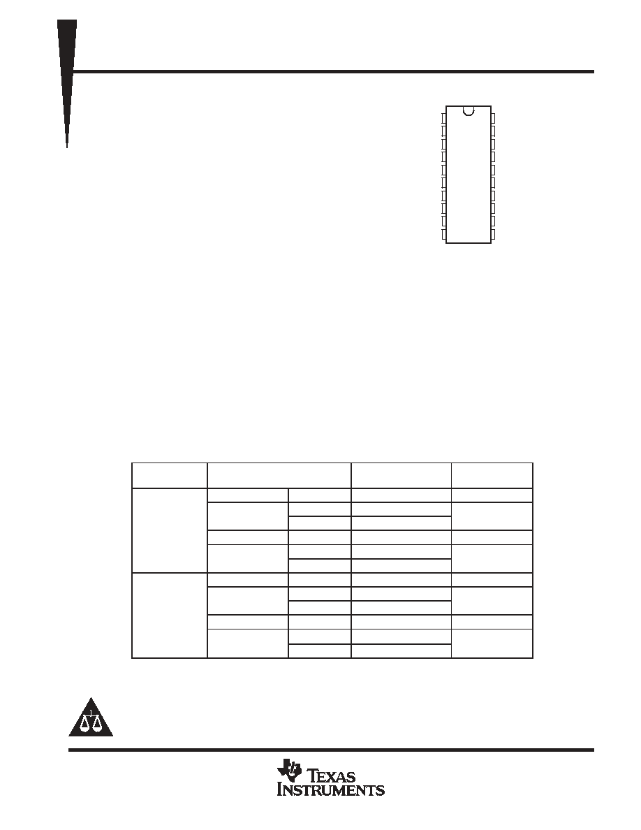
GD65232, GD75232 . . . DB, DW, N, OR PW PACKAGE
(TOP VIEW)
Please be aware that an important notice concerning availability, standard warranty, and use in critical applications of
Texas Instruments semiconductor products and disclaimers thereto appears at the end of this data sheet.
IBM is a trademark of International Business Machines Corporation.
GD65232, GD75232
MULTIPLE RS 232 DRIVERS AND RECEIVERS
SLLS206J - MAY 1995 - REVISED NOVEMBER 2004
2
POST OFFICE BOX 655303
∑
DALLAS, TEXAS 75265
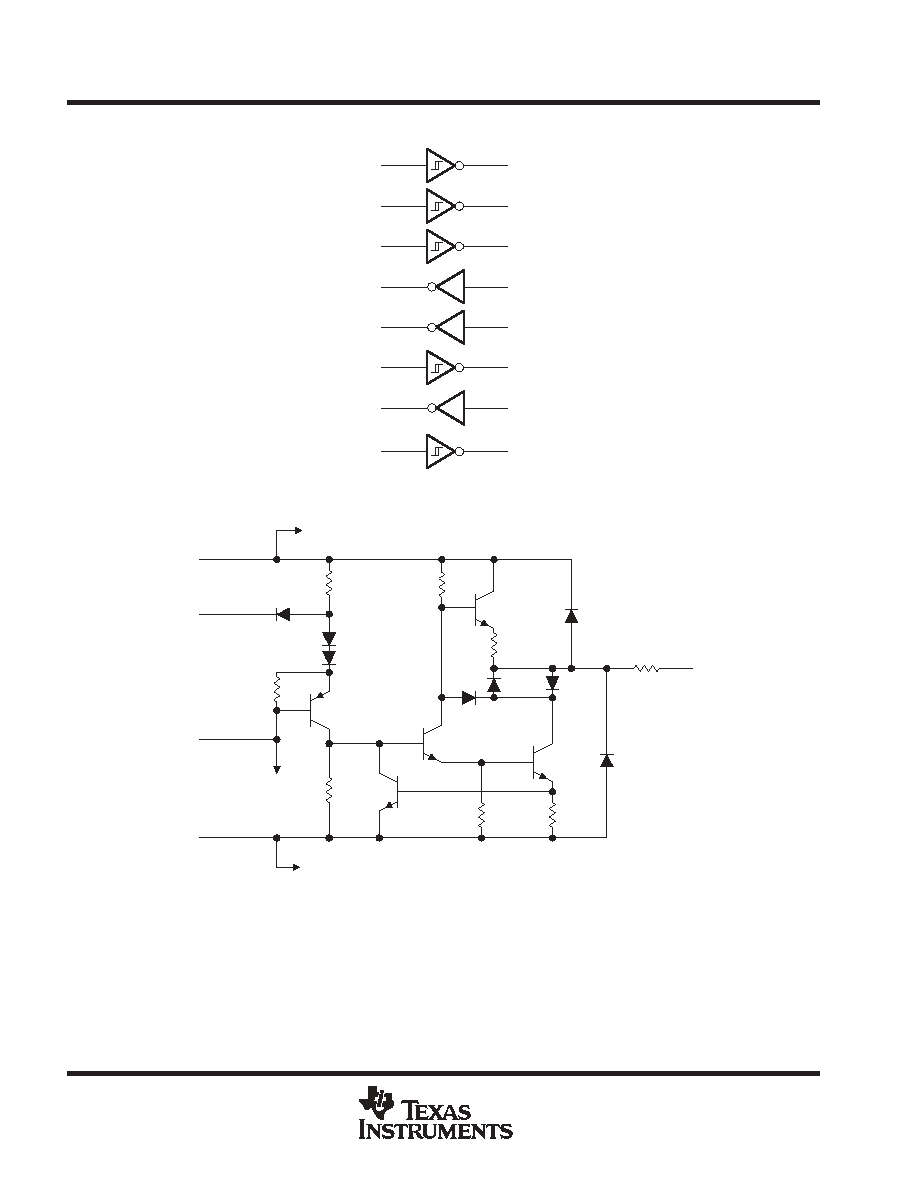
logic diagram (positive logic)
2
3
4
5
6
7
8
9
19
18
17
16
15
14
13
12
RA1
RA2
RA3
DY1
DY2
RA4
DY3
RA5
RY1
RY2
RY3
DA1
DA2
RY4
DA3
RY5
schematic (each driver)
Output
DYx
320
68.5
3.3 k
10.4 k
To Other Drivers
VSS
To Other
Drivers
GND
4.2 k
Input
DAx
VDD
75.8
9.4 k
11.6 k
To Other Drivers
Resistor values shown are nominal.
GD65232, GD75232
MULTIPLE RS 232 DRIVERS AND RECEIVERS
SLLS206J - MAY 1995 - REVISED NOVEMBER 2004
3
POST OFFICE BOX 655303
∑
DALLAS, TEXAS 75265
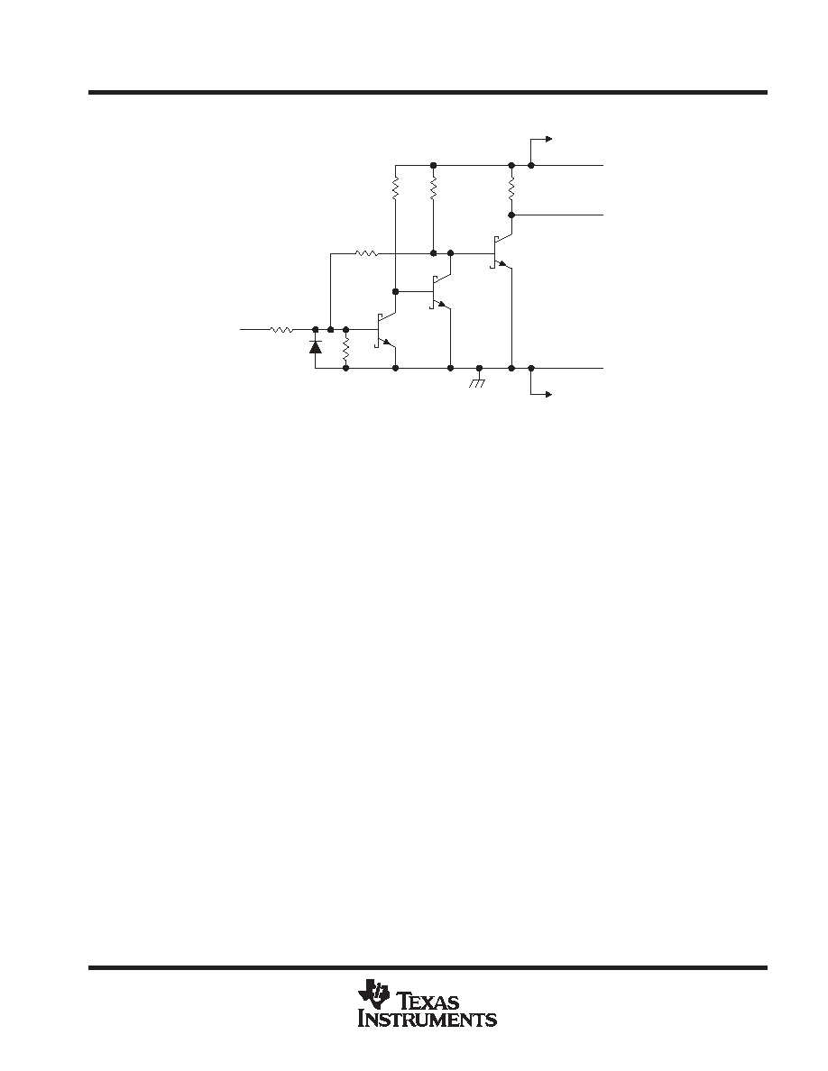
schematic (each receiver)
Input
RAx
10 k
3.8 k
9 k
5 k
1.66 k
GND
Output
RYx
VCC
To Other Receivers
Resistor values shown are nominal.
2 k
To Other Receivers
absolute maximum ratings over operating free-air temperature range (unless otherwise noted)
Supply voltage (see Note 1): V
CC
10
V
. . . . . . . . . . . . . . . . . . . . . . . . . . . . . . . . . . . . . . . . . . . . . . . . . . . . . . . . . . .
V
DD
15
V
. . . . . . . . . . . . . . . . . . . . . . . . . . . . . . . . . . . . . . . . . . . . . . . . . . . . . . . . . . .
V
SS
-15
V
. . . . . . . . . . . . . . . . . . . . . . . . . . . . . . . . . . . . . . . . . . . . . . . . . . . . . . . . . . .
Input voltage range, V
I
: Driver
-15 V to 7 V
. . . . . . . . . . . . . . . . . . . . . . . . . . . . . . . . . . . . . . . . . . . . . . . . . . . . . . . .
Receiver
-30 V to 30 V
. . . . . . . . . . . . . . . . . . . . . . . . . . . . . . . . . . . . . . . . . . . . . . . . . . .
Driver output voltage range, V
O
-15 V to 15 V
. . . . . . . . . . . . . . . . . . . . . . . . . . . . . . . . . . . . . . . . . . . . . . . . . . . . . .
Receiver low-level output current, I
OL
20
mA
. . . . . . . . . . . . . . . . . . . . . . . . . . . . . . . . . . . . . . . . . . . . . . . . . . . . . .
Package thermal impedance,
JA
(see Notes 2 and 3): DB package
70
∞
C/W
. . . . . . . . . . . . . . . . . . . . . . . . . . .
DW package
58
∞
C/W
. . . . . . . . . . . . . . . . . . . . . . . . . .
N package
69
∞
C/W
. . . . . . . . . . . . . . . . . . . . . . . . . . . .
PW package
83
∞
C/W
. . . . . . . . . . . . . . . . . . . . . . . . . .
Operating virtual junction temperature, T
J
150
∞
C
. . . . . . . . . . . . . . . . . . . . . . . . . . . . . . . . . . . . . . . . . . . . . . . . . . .
Storage temperature range, T
stg
-65
∞
C to 150
∞
C
. . . . . . . . . . . . . . . . . . . . . . . . . . . . . . . . . . . . . . . . . . . . . . . . . .
Stresses beyond those listed under "absolute maximum ratings" may cause permanent damage to the device. These are stress ratings only, and
functional operation of the device at these or any other conditions beyond those indicated under "recommended operating conditions" is not
implied. Exposure to absolute-maximum-rated conditions for extended periods may affect device reliability.
NOTES:
1. All voltages are with respect to the network ground terminal.
2. Maximum power dissipation is a function of TJ(max),
q
JA, and TA. The maximum allowable power dissipation at any allowable
ambient temperature is PD = (TJ(max) - TA)/
q
JA. Operating at the absolute maximum TJ of 150
∞
C can affect reliability.
3. The package thermal impedance is calculated in accordance with JESD 51-7.

GD65232, GD75232
MULTIPLE RS 232 DRIVERS AND RECEIVERS
SLLS206J - MAY 1995 - REVISED NOVEMBER 2004
4
POST OFFICE BOX 655303
∑
DALLAS, TEXAS 75265
recommended operating conditions
MIN
NOM
MAX
UNIT
VDD
Supply voltage (see Note 4)
7.5
9
15
V
VSS
Supply voltage (see Note 4)
-7.5
-9
-15
V
VCC
Supply voltage (see Note 4)
4.5
5
5.5
V
VIH
High-level input voltage (driver only)
1.9
V
VIL
Low-level input voltage (driver only)
0.8
V
IOH
High-level output current
Driver
-6
mA
IOH
High-level output current
Receiver
-0.5
mA
IOL
Low-level output current
Driver
6
mA
IOL
Low-level output current
Receiver
16
mA
TA
Operating free-air temperature
GD65232
-40
85
∞
C
TA
Operating free-air temperature
GD75232
0
70
∞
C
NOTE 4: When powering up the GD65232 and GD75232, the following sequence should be used:
1. VSS
2. VDD
3. VCC
4. I/Os
Applying VCC before VDD may allow large currents to flow, causing damage to the device. When powering down the GD65232 and
GD75232, the reverse sequence should be used.
supply currents over recommended operating free-air temperature range
PARAMETER
TEST CONDITIONS
MIN
MAX
UNIT
VDD = 9 V,
VSS = -9 V
15
All inputs at 1.9 V,
No load
VDD = 12 V,
VSS = -12 V
19
IDD
Supply current from VDD
All inputs at 1.9 V,
No load
VDD = 15 V,
VSS = -15 V
25
mA
IDD
Supply current from VDD
VDD = 9 V,
VSS = -9 V
4.5
mA
All inputs at 0.8 V,
No load
VDD = 12 V,
VSS = -12 V
5.5
All inputs at 0.8 V,
No load
VDD = 15 V,
VSS = -15 V
9
VDD = 9 V,
VSS = -9 V
-15
All inputs at 1.9 V,
No load
VDD = 12 V,
VSS = -12 V
-19
ISS
Supply current from VSS
All inputs at 1.9 V,
No load
VDD = 15 V,
VSS = -15 V
-25
mA
ISS
Supply current from VSS
VDD = 9 V,
VSS = -9 V
-3.2
mA
All inputs at 0.8 V,
No load
VDD = 12 V,
VSS = -12 V
-3.2
All inputs at 0.8 V,
No load
VDD = 15 V,
VSS = -15 V
-3.2
ICC
Supply current from VCC
All inputs at 5 V,
No load,
VCC = 5 V
GD65232
38
mA
ICC
Supply current from VCC
All inputs at 5 V,
No load,
VCC = 5 V
GD75232
30
mA
GD65232, GD75232
MULTIPLE RS 232 DRIVERS AND RECEIVERS
SLLS206J - MAY 1995 - REVISED NOVEMBER 2004
5
POST OFFICE BOX 655303
∑
DALLAS, TEXAS 75265
DRIVER SECTION
electrical characteristics over recommended operating free-air temperature range, V
DD
= 9 V,
V
SS
= -9 V, V
CC
= 5 V (unless otherwise noted)
PARAMETER
TEST CONDITIONS
MIN
TYP
MAX
UNIT
VOH
High-level output voltage
VIL = 0.8 V,
RL = 3 k
,
See Figure 1
6
7.5
V
VOL
Low-level output voltage (see Note 5)
VIH = 1.9 V,
RL = 3 k
,
See Figure 1
-7.5
-6
V
IIH
High-level input current
VI = 5 V,
See Figure 2
10
µ
A
IIL
Low-level input current
VI = 0,
See Figure 2
-1.6
mA
IOS(H)
High-level short-circuit output current
(see Note 6)
VIL = 0.8 V,
VO = 0,
See Figure 1
-4.5
-12
-19.5
mA
IOS(L)
Low-level short-circuit output current
VIH = 2 V,
VO = 0,
See Figure 1
4.5
12
19.5
mA
ro
Output resistance (see Note 7)
VCC = VDD = VSS = 0,
VO = -2 V to 2 V
300
NOTES:
5. The algebraic convention, where the more positive (less negative) limit is designated as maximum, is used in this data sheet for logic
levels only (e.g., if -10 V is maximum, the typical value is a more negative voltage).
6. Output short-circuit conditions must maintain the total power dissipation below absolute maximum ratings.
7. Test conditions are those specified by TIA/EIA-232-F and as listed above.
switching characteristics, V
CC
= 5 V, V
DD
= 12 V, V
SS
= -12 V, T
A
= 25
∞
C
PARAMETER
TEST CONDITIONS
MIN
TYP
MAX
UNIT
tPLH
Propagation delay time,
low- to high-level output
RL = 3 k
to 7 k
,
CL = 15 pF,
See Figure 3
315
500
ns
tPHL
Propagation delay time,
high- to low-level output
RL = 3 k
to 7 k
,
CL = 15 pF,
See Figure 3
75
175
ns
tTLH
Transition time,
RL = 3 k
to 7 k
CL = 15 pF,
See Figure 3
60
100
ns
tTLH
Transition time,
low- to high-level output
RL = 3 k
to 7 k
CL = 2500 pF,
See Figure 3 and Note 8
1.7
2.5
µ
s
tTHL
Transition time,
RL = 3 k
to 7 k
CL = 15 pF,
See Figure 3
40
75
ns
tTHL
Transition time,
high- to low-level output
RL = 3 k
to 7 k
CL = 2500 pF,
See Figure 3 and Note 8
1.5
2.5
µ
s
NOTE 8: Measured between
±
3-V and
±
3-V points of the output waveform (TIA/EIA-232-F conditions); all unused inputs are tied either high
or low.