 | –≠–ª–µ–∫—Ç—Ä–æ–Ω–Ω—ã–π –∫–æ–º–ø–æ–Ω–µ–Ω—Ç: LMV358 | –°–∫–∞—á–∞—Ç—å:  PDF PDF  ZIP ZIP |

LMV321 SINGLE, LMV358 DUAL, LMV324 QUAD
LOW-VOLTAGE RAIL-TO-RAIL OUTPUT OPERATIONAL AMPLIFIERS
SLOS263C ≠ AUGUST 1999 ≠ REVISED MARCH 2000
1
POST OFFICE BOX 655303
∑
DALLAS, TEXAS 75265
D
2.7-V and 5-V Performance
D
No Crossover Distortion
D
Low Supply Current:
LMV321 . . . 130
µ
A Typ
LMV358 . . . 210
µ
A Typ
LMV324 . . . 410
µ
A Typ
D
Rail-to-Rail Output Swing
D
Package Options Include Plastic
Small-Outline (D), Small-Outline Transistor
(SOT-23 DBV, SC-70 DCK), and Thin Shrink
Small-Outline (PW) Packages
description
The LMV324 and LMV358 are low-voltage (2.7 V
to 5.5 V) versions of the dual and quad operational
amplifiers, LM324 and LM358, that operate from
5 V to 30 V. The LMV321 is the single-amplifier
version.
The LMV321, LMV324, and LMV358 are the most
cost-effective solutions for applications where
low-voltage operation, space saving, and low
price are needed. They offer specifications that
meet or exceed those of the familiar LM358 and
LM324 devices. These devices have rail-to-rail
output-swing capability, and the input
common-mode voltage range includes ground.
They all exhibit excellent speed-to-power ratios,
achieving 1MHz of bandwidth at 1-V/
µ
s slew rate
with low supply current.
The LMV321 is available in the ultra-small DCK package, which is approximately one-half the size of the DBV
package. This package saves space on printed circuit boards and enables the design of small portable
electronic devices. It also allows the designer to place the device closer to the signal source to reduce noise
pickup and increase signal integrity.
The LMV321I, LMV324I, and LMV358I devices are characterized for operation from ≠40
∞
C to 85
∞
C.
symbol (each amplifier)
+
≠
IN ≠
IN +
OUT
Copyright
©
2000, Texas Instruments Incorporated
PRODUCTION DATA information is current as of publication date.
Products conform to specifications per the terms of Texas Instruments
standard warranty. Production processing does not necessarily include
testing of all parameters.
1
2
3
4
5
6
7
14
13
12
11
10
9
8
1OUT
1IN≠
1IN+
V
CC+
2IN+
2IN≠
2OUT
4OUT
4IN≠
4IN+
GND
3IN+
3IN≠
3OUT
LMV324 . . . D OR PW PACKAGE
(TOP VIEW)
LMV358 . . . D OR PW PACKAGE
(TOP VIEW)
1
2
3
4
8
7
6
5
1OUT
1IN≠
1IN+
GND
V
CC+
2OUT
2IN≠
2IN+
LMV321 . . . DBV OR DCK PACKAGE
(TOP VIEW)
V
CC+
OUT
1
2
3
5
4
1IN+
GND
IN≠

LMV321 SINGLE, LMV358 DUAL, LMV324 QUAD
LOW-VOLTAGE RAIL-TO-RAIL OUTPUT OPERATIONAL AMPLIFIERS
SLOS263C ≠ AUGUST 1999 ≠ REVISED MARCH 2000
2
POST OFFICE BOX 655303
∑
DALLAS, TEXAS 75265
AVAILABLE OPTIONS
TA
PACKAGE
PACKAGED DEVICES
TA
TYPE
SINGLE
DUAL
QUADRUPLE
5-pin SOT
LMV321IDCKR
LMV321IDBVR
--
--
--
--
≠40
∞
C to 85
∞
C
8-pin SOIC
8-pin TSSOP
--
--
LMV358ID
LMV358IPWR
--
--
14-pin SOIC
14-pin TSSOP
--
--
--
LMV324ID
LMV324IPWR
The D package is available taped and reeled. Add the suffix R to the device type (e.g.,
LMV324DR). The DCK, DBV, and PW packages are only available left-end taped and reeled.
absolute maximum ratings over operating free-air temperature range (unless otherwise noted)
Supply voltage, V
CC
(see Note 1)
5.5 V
. . . . . . . . . . . . . . . . . . . . . . . . . . . . . . . . . . . . . . . . . . . . . . . . . . . . . . . . . . .
Differential input voltage, V
ID
(see Note 2)
±
5.5 V
. . . . . . . . . . . . . . . . . . . . . . . . . . . . . . . . . . . . . . . . . . . . . . . . . .
Input voltage, V
I
(either input)
0 to 5.5 V
. . . . . . . . . . . . . . . . . . . . . . . . . . . . . . . . . . . . . . . . . . . . . . . . . . . . . . . . . .
Duration of output short circuit (one amplifier) to ground at (or below) T
A
=
25
∞
C,
V
CC
5.5 V (see Note 3)
Unlimited
. . . . . . . . . . . . . . . . . . . . . . . . . . . . . . . . . . . . . . . . . . . . . . . . . . . . . . . . . . . . .
Operating virtual junction temperature
150
∞
C
. . . . . . . . . . . . . . . . . . . . . . . . . . . . . . . . . . . . . . . . . . . . . . . . . . . . . .
Package thermal impedance,
JA
(see Notes 4 and 5): D (8-pin) package
197
∞
C/W
. . . . . . . . . . . . . . . . . . . . .
D (14-pin) package
127
∞
C/W
. . . . . . . . . . . . . . . . . . .
DBV package
347
∞
C/W
. . . . . . . . . . . . . . . . . . . . . . . .
DCK package
389
∞
C/W
. . . . . . . . . . . . . . . . . . . . . . . .
PW (8-pin) package
243
∞
C/W
. . . . . . . . . . . . . . . . . . .
PW (14-pin) package
170
∞
C/W
. . . . . . . . . . . . . . . . . .
Lead temperature 1,6 mm (1/16 inch) from case for 10 seconds: D or PW package
260
∞
C
. . . . . . . . . . . . . .
DBV or DCK package
TBD
. . . . . . . . . . . . .
Storage temperature range, T
stg
≠65 to 150
∞
C
. . . . . . . . . . . . . . . . . . . . . . . . . . . . . . . . . . . . . . . . . . . . . . . . . . . . .
Stresses beyond those listed under "absolute maximum ratings" may cause permanent damage to the device. These are stress ratings only, and
functional operation of the device at these or any other conditions beyond those indicated under "recommended operating conditions" is not
implied. Exposure to absolute-maximum-rated conditions for extended periods may affect device reliability.
NOTES:
1. All voltage values (except differential voltages and VCC specified for the measurement of IOS) are with respect to the network GND.
2. Differential voltages are at IN+ with respect to IN≠.
3. Short circuits from outputs to VCC can cause excessive heating and eventual destruction.
4. Maximum power dissipation is a function of TJ(max),
JA, and TA. The maximum allowable power dissipation at any allowable
ambient temperature is PD = (TJ(max) ≠ TA)/
JA. Selecting the maximum of 150
∞
C can impact reliability.
5. The package thermal impedance is calculated in accordance with JESD 51.
recommended operating conditions
MIN
MAX
UNIT
VCC
Supply voltage (single-supply operation)
2.7
5.5
V
TA
Operating free-air temperature
≠40
85
∞
C

LMV321 SINGLE, LMV358 DUAL, LMV324 QUAD
LOW-VOLTAGE RAIL-TO-RAIL OUTPUT OPERATIONAL AMPLIFIERS
SLOS263C ≠ AUGUST 1999 ≠ REVISED MARCH 2000
3
POST OFFICE BOX 655303
∑
DALLAS, TEXAS 75265
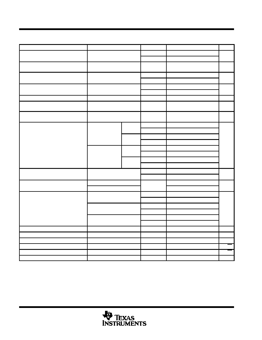
electrical characteristics at T
A
= 25
∞
C and V
CC+
= 2.7 V (unless otherwise noted)
PARAMETER
TEST CONDITIONS
MIN
TYP
MAX
UNIT
VIO
Input offset voltage
1.7
7
mV
a
V
IO
Average temperature coefficient
of input offset voltage
5
m
V/
∞
C
IIB
Input bias current
11
250
nA
IIO
Input offset current
5
50
nA
CMRR
Common-mode rejection ratio
VCM = 0 to 1.7 V
50
63
dB
kSVR
Supply-voltage rejection ratio
VCC = 2.7 V to 5 V,
VO = 1 V
50
60
dB
VICR
Common-mode input voltage range
CMRR
w
50 dB
0 to 1.7
≠0.2 to 1.9
V
Output swing
RL = 10 k
to 1 35 V
High level
VCC≠100
VCC≠10
mV
Output swing
RL = 10 k
to 1.35 V
Low level
60
180
mV
LMV321I
80
170
ICC
Supply current
LMV358I (both amplifiers)
140
340
m
A
LMV324I (all four amplifiers)
260
680
B1
Unity-gain bandwidth
CL = 200 pF
1
MHz
F
m
Phase margin
60
deg
Gm
Gain margin
10
dB
Vn
Equivalent input noise voltage
f = 1 kHz
46
nV/
Hz
In
Equivalent input noise current
f = 1 kHz
0.17
pA/
Hz
LMV321 SINGLE, LMV358 DUAL, LMV324 QUAD
LOW-VOLTAGE RAIL-TO-RAIL OUTPUT OPERATIONAL AMPLIFIERS
SLOS263C ≠ AUGUST 1999 ≠ REVISED MARCH 2000
4
POST OFFICE BOX 655303
∑
DALLAS, TEXAS 75265
electrical characteristics at specified free-air temperature range, V
CC+
= 5 V (unless otherwise
noted)
PARAMETER
TEST CONDITIONS
TA
MIN
TYP
MAX
UNIT
VIO
Input offset voltage
25
∞
C
1.7
7
mV
VIO
Input offset voltage
≠40
∞
C to 85
∞
C
9
mV
a
V
IO
Average temperature coefficient
of input offset voltage
25
∞
C
5
m
V/
∞
C
IIB
Input bias current
25
∞
C
15
250
nA
IIB
Input bias current
≠40
∞
C to 85
∞
C
500
nA
IIO
Input offset current
25
∞
C
5
50
nA
IIO
Input offset current
≠40
∞
C to 85
∞
C
150
nA
CMRR
Common-mode rejection ratio
VCM = 0 to 4 V
25
∞
C
50
65
dB
kSVR
Supply-voltage rejection ratio
VCC= 2.7 V to 5 V, VO = 1 V,
VCM = 1 V
25
∞
C
50
60
dB
VICR
Common-mode
CMMR
w
50 dB
25
∞
C
0 to 4
0 2 to 4 2
V
VICR
input voltage range
CMMR
w
50 dB
25
∞
C
0 to 4
≠0.2 to 4.2
V
High level
25
∞
C
VCC≠300
VCC≠40
RL = 2 k
to 2 5 V
High level
≠40
∞
C to 85
∞
C
VCC≠400
RL = 2 k
to 2.5 V
Low level
25
∞
C
120
300
Output swing
Low level
≠40
∞
C to 85
∞
C
400
mV
Output swing
High level
25
∞
C
VCC≠100
VCC≠10
mV
RL = 10 k
to 2 5 V
High level
≠40
∞
C to 85
∞
C
VCC≠200
RL = 10 k
to 2.5 V
Low level
25
∞
C
65
180
Low level
≠40
∞
C to 85
∞
C
280
AVD
Large-signal differential
RL = 2 k
25
∞
C
15
100
V/mV
AVD
g
g
voltage gain
RL = 2 k
≠40
∞
C to 85
∞
C
10
V/mV
IOS
Output short circuit current
Sourcing, VO = 0 V
25
∞
C
5
60
mA
IOS
Output short-circuit current
Sinking, VO = 5 V
25
∞
C
10
160
mA
LMV321I
25
∞
C
130
250
LMV321I
≠40
∞
C to 85
∞
C
350
ICC
Supply current
LMV358I (both amplifiers)
25
∞
C
210
440
m
A
ICC
Supply current
LMV358I (both amplifiers)
≠40
∞
C to 85
∞
C
615
m
A
LMV324I (all four amplifiers)
25
∞
C
410
830
LMV324I (all four amplifiers)
≠40
∞
C to 85
∞
C
1160
B1
Unity-gain bandwidth
CL = 200 pF
25
∞
C
1
MHz
f
m
Phase margin
25
∞
C
60
deg
Gm
Gain margin
25
∞
C
10
dB
Vn
Equivalent input noise voltage
f = 1 kHz
25
∞
C
39
nV/
Hz
In
Equivalent input noise current
f = 1 kHz
25
∞
C
0.21
pA/
Hz
SR
Slew rate
25
∞
C
1
V/
m
s

IMPORTANT NOTICE
Texas Instruments and its subsidiaries (TI) reserve the right to make changes to their products or to discontinue
any product or service without notice, and advise customers to obtain the latest version of relevant information
to verify, before placing orders, that information being relied on is current and complete. All products are sold
subject to the terms and conditions of sale supplied at the time of order acknowledgement, including those
pertaining to warranty, patent infringement, and limitation of liability.
TI warrants performance of its semiconductor products to the specifications applicable at the time of sale in
accordance with TI's standard warranty. Testing and other quality control techniques are utilized to the extent
TI deems necessary to support this warranty. Specific testing of all parameters of each device is not necessarily
performed, except those mandated by government requirements.
CERTAIN APPLICATIONS USING SEMICONDUCTOR PRODUCTS MAY INVOLVE POTENTIAL RISKS OF
DEATH, PERSONAL INJURY, OR SEVERE PROPERTY OR ENVIRONMENTAL DAMAGE ("CRITICAL
APPLICATIONS"). TI SEMICONDUCTOR PRODUCTS ARE NOT DESIGNED, AUTHORIZED, OR
WARRANTED TO BE SUITABLE FOR USE IN LIFE-SUPPORT DEVICES OR SYSTEMS OR OTHER
CRITICAL APPLICATIONS. INCLUSION OF TI PRODUCTS IN SUCH APPLICATIONS IS UNDERSTOOD TO
BE FULLY AT THE CUSTOMER'S RISK.
In order to minimize risks associated with the customer's applications, adequate design and operating
safeguards must be provided by the customer to minimize inherent or procedural hazards.
TI assumes no liability for applications assistance or customer product design. TI does not warrant or represent
that any license, either express or implied, is granted under any patent right, copyright, mask work right, or other
intellectual property right of TI covering or relating to any combination, machine, or process in which such
semiconductor products or services might be or are used. TI's publication of information regarding any third
party's products or services does not constitute TI's approval, warranty or endorsement thereof.
Copyright
©
2000, Texas Instruments Incorporated