Document Outline
- features
- description
- pin designation
- functional block diagram
- MSP430F42x Terminal Functions
- short-form description
- CPU
- instruction set
- operating modes
- interrupt vector addresses
- special function registers
- interrupt enable 1 and 2
- interrupt flag register 1 and 2
- module enable registers 1 and 2
- memory organization
- bootstrap loader (BSL)
- flash memory
- peripherals
- oscillator and system clock
- brownout, supply voltage supervisor
- digital I/O
- Basic Timer1
- LCD drive
- WDT+ watchdog timer
- timer_A3
- USART0
- hardware multiplier
- SD16
- peripheral file map
- absolute maximum ratingsÅ
- recommended operating conditions
- electrical characteristics over recommended operating free-air temperature (unless otherwise noted)
- supply current into AVCC + DVCC excluding external current, ( see Note 1)
- current consumption of active mode versus system frequency, F version
- current consumption of active mode versus supply voltage, F version
- Schmitt-trigger inputs - Ports P1 and P2; RST\/NMI; JTAG: TCK, TMS, TDI/TCLK, TDO/TDI
- inputs Px.x, TAx
- leakage current (see Note 1)
- outputs - Ports P1 and P2
- output frequency
- wake-up LPM3
- RAM (see Note 1)
- LCD
- USART0 (see Note 1)
- POR brownout, reset (see Notes 1 and 2)
- SVS (supply voltage supervisor/monitor) (see Note 1)
- DCO
- crystal oscillator, LFXT1 oscillator (see Notes 1 and 2)
- SD16, power supply and recommended operating conditions
- SD16, analog input range (see Note 1)
- SD16, analog performance ( fSD16 = 1MHz, SD16OSRx = 256, SD16REFON = 1)
- SD16, built-in temperature sensor
- SD16, built-in voltage reference
- SD16, built-in reference output buffer
- SD16, external reference input
- Flash Memory
- JTAG Interface
- JTAG Fuse (see Note 1)
- APPLICATION INFORMATION
- input/output schematic
- Port P1, P1.0 to P1.1, input/output with Schmitt-trigger
- Port P1, P1.2 to P1.7, input/output with Schmitt-trigger
- port P2, P2.0 to P2.1, input/output with Schmitt-trigger
- port P2, P2.2 to P2.5, input/output with Schmitt-trigger
- Port P2, unbonded GPIOs P2.6 and P2.7
- JTAG pins TMS, TCK, TDI, TDO/TDI, input/output with Schmitt-trigger or output
- JTAG fuse check mode
- IMPORTANT NOTICE

MSP430F42x
MIXED SIGNAL MICROCONTROLLER
SLAS421 - APRIL 2004
1
POST OFFICE BOX 655303
∑
DALLAS, TEXAS 75265
D
Low Supply-Voltage Range, 1.8 V . . . 3.6 V
D
Ultralow-Power Consumption:
- Active Mode: 400
µ
A at 1 MHz, 3.0 V
- Standby Mode: 1.6
µ
A
- Off Mode (RAM Retention): 0.1
µ
A
D
Five Power-Saving Modes
D
Wake-Up From Standby Mode in less
than 6
µ
s
D
Frequency-Locked Loop, FLL+
D
16-Bit RISC Architecture, 125-ns
Instruction Cycle Time
D
Three Independent 16-bit Sigma-Delta A/D
Converters with Differential PGA Inputs
D
16-Bit Timer_A With Three
Capture/Compare Registers
D
Integrated LCD Driver for 128 Segments
D
Serial Communication Interface (USART),
Asynchronous UART or Synchronous SPI
selectable by software
D
Brownout Detector
D
Supply Voltage Supervisor/Monitor With
Programmable Level Detection
D
Serial Onboard Programming,
No External Programming Voltage Needed
Programmable Code Protection by Security
Fuse
D
Bootstrap Loader in Flash Devices
D
Family Members Include:
- MSP430F423:
8KB + 256B Flash Memory,
256B RAM
- MSP430F425:
16KB + 256B Flash Memory,
512B RAM
- MSP430F427:
32KB + 256B Flash Memory,
1KB RAM
D
Available in 64-Pin Quad Flat Pack (QFP)
D
For Complete Module Descriptions, Refer
to the MSP430x4xx Family User's Guide,
Literature Number SLAU056
description
The Texas Instruments MSP430 family of ultralow power microcontrollers consist of several devices featuring
different sets of peripherals targeted for various applications. The architecture, combined with five low power
modes is optimized to achieve extended battery life in portable measurement applications. The device features
a powerful 16-bit RISC CPU, 16-bit registers, and constant generators that attribute to maximum code efficiency.
The digitally controlled oscillator (DCO) allows wake-up from low-power modes to active mode in less than 6
µ
s.
The MSP430F42x series are microcontroller configurations with three independent 16-bit sigma-delta A/D
converters, each with an integrated differential programmable gain amplifier input stage. Also included is a
built-in 16-bit timer, 128 LCD segment drive capability, hardware multiplier and 14 I/O pins.
Typical applications include high resolution applications such as handheld metering equipment, weigh scales
and energy meters.
AVAILABLE OPTIONS
PACKAGED DEVICES
TA
PLASTIC 64-PIN QFP
(PM)
-40
∞
C to 85
∞
C
MSP430F423IPM
MSP430F425IPM
MSP430F427IPM
Copyright
2004 Texas Instruments Incorporated
PRODUCTION DATA information is current as of publication date.
Products conform to specifications per the terms of Texas Instruments
standard warranty. Production processing does not necessarily include
testing of all parameters.
Please be aware that an important notice concerning availability, standard warranty, and use in critical applications of
Texas Instruments semiconductor products and disclaimers thereto appears at the end of this data sheet.

MSP430F42x
MIXED SIGNAL MICROCONTROLLER
SLAS421 - APRIL 2004
2
POST OFFICE BOX 655303
∑
DALLAS, TEXAS 75265
pin designation
{
17 18 19 20 21 22 23 24 25 26 27 28 29 30 31 32
64 63 62 61 60 59 58 57 56 55 54 53 52 51 50 49
P1.5/TACLK/ACLK/S28
P2.3/SVSIN
P2.4/UTXD0
P2.5/URXD0
RST/NMI
TCK
TMS
TDI/TCLK
TDO/TDI
P1.0/T
A0
P1.1/T
A0/MCLK
P1.2/T
A1/S31
P1.3/SVSOUT/S3
0
P1.4/S29
S5
S6
S7
S8
S9
S10
S1
1
S12
S13
S14
S15
S16
S17
S
18
S19
S20
48
47
46
45
44
43
42
41
40
39
38
37
36
35
34
33
P1.6/SIMO0/S27
P1.7/SOMI0/S26
P2.0/TA2/S25
P2.1/UCLK0/S24
R33
R23
R13
R03
COM3
COM2
COM1
COM0
S23
S21
S22
1
2
3
4
5
6
7
8
9
10
11
12
13
14
15
16
A0.0+
A0.0-
A1.0+
A1.0-
A2.0+
A2.0-
XIN
XOUT
P2.2/STE0
S0
S1
S2
S4
S3
MSP430F42x
V
REF
AV
CC
DV
CC
AV
SS
DV
SS
Open connection recommended for all unused analog inputs.
MSP430F42x
MIXED SIGNAL MICROCONTROLLER
SLAS421 - APRIL 2004
3
POST OFFICE BOX 655303
∑
DALLAS, TEXAS 75265
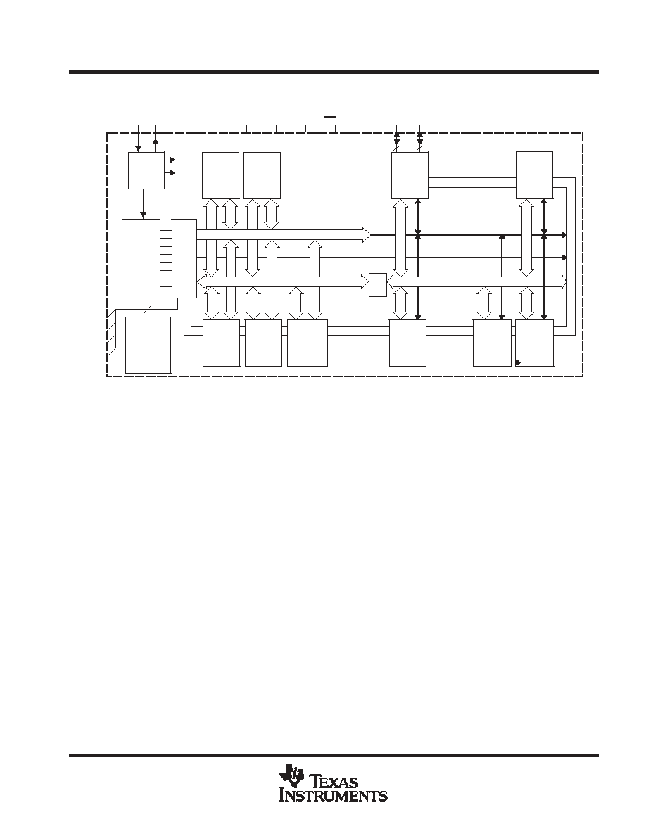
functional block diagram
Oscillator
ACLK
SMCLK
CPU
Incl. 16 Reg.
Bus
Conv
MCB
XIN
XOUT
P2
TMS
TCK
MDB, 16 Bit
MAB, 16 Bit
MCLK
4
TDI/TCLK
TDO/TDI
MAB,
4 Bit
DVCC
DVSS
AVCC
AVSS RST/NMI
P1
32KB Flash
16KB Flash
8KB Flash
1KB RAM
512B RAM
256B RAM
Watchdog
Timer
15/16-Bit
Timer_A3
3 CC Reg
Test
JTAG
Emulation
Module
I/O Port 1/2
14 I/Os,
with
Interrupt
Capability
POR/
SVS/
Brownout
Basic
Timer 1
1 Interrupt
Vector
MDB, 8 Bit
MDB, 16-Bit
MAB, 16-Bit
LCD
128
Segments
1,2,3,4 MUX
fLCD
FLL+
8
6
USART0
UART or
SPI
Function
SD16
Three 16-bit
Sigma-Delta
A/D
Converters
Hardware
Multiplier
MPY, MPYS
MAC,MACS

MSP430F42x
MIXED SIGNAL MICROCONTROLLER
SLAS421 - APRIL 2004
4
POST OFFICE BOX 655303
∑
DALLAS, TEXAS 75265
MSP430F42x Terminal Functions
TERMINAL
PN
I/O
DESCRIPTION
NAME
NO.
I/O
DESCRIPTION
DVCC
1
Digital supply voltage, positive terminal. Supplies all digital parts.
A0.0+
2
I
Internal connection to SD16 Channel 0, input 0 +. (see Note 1)
A0.0-
3
I
Internal connection to SD16 Channel 0, input 0 -. (see Note 1)
A1.0+
4
I
Internal connection to SD16 Channel 1, input 0 +. (see Note 1)
A1.0-
5
I
Internal connection to SD16 Channel 1, input 0 -. (see Note 1)
A2.0+
6
I
Internal connection to SD16 Channel 2, input 0 +. (see Note 1)
A2.0-
7
I
Internal connection to SD16 Channel 2, input 0 -. (see Note 1)
XIN
8
I
Input port for crystal oscillator XT1. Standard or watch crystals can be connected.
XOUT
9
O
Output terminal of crystal oscillator XT1
VREF
10
I/O
Input for an external reference voltage / internal reference voltage output (can be used as mid-voltage)
P2.2/STE0
11
I/O
General-purpose digital I/O / slave transmit enable--USART0/SPI mode
S0
12
O
LCD segment output 0
S1
13
O
LCD segment output 1
S2
14
O
LCD segment output 2
S3
15
O
LCD segment output 3
S4
16
O
LCD segment output 4
S5
17
O
LCD segment output 5
S6
18
O
LCD segment output 6
S7
19
O
LCD segment output 7
S8
20
O
LCD segment output 8
S9
21
O
LCD segment output 9
S10
22
O
LCD segment output 10
S11
23
O
LCD segment output 11
S12
24
O
LCD segment output 12
S13
25
O
LCD segment output 13
S14
26
O
LCD segment output 14
S15
27
O
LCD segment output 15
S16
28
O
LCD segment output 16
S17
29
O
LCD segment output 17
S18
30
O
LCD segment output 18
S19
31
O
LCD segment output 19
S20
32
O
LCD segment output 20
S21
33
O
LCD segment output 21
S22
34
O
LCD segment output 22
S23
35
O
LCD segment output 23
COM0
36
O
Common output, COM0-3 are used for LCD backplanes.
COM1
37
O
Common output, COM0-3 are used for LCD backplanes.
COM2
38
O
Common output, COM0-3 are used for LCD backplanes.
COM3
39
O
Common output, COM0-3 are used for LCD backplanes.
R03
40
I
Input port of fourth positive (lowest) analog LCD level (V5)
NOTE 1: Open connection recommended for all unused analog inputs.

MSP430F42x
MIXED SIGNAL MICROCONTROLLER
SLAS421 - APRIL 2004
5
POST OFFICE BOX 655303
∑
DALLAS, TEXAS 75265
MSP430F42x Terminal Functions (Continued)
TERMINAL
PN
I/O
DESCRIPTION
NAME
NO.
I/O
DESCRIPTION
R13
41
I
Input port of third most positive analog LCD level (V4 or V3)
R23
42
I
Input port of second most positive analog LCD level (V2)
R33
43
O
Output port of most positive analog LCD level (V1)
P2.1/UCLK0/S24
44
I/O
General-purpose digital I/O / external clock input-USART0/UART or SPI mode, clock output--USART0/SPI
mode / LCD segment output 24 (See Note 1)
P2.0/TA2/S25
45
I/O
General-purpose digital I/O / Timer_A Capture: CCI2A input, Compare: Out2 output / LCD segment output
25 (See Note 1)
P1.7/SOMI0/S26
46
I/O
General-purpose digital I/O / slave out/master in of USART0/SPI mode / LCD segment output 26
(See Note 1)
P1.6/SIMO0/S27
47
I/O
General-purpose digital I/O / slave in/master out of USART0/SPI mode / LCD segment output 27
(See Note 1)
P1.5/TACLK/
ACLK/S28
48
I/O
General-purpose digital I/O / Timer_A and SD16 clock signal TACLK input / ACLK output (divided by 1,
2, 4, or 8) / LCD segment output 28 (See Note 1)
P1.4/S29
49
I/O
General-purpose digital I/O / LCD segment output 29 (See Note 1)
P1.3/SVSOUT/
S30
50
I/O
General-purpose digital I/O / SVS: output of SVS comparator / LCD segment output 30 (See Note 1)
P1.2/TA1/S31
51
I/O
General-purpose digital I/O / Timer_A, Capture: CCI1A, CCI1B input, Compare: Out1 output / LCD segment
output 31 (See Note 1)
P1.1/TA0/MCLK
52
I/O
General-purpose digital I/O / Timer_A, Capture: CCI0B input / MCLK output.
Note: TA0 is only an input on this pin / BSL receive
P1.0/TA0
53
I/O
General-purpose digital I/O / Timer_A, Capture: CCI0A input, Compare: Out0 output / BSL transmit
TDO/TDI
54
I/O
Test data output port. TDO/TDI data output or programming data input terminal.
TDI/TCLK
55
I
Test data input or test clock input. The device protection fuse is connected to TDI.
TMS
56
I
Test mode select. TMS is used as an input port for device programming and test.
TCK
57
I
Test clock. TCK is the clock input port for device programming and test.
RST/NMI
58
I
Reset input or nonmaskable interrupt input port
P2.5/URXD0
59
I/O
General-purpose digital I/O / receive data in--USART0/UART mode
P2.4/UTXD0
60
I/O
General-purpose digital I/O / transmit data out--USART0/UART mode
P2.3/SVSIN
61
I/O
General-purpose digital I/O / Analog input to brownout, supply voltage supervisor
AVSS
62
Analog supply voltage, negative terminal. Supplies SD16, SVS, brownout, oscillator, FLL+, and LCD
resistive divider circuitry.
DVSS
63
Digital supply voltage, negative terminal. Supplies all digital parts, except those which are supplied via
AVCC/AVSS.
AVCC
64
Analog supply voltage, positive terminal. Supplies SD16, SVS, brownout, oscillator, FLL+, and LCD
resistive divider circuitry; must not power up prior to DVCC.
NOTE 1: LCD function selected automatically when applicable LCD module control bits are set, not with PxSEL bits.