Document Outline
- features
- description
- pin designation, MSP430F42x0
- MSP430F42x0 functional block diagram
- MSP430F42x0 Terminal Functions
- short-form description
- CPU
- instruction set
- operating modes
- interrupt vector addresses
- special function registers
- interrupt enable registers 1 and 2
- interrupt flag registers 1 and 2
- module enable registers 1 and 2
- memory organization
- bootstrap loader (BSL)
- flash memory
- peripherals
- oscillator and system clock
- brownout
- digital I/O
- Basic Timer1
- LCD driver with regulated charge pump
- watchdog timer
- timer_A3
- SD16_A
- DAC12
- peripheral file map
- absolute maximum ratings over operating free-air temperature (unless otherwise noted)Å
- recommended operating conditions
- electrical characteristics over recommended operating free-air temperature (unless otherwise noted)
- supply current into AVCC + DVCC excluding external current
- Current consumption of active mode versus system frequency, F-version:
- Current consumption of active mode versus supply voltage, F-version:
- SCHMITT-trigger inputs - Ports P1, P2, P5, and P6; RST\/NMI; JTAG: TCK, TMS, TDI/TCLK, TDO/TDI
- inputs Px.x, TAx
- leakage current - Ports P1, P2, P5, and P6 (see Note 1)
- outputs - Ports P1, P2, P5, and P6
- output frequency
- wake-up LPM3
- RAM
- LCD_A
- POR/brownout reset (BOR) (see Note 1)
- typical characteristics
- electrical characteristics over recommended operating free-air temperature (unless otherwise noted)
- DCO
- crystal oscillator, LFXT1 oscillator (see Notes 1 and 2)
- SD16_A, power supply and recommended operating conditions
- SD16_A, input range
- SD16_A, performance ( fSD16 = 30kHz, SD16REFON = 1, SD16BUFx = 01)
- SD16_A, performance ( fSD16 = 1MHz, SD16OSRx = 256, SD16REFON = 1, SD16BUFx = 00)
- SD16_A, temperature sensor
- SD16_A, built-in voltage reference
- SD16_A, reference output buffer
- SD16_A, external reference input
- 12-bit DAC, supply specifications
- 12-bit DAC, linearity specifications (see Figure 12)
- 12-bit DAC, output specifications
- 12-bit DAC, reference input specifications
- 12-bit DAC, dynamic specifications; VREF,DAC12 = AVCC, DAC12IR = 1 (see Figure 16 and Figure 17)
- 12-bit DAC, dynamic specifications continued (TA = 25∞C unless otherwise noted)
- Flash Memory
- JTAG Interface
- JTAG Fuse (see Note 1)
- input/output schematics
- Port P1 pin schematic: P1.0, P1.1, input/output with Schmitt-trigger
- Port P1 (P1.0, P1.1) pin functions
- Port P1 pin schematic: P1.2, input/output with Schmitt-trigger and analog functions
- Port P1 (P1.2) pin functions
- Port P1 pin schematic: P1.3, P1.5, P1.7, input/output with Schmitt-trigger and analog functions
- Port P1 (P1.3, P1.5, P1.7) pin functions
- Port P1 pin schematic: P1.4, input/output with Schmitt-trigger and analog functions
- Port P1 (P1.4) pin functions
- Port P1 pin schematic: P1.6, input/output with Schmitt-trigger and analog functions
- Port P1 (P1.6) pin functions
- Port P2 pin schematic: P2.0 to P2.7, input/output with Schmitt-trigger, LCD and analog functions
- Port P2 (P2.0 to P2.7) pin functions
- Port P5 pin schematic: P5.0, P5.1, P5.5 to P5.7, input/output with Schmitt-trigger and LCD functions
- Port P5 (P5.0, P5.1, P5.5, P5.6) pin functions
- Port P5 (P5.7) pin functions
- Port P5 pin schematic: P5.2 to P5.4, input/output with Schmitt-trigger and LCD functions
- Port P5 (P5.2 to P5.4) pin functions
- Port P6 pin schematic: P6.0, P6.2, input/output with Schmitt-trigger and analog functions
- Port P6 (P6.0, P6.2) pin functions
- Port P6 pin schematic: P6.1, P6.3, input/output with Schmitt-trigger and analog functions
- Port P6 (P6.1, P6.3) pin functions
- Port P6 pin schematic: P6.4 to P6.7, input/output with Schmitt-trigger and analog functions
- Port P6 (P6.4 to P6.7) pin functions
- JTAG pins TMS, TCK, TDI/TCLK, TDO/TDI, input/output with Schmitt-trigger or output
- JTAG fuse check mode

MSP430F42x0
MIXED SIGNAL MICROCONTROLLER
SLAS455C - MARCH 2005 - REVISED AUGUST 2005
1
POST OFFICE BOX 655303
∑
DALLAS, TEXAS 75265
D
Low Supply-Voltage Range, 1.8 V to 3.6 V
D
Ultralow-Power Consumption:
Active Mode: 250
µ
A at 1 MHz, 2.2 V
Standby Mode: 1.1
µ
A
Off Mode (RAM Retention): 0.1
µ
A
D
Five Power Saving Modes
D
Wake-Up From Standby Mode in less
than 6
µ
s
D
16-Bit RISC Architecture,
125-ns Instruction Cycle Time
D
16-Bit Sigma-Delta A/D Converter With
Internal Reference and Five Differential
Analog Inputs
D
12-Bit D/A Converter
D
16-Bit Timer_A With Three
Capture/Compare Registers
D
Brownout Detector
D
Bootstrap Loader
D
Serial Onboard Programming,
No External Programming Voltage Needed
Programmable Code Protection by Security
Fuse
D
Integrated LCD Driver with Contrast
Control for Up to 56 Segments
D
MSP430x42x0 Family Members Include:
MSP430F4250: 16KB+256B Flash Memory
256B RAM
MSP430F4260: 24KB+256B Flash Memory
256B RAM
MSP430F4270: 32KB+256B Flash Memory
256B RAM
D
For Complete Module Descriptions, See
The MSP430x4xx Family User's Guide,
Literature Number SLAU056
D
For Additional Device Information, See The
MSP430F42x0 Device Erratasheet,
Literature Number SLAZ022
description
The Texas Instruments MSP430 family of ultralow power microcontrollers consist of several devices featuring
different sets of peripherals targeted for various applications. The architecture, combined with five low power
modes is optimized to achieve extended battery life in portable measurement applications. The device features
a powerful 16-bit RISC CPU, 16-bit registers, and constant generators that attribute to maximum code efficiency.
The digitally controlled oscillator (DCO) allows wake-up from low-power modes to active mode in less than 6
µ
s.
The MSP430F42x0 is a microcontroller configuration with a 16-bit timer, a high performance 16-bit sigma-delta
A/D converter, 12-bit D/A converter, 32 I/O pins, and a liquid crystal display driver.
Typical applications for this device include analog and digital sensor systems, digital motor control, remote
controls, thermostats, digital timers, hand-held meters, etc.
AVAILABLE OPTIONS
PACKAGED DEVICES
TA
PLASTIC 48-PIN SSOP
(DL)
PLASTIC 48-PIN QFN
(RGZ)
MSP430F4250IDL
MSP430F4250IRGZ
-40
∞
C to 85
∞
C
MSP430F4260IDL
MSP430F4260IRGZ
-40 C to 85 C
MSP430F4270IDL
MSP430F4270IRGZ
This integrated circuit can be damaged by ESD. Texas Instruments recommends that all integrated circuits be handled with
appropriate precautions. Failure to observe proper handling and installation procedures can cause damage. ESD damage can range
from subtle performance degradation to complete device failure. Precision integrated circuits may be more susceptible to damage
because very small parametric changes could cause the device not to meet its published specifications. These devices have limited
built-in ESD protection.
PRODUCTION DATA information is current as of publication date.
Products conform to specifications per the terms of Texas Instruments
standard warranty. Production processing does not necessarily include
testing of all parameters.
Copyright
2005, Texas Instruments Incorporated
Please be aware that an important notice concerning availability, standard warranty, and use in critical applications of
Texas Instruments semiconductor products and disclaimers thereto appears at the end of this data sheet.

MSP430F42x0
MIXED SIGNAL MICROCONTROLLER
SLAS455C - MARCH 2005 - REVISED AUGUST 2005
2
POST OFFICE BOX 655303
∑
DALLAS, TEXAS 75265
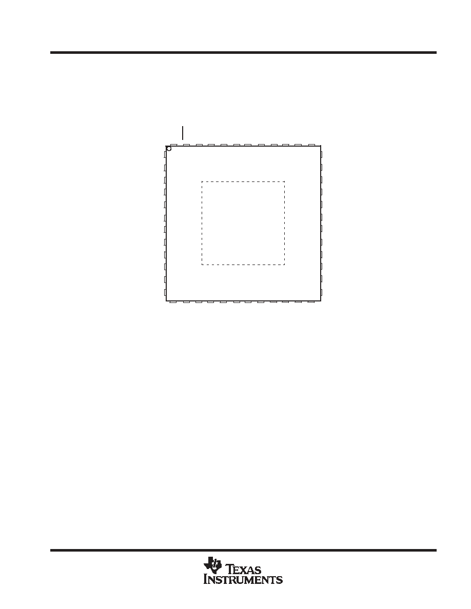
pin designation, MSP430F42x0
P5.4/COM3
P5.3/COM2
P5.2/COM1
COM0
P2.0/S13
P2.1/S12
P2.2/S11
P2.3/S10
P2.4/S9
P2.5/S8
P2.6/S7
P2.7/S6
S5
P5.7/S4
P5.6/S3
P5.5/S2
P5.0/S1
P5.1/S0
LCDCAP/R23
LCDREF/R13
P1.0/TA0
P1.1/TA0/MCLK
P1.2/TA1/A4-
P1.3/TA2/A4+
TDO/TDI
TDI/TCLK
TMS
TCK
RST/NMI
DV
CC
DV
SS
XIN
XOUT
AV
SS
AV
CC
V
REF
P6.0/A0+
P6.1/A0-
P6.2/A1+
P6.3/A1-
P6.4
P6.5
P6.6
P6.7
P1.7/A2+
P1.6/A2-
P1.5/TACLK/ACLK/A3+
P1.4/A3-/DAC0
DL PACKAGE
(TOP VIEW)
MSP430F42x0IDL
48
47
46
45
44
43
42
41
40
39
38
37
36
35
34
33
1
2
3
4
5
6
7
8
9
10
11
12
13
14
15
16
17
18
19
20
21
22
23
24
32
31
30
29
28
27
26
25
MSP430F42x0
MIXED SIGNAL MICROCONTROLLER
SLAS455C - MARCH 2005 - REVISED AUGUST 2005
3
POST OFFICE BOX 655303
∑
DALLAS, TEXAS 75265
pin designation, MSP430F42x0 (continued)
1
2
3
4
25
14
47
5
6
7
8
9
10
11
12
15 16 17 18 19 20 21 22 23
26
27
28
29
30
31
32
33
34
35
36
46 45 44 43 42 41 40 39 38
DV
SS
XIN
XOUT
AV
CC
AV
SS
V
REF
P6.0/A0+
P6.1/A0-
P6.2/A1+
P6.3/A1-
P6.4
P6.5
P2.2/S11
P2.3/S10
P2.4/S9
P2.5/S8
P2.6/S7
P2.7/S6
S5
P5.7/S4
P5.6/S3
P5.5/S2
P5.0/S1
P5.1/S0
MSP430F42x0IRGZ
P6.6
P6.7
P1.7/A2+
P1.5/T
ACLK/ACLK/A3+
P1.6/A2-
P1.4/A3-/DAC0
P1.3/T
A2/A4+
P1.2/T
A1/A4-
P1.1/T
A0/MCLK
P1.0/T
A0
LCDREF/R13
LCDCAP/R23
DV
CC
RST
/NMI
TCK
TMS
TDI/TCLK
TDO/TDI
P5.4/COM3
P5.3/COM2
P5.2/COM1
COM0
P2.0/S13
P2.1/S12
RGZ PACKAGE
(TOP VIEW)
MSP430F42x0
MIXED SIGNAL MICROCONTROLLER
SLAS455C - MARCH 2005 - REVISED AUGUST 2005
4
POST OFFICE BOX 655303
∑
DALLAS, TEXAS 75265
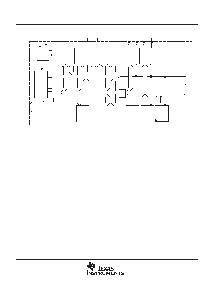
MSP430F42x0 functional block diagram
Oscillator
ACLK
SMCLK
CPU
Incl. 16 Reg.
Bus
Conv
MCB
XIN
XOUT
P6
P2
TMS
TCK
MDB, 16 Bit
MAB, 16 Bit
MCLK
4
TDI/TCLK
TDO/TDI
MAB,
4 Bit
DVCC
DVSS
AVCC
AVSS RST/NMI
P1
32KB Flash
24KB Flash
16KB Flash
256B RAM
SD16_A
16-Bit
Watchdog
Timer+
15/16-Bit
Timer_A3
3 CC Reg
I/O Port 1/2
16 I/Os,
with
Interrupt
Capability
I/O Port 5/6
16 I/Os
POR
Brownout
Basic
Timer 1
1 Interrupt
Vector
LCD_A
56
Segments
1,2,3,4 MUX
fLCD
FLL+
8
8
8
8
MDB, 8 Bit
MDB, 16-Bit
DAC12
12-Bit
1 Channel
Voltage out
Test
JTAG
Emulation
Module
MAB, 16-Bit
P5

MSP430F42x0
MIXED SIGNAL MICROCONTROLLER
SLAS455C - MARCH 2005 - REVISED AUGUST 2005
5
POST OFFICE BOX 655303
∑
DALLAS, TEXAS 75265
MSP430F42x0 Terminal Functions
TERMINAL
NAME
DL
NO.
RGZ
NO.
I/O
DESCRIPTION
TDO/TDI
1
43
I/O
Test data output port. TDO/TDI data output or programming data input terminal
TDI/TCLK
2
44
I
Test data input or test clock input. The device protection fuse is connected to TDI/TCLK.
TMS
3
45
I
Test mode select. TMS is used as an input port for device programming and test.
TCK
4
46
I
Test clock. TCK is the clock input port for device programming and test.
RST/NMI
5
47
I
General-purpose digital I/O / reset input or nonmaskable interrupt input port
DVCC
6
48
Digital supply voltage, positive terminal
DVSS
7
1
Digital supply voltage, negative terminal
XIN
8
2
I
Input terminal of crystal oscillator XT1
XOUT
9
3
O
Output terminal of crystal oscillator XT1
AVSS
10
4
Analog supply voltage, negative terminal
AVCC
11
5
Analog supply voltage, positive terminal
VREF
12
6
I/O
Analog reference voltage
P6.0/A0+
13
7
I/O
General-purpose digital I/O / analog input A0+
P6.1/A0-
14
8
I/O
General-purpose digital I/O / analog input A0-
P6.2/A1+
15
9
I/O
General-purpose digital I/O / analog input A1+
P6.3/A1-
16
10
I/O
General-purpose digital I/O / analog input A1-
P6.4
17
11
I/O
General-purpose digital I/O
P6.5
18
12
I/O
General-purpose digital I/O
P6.6
19
13
I/O
General-purpose digital I/O
P6.7
20
14
I/O
General-purpose digital I/O
P1.7/A2+
21
15
I/O
General-purpose digital I/O / analog input A2+
P1.6/A2-
22
16
I/O
General-purpose digital I/O / analog input A2-
P1.5/TACLK/ACLK/A3+
23
17
I/O
General-purpose digital I/O / Timer_A, clock signal TACLK input /
ACLK output (divided by 1, 2, 4, or 8) / analog input A3+
P1.4/A3-/DAC0
24
18
I/O
General-purpose digital I/O / analog input A3- / DAC12 output
P1.3/TA2/A4+
25
19
I/O
General-purpose digital I/O / Timer_A, Capture: CCI2A, compare: Out2 output /
analog input A4+
P1.2/TA1/A4-
26
20
I/O
General-purpose digital I/O / Timer_A, Capture: CCI1A, compare: Out1 output /
analog input A4-
P1.1/TA0/MCLK
27
21
I/O
General-purpose digital I/O / Timer_A. Capture: CCI0B / MCLK output. Note: TA0 is only an
input on this pin / BSL Receive
P1.0/TA0
28
22
I/O
General-purpose digital I/O / Timer_A. Capture: CCI0A input, compare: Out0 output / BSL
Transmit
LCDREF/R13
29
23
External LCD reference voltage input / input port of third most positive analog LCD level (V4
or V3)
LCDCAP/R23
30
24
Capacitor connection for LCD charge pump /
input port of second most positive analog LCD level (V2)
P5.1/S0
31
25
I/O
General-purpose digital I/O / LCD segment output 0
P5.0/S1
32
26
I/O
General-purpose digital I/O / LCD segment output 1
P5.5/S2
33
27
I/O
General-purpose digital I/O / LCD segment output 2
P5.6/S3
34
28
I/O
General-purpose digital I/O / LCD segment output 3
P5.7/S4
35
29
I/O
General-purpose digital I/O / LCD segment output 4
S5
36
30
O
LCD segment output 5
P2.7/S6
37
31
I/O
General-purpose digital I/O / LCD segment output 6
P2.6/S7
38
32
I/O
General-purpose digital I/O / LCD segment output 7