Document Outline
- FEATURES
- APPLICATIONS
- DESCRIPTION
- ABSOLUTE MAXIMUM RATINGS
- PACKAGE/ORDERING INFORMATION
- PIN CONFIGURATION
- ELECTRICAL CHARACTERISTICS
- TYPICAL CHARACTERISTICS
- APPLICATIONS INFORMATION
- THEORY OF OPERATION
- DISCUSSION OF PERFORMANCE
- DC GAIN TRANSFER CHARACTERISTICS
- OFFSET VOLTAGE AND NOISE
- INCREASING BANDWIDTH AT HIGH GAINS
- CIRCUIT LAYOUT AND BASIC OPERATION
- ESD PROTECTION
- OUTPUT DRIVE CAPABILITY
- THERMAL CONSIDERATIONS
- DRIVING CAPACITIVE LOADS
- COMPENSATION
- DISTORTION
- DIFFERENTIAL GAIN AND PHASE
- DESIGN-IN TOOLS
- PACKAGE DRAWINGS
- D (R-PDSO-G**) PLASTIC SMALL-OUTLINE PACKAGE
- DBV (R-PDSO-G5) PLASTIC SMALL-OUTLINE
- P (R-PDIP-T8) PLASTIC DUAL-IN-LINE

FEATURES
q
UNITY-GAIN STABLE BANDWIDTH: 900MHz
q
LOW POWER: 50mW
q
LOW DIFFERENTIAL GAIN/PHASE ERRORS:
0.025%/0.02
∞
q
HIGH SLEW RATE: 1700V/
µ
s
q
GAIN FLATNESS: 0.1dB to 135MHz
q
HIGH OUTPUT CURRENT (80mA)
Wideband, Low-Power, Current-Feedback
Operational Amplifier
APPLICATIONS
q
MEDICAL IMAGING
q
HIGH-RESOLUTION VIDEO
q
HIGH-SPEED SIGNAL PROCESSING
q
COMMUNICATIONS
q
PULSE AMPLIFIERS
q
ADC/DAC GAIN AMPLIFIER
q
MONITOR PREAMPLIFIER
q
CCD IMAGING AMPLIFIER
DESCRIPTION
The OPA658 is an ultra-wideband, low power current feed-
back video operational amplifier featuring high slew rate and
low differential gain/phase error. The current feedback de-
sign allows for superior large signal bandwidth, even at high
gains. The low differential gain/phase errors, wide bandwidth
and low quiescent current make the OPA658 a perfect
choice for numerous video, imaging and communications
applications.
The OPA658 is optimized for low gain operation and is also
available in dual (OPA2658) configurations.
C
COMP
Current Mirror
In
≠
In
+
V
OUT
I
BIAS
I
BIAS
+V
S
≠V
S
Current Mirror
Buffer
OPA658
OPA658
OPA658
SBOS045A ≠ MARCH 1994 ≠ REVISED JUNE 2003
www.ti.com
PRODUCTION DATA information is current as of publication date.
Products conform to specifications per the terms of Texas Instruments
standard warranty. Production processing does not necessarily include
testing of all parameters.
Copyright © 1994-2003, Texas Instruments Incorporated
All trademarks are the property of their respective owners.
Please be aware that an important notice concerning availability, standard warranty, and use in critical applications of
Texas Instruments semiconductor products and disclaimers thereto appears at the end of this data sheet.

OPA658
2
SBOS045A
www.ti.com
1
2
3
4
8
7
6
5
NC
+V
S
Output
NC
NC
≠Input
+Input
≠V
S
NC = No Connection
1
2
3
5
4
+V
S
≠Input
Output
≠V
S
+Input
Top View
DIP, SO
PIN CONFIGURATION
ABSOLUTE MAXIMUM RATINGS
(1)
Supply ...............................................................................................
±
5.5V
Internal Power Dissipation ........................... See Thermal Characteristics
Differential Input Voltage ..................................................................
±
1.2V
Input Voltage Range ............................................................................
±
V
S
Storage Temperature Range: P, U, UB, N .................... ≠40
∞
C to +125
∞
C
Lead Temperature (soldering, 10s) ............................................... +300
∞
C
(soldering, SO 3s) .......................................... +260
∞
C
Junction Temperature (T
J
) ............................................................ +150
∞
C
NOTE: (1) Stresses above those listed under "Absolute Maximum Ratings"
may cause permanent damage to the device. Exposure to absolute maximum
conditions for extended periods may affect device reliability.
ELECTROSTATIC
DISCHARGE SENSITIVITY
This integrated circuit can be damaged by ESD. Texas Instru-
ments recommends that all integrated circuits be handled with
appropriate precautions. Failure to observe proper handling
and installation procedures can cause damage.
ESD damage can range from subtle performance degrada-
tion to complete device failure. Precision integrated circuits
may be more susceptible to damage because very small
parametric changes could cause the device not to meet its
published specifications.
SPECIFIED
PACKAGE
TEMPERATURE
PACKAGE
ORDERING
TRANSPORT
PRODUCT
PACKAGE-LEAD
DESIGNATOR
(1)
RANGE
MARKING
NUMBER
MEDIA, QUANTITY
OPA658
SO-8 Surface-Mount
D
≠40
∞
C to +85
∞
C
OPA658U
OPA658U
Rails, 100
"
"
"
"
"
OPA658U/2K5
Tape and Reel, 2500
OPA658
SO-8 Surface-Mount
D
≠40
∞
C to +85
∞
C
OPA658UB
OPA658UB
Rails, 100
"
"
"
"
"
OPA658UB/2K5
Tape and Reel, 2500
OPA658
SOT23-5
DBV
≠40
∞
C to +85
∞
C
A58
OPA658N/250
Tape and Reel, 250
"
"
"
"
"
OPA658N/3K
Tape and Reel, 3000
OPA658
DIP-8
P
≠40
∞
C to +85
∞
C
OPA658P
OPA658P
Rails, 50
NOTE: (1) For the most current specifications and package information, refer to our web site at www.ti.com.
PACKAGE/ORDERING INFORMATION
Top View
SOT23

OPA658
3
SBOS045A
www.ti.com
FREQUENCY RESPONSE
Closed-Loop Bandwidth
(1)
G = +1
(2)
900
T
(3)
MHz
G = +2
680
400
T
MHz
G = +5
370
T
MHz
G = +10
200
T
MHz
Slew Rate
(4)
G = +2, 2V Step
1700
1000
T
V/
µ
s
At Minimum Specified Temperature
1500
900
T
V/
µ
s
Settling Time: 0.01%
G = +2, 2V Step
15
T
ns
0.1%
G = +2, 2V Step
11.5
T
ns
1%
G = +2, 2V Step
6
T
ns
Spurious-Free Dynamic Range
f = 5MHz, G = +2, V
O
= 2V
PP
68
T
dBc
f = 20MHz, G= +2, V
O
= 2V
PP
56
T
dBc
3rd-Order Intercept Point
f = 10MHz, 4dBm Each Tone
40
T
dBm
Differential Gain
G = +2, NTSC, V
O
= 1.4V
PP
, R
L
= 150
0.025
T
%
Differential Phase
G = +2, NTSC, V
O
= 1.4V
PP
, R
L
= 150
0.02
T
degrees
Bandwidth for 0.1dB Flatness
G = +2
135
(5)
T
MHz
OFFSET VOLTAGE
Input Offset Voltage
V
CM
= 0V
±
3
±
5.5
±
2
±
4.5
mV
Over Temperature Range
±
5
±
8
±
4
±
7
mV
Power-Supply Rejection Ratio
V
S
=
±
4.7 to
±
5.5V
55
64
58
67
dB
INPUT BIAS CURRENT
Noninverting
V
CM
= 0V
±
5.7
±
30
T
±
18
µ
A
Over Temperature Range
±
10
±
80
T
±
35
µ
A
Inverting
V
CM
= 0V
±
1.1
±
35
T
T
µ
A
Over Temperature Range
±
30
±
75
T
T
µ
A
NOISE
Input Voltage Noise Density
f = 100Hz
16
T
nV/
Hz
f = 2kHz
4.9
T
nV/
Hz
f = 10kHz
3.2
T
nV/
Hz
f = 1MHz
3.2
T
nV/
Hz
f
B
= 100Hz to 200MHz
45.3
T
µ
Vrms
Input Bias Current Noise Density
Inverting: f = 1MHz
32
T
pA/
Hz
Noninverting: f = 1MHz
11.9
T
pA/
Hz
INPUT VOLTAGE RANGE
Common-Mode Input Range
Over Temperature Range
±
2.5
±
2.9
T
T
V
Common-Mode Rejection
V
CM
=
±
1V
45
50
T
T
dB
INPUT IMPEDANCE
Noninverting
500 || 1
T
k
|| pF
Inverting
50
T
OPEN-LOOP TRANSRESISTANCE
Open-Loop Transresistance
V
O
=
±
2V, R
L
= 100
150
190
200
250
k
Over Temperature Range
V
O
=
±
2V, R
L
= 100
100
150
k
OUTPUT
Voltage Output
No Load
±
2.7
±
2.9
T
T
V
Over Temperature Range
±
2.5
±
2.75
T
T
V
Voltage Output
R
L
= 250
±
2.7
±
2.9
T
T
V
Over Temperature Range
±
2.5
±
2.7
T
T
V
Voltage Output
R
L
= 100
±
2.2
±
2.8
T
T
V
Over Temperature Range
±
2.0
±
2.5
T
T
V
Output Current, Sourcing
80
120
T
T
mA
Over Temperature
70
T
mA
Output Current, Sinking
60
80
T
T
mA
Over Temperature
35
T
mA
Short Circuit Current
150
T
mA
Output Resistance
0.1MHz, G = +2
0.02
T
POWER SUPPLY
Specified Operating Voltage
±
5
T
V
Operating Voltage Range
±
4.5
±
5.5
T
T
V
Quiescent Current
V
S
=
±
5V
±
5
±
7.75
±
4.5
±
5.75
mA
Over Temperature Range
±
5.5
±
8.5
±
4.7
±
6.5
mA
TEMPERATURE RANGE
Specification: P, U, N, UB
≠40
+85
T
T
∞
C
Thermal Resistance,
JA
P
DIP-8
100
T
∞
C/W
U
SO-8
125
T
∞
C/W
N
SOT23-5
150
T
∞
C/W
(1) Frequency response can be strongly influenced by PC board parasitics. The demonstration boards show low parasitic layouts for this part. Refer to the
demonstration board layout for details.
(2) At G = +1, R
FB
= 560
for DIP and 402
for SO-8.
(3) An asterisk (
T
) specifies the same value as the grade to the left.
(4) Slew rate is rate of change from 10% to 90% of output voltage step.
(5) This specification is PC board layout dependent.
ELECTRICAL CHARACTERISTICS
At T
A
= +25
∞
C, V
S
=
±
5V, R
L
= 100
,
and R
FB
= 402
,
unless otherwise noted.
OPA658P, U, N
OPA658UB
PARAMETER
CONDITION
MIN
TYP
MAX
MIN
TYP
MAX
UNITS

OPA658
4
SBOS045A
www.ti.com
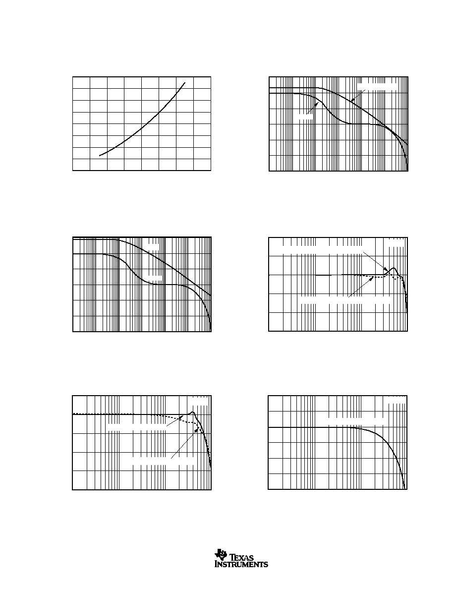
TYPICAL CHARACTERISTICS
At T
A
= +25
∞
C, V
S
=
±
5V, R
L
= 100
, and R
FB
= 402
, unless otherwise noted.
POWER-SUPPLY REJECTION RATIO AND
COMMON-MODE REJECTION vs TEMPERATURE
75
70
65
60
55
50
45
≠75
≠50
≠25
0
25
50
75
100
125
PSRR , CMR (dB)
CMR
PSR≠
Temperature (
∞
C)
PSR+
PSRR
55
50
45
40
35
30
25
≠4
≠3
≠2
≠1
0
1
2
3
4
COMMON-MODE REJECTION
vs INPUT COMMON-MODE VOLTAGE
Common-Mode Rejection (dB)
Common-Mode Voltage (V)
SUPPLY CURRENT vs TEMPERATURE
5.5
5.0
4.5
4.0
3.5
≠75
≠50
≠25
0
25
50
75
100
125
Ambient Temperature (
∞
C)
Supply Current (
±
mA)
120
110
100
90
80
70
≠75
≠50
≠25
0
25
50
75
100
125
OUTPUT CURRENT vs TEMPERATURE
Ambient Temperature (
∞
C)
Output Current (
±
mA)
I
O
≠
I
O
+
3.20
3.10
3.00
2.90
2.80
2.70
2.60
2.50
2.40
2.30
OUTPUT SWING vs TEMPERATURE
Temperature (
∞
C)
≠60
≠40
≠20
0
20
40
60
80
100
Output Swing (V)
+V
O
R
L
= 250
R
L
= 100
≠V
O
≠V
O
+V
O
NONINVERTING INPUT BIAS CURRENT
vs TEMPERATURE
≠75
≠50
≠25
0
25
50
75
100
125
Ambient Temperature (
∞
C)
Noninverting Input Bias Current I
B
+ (
µ
A)
10
9
8
7
6
5
4
3
2
OPA658
5
SBOS045A
www.ti.com
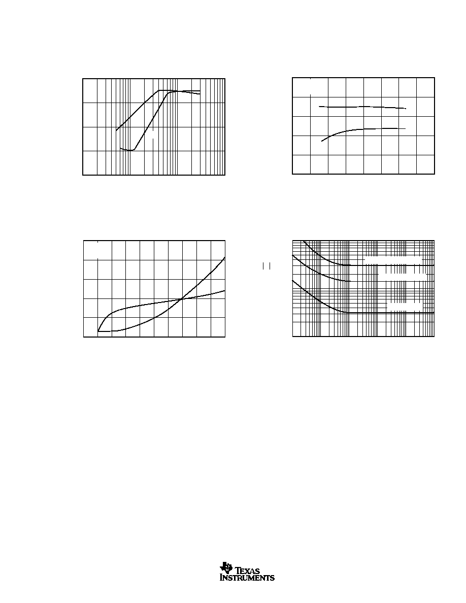
TYPICAL CHARACTERISTICS
(Cont.)
At T
A
= +25
∞
C, V
S
=
±
5V, R
L
= 100
, and R
FB
= 402
, unless otherwise noted.
INVERTING INPUT BIAS CURRENT
vs TEMPERATURE
≠75
≠50
≠25
0
25
50
75
100
125
Temperature (
∞
C)
Inverting Input Bias Current I
B
≠ (
µ
A)
2.0
1.8
1.6
1.4
1.2
1.0
0.8
0.6
0.4
10
6
10
5
10
4
10
3
10
2
10
1
1
45
0
≠45
≠90
≠135
≠180
≠225
1k
10k
100k
1M
10M
100M
1G
OPEN-LOOP TRANSIMPEDANCE AND PHASE
vs FREQUENCY
Frequency (Hz)
Transimpedance (
)
Open-Loop Phase (
∞
)
Phase
Transimpedance
OPEN-LOOP GAIN AND PHASE vs FREQUENCY
Frequency (Hz)
60
40
20
0
≠20
≠40
≠60
45
0
≠45
≠90
≠135
≠180
≠225
1k
10k
100k
1M
10M
100M
1G
Open-Loop Gain (dB)
Open-Loop Phase (
∞
)
Gain
Phase
6
3
0
≠3
≠6
≠9
1M
10M
100M
1G
CLOSED-LOOP BANDWIDTH
Frequency (Hz)
Gain (dB)
SO-8 Bandwidth = 881MHz, R
FB
= 402
G = +1
DIP Bandwidth = 949MHz, R
FB
= 560
9
6
3
0
≠3
≠6
1M
10M
100M
1G
CLOSED-LOOP BANDWIDTH
Frequency (Hz)
Gain (dB)
DIP Bandwidth = 682MHz
SO-8 Bandwidth = 680MHz
G = +2
20
17
14
11
8
5
2
1M
10M
100M
1G
CLOSED-LOOP BANDWIDTH
Frequency (Hz)
Gain (dB)
SO-8/DIP Bandwidth= 372MHz
G = +5

OPA658
6
SBOS045A
www.ti.com
TYPICAL CHARACTERISTICS
(Cont.)
At T
A
= +25
∞
C, V
S
=
±
5V, R
L
= 100
, and R
FB
= 402
, unless otherwise noted.
26
23
20
17
14
11
8
1M
10M
100M
1G
CLOSED-LOOP BANDWIDTH
Frequency (Hz)
Gain (dB)
SO-8/DIP Bandwidth = 200MHz
G = +10
160
120
80
40
0
≠40
≠80
≠120
≠160
Time (5ns/div)
SMALL-SIGNAL TRANSIENT RESPONSE
Output Voltage (mV)
G = +2
40
35
30
25
20
15
10
10
100
90
80
70
60
50
40
30
20
RECOMMENDED ISOLATION RESISTANCE
vs CAPACITIVE LOAD
Capacitive Load (pF)
Isolation Resistance
G = +2
OPA658
C
L
1k
R
ISO
402
402
1.6
1.2
0.8
0.4
0
≠0.4
≠0.8
≠1.2
≠1.6
LARGE-SIGNAL TRANSIENT RESPONSE
Time (5ns/div)
Output Voltage (V)
G = +2
≠50
≠55
≠60
≠65
≠70
≠75
≠80
≠85
≠90
≠95
≠100
100k
1M
10M
100M
HARMONIC DISTORTION vs FREQUENCY
Frequency (Hz)
Harmonic Distortion (dBc)
2f
O
3f
O
5MHz HARMONIC DISTORTION vs OUTPUT SWING
Output Swing (V
PP
)
≠60
≠65
≠70
≠75
≠80
≠85
≠90
≠95
≠100
0
1
2
3
4
Harmonic Distortion (dBc)
2f
O
3f
O
G = +2
OPA658
7
SBOS045A
www.ti.com
TYPICAL CHARACTERISTICS
(Cont.)
At T
A
= +25
∞
C, V
S
=
±
5V, R
L
= 100
, and R
FB
= 402
, unless otherwise noted.
10MHz HARMONIC DISTORTION vs OUTPUT SWING
Output Swing (V
PP
)
≠60
≠70
≠80
≠90
≠100
0.01
0.1
2f
O
1
4V
10
Harmonic Distortion (dBc)
3f
O
≠60
≠65
≠70
≠75
≠80
≠85
≠75
≠50
≠25
0
25
50
75
100
125
Temperature (
∞
C)
HARMONIC DISTORTION vs TEMPERATURE
Harmonic Distortion (dBc)
3f
O
2f
O
V
O
= 2V
PP
G = +2
HARMONIC DISTORTION vs GAIN
Noninverting Gain (V/V)
≠50
≠55
≠60
≠65
≠70
≠75
Harmonic Distortion (dBc)
0
1
2
3
4
5
6
7
8
9
10
3f
O
2f
O
f
O
= 5MHz
V
O
= 2V
PP
INPUT VOLTAGE AND CURRENT NOISE
vs FREQUENCY
Frequency (Hz)
100
10
1
Voltage Noise (nV/
Hz)
Current Noise (pA/
Hz)
10
2
10
3
10
4
10
5
10
6
10
7
Noninverting Noise
Inverting Current Noise
Voltage Noise

OPA658
8
SBOS045A
www.ti.com
For noninverting operation, the input signal is applied to the
noninverting (high impedance buffer) input. The output (buffer)
error current (I
E
) is generated at the low impedance inverting
input. The signal generated at the output is fed back to the
inverting input such that the overall gain is (1 + R
FB
/R
FF
).
Where a voltage-feedback amplifier has two symmetrical
high impedance inputs, a current-feedback amplifier has a
low inverting (buffer output) impedance and a high noninverting
(buffer input) impedance.
The closed-loop gain for the OPA658 can be calculated
using Equations 1 and 2.
Inverting Gain
R
R
Loop Gain
FB
FF
=
-
+
1
1
(1)
Noninverting Gain
R
R
Loop Gain
where Loop Gain
T
R
R
R
FB
FF
O
FB
RS
FB
FF
=
+
+
=
+
+
1
1
1
1
(2)
At higher gains, the small value inverting input impedance
causes an apparent loss in bandwidth. This can be seen from
Equation 3.
f
f
ACTUAL
A
S
FB
FB
FF
BW
BW
R
R
R
R
V
[
]
◊
(
)
+
◊
+
= +
(
)
2
1 25
1
1
.
(3)
This loss in bandwidth at high gains can be corrected without
affecting stability by lowering the value of the feedback
resistor from the specified value of 402
.
OFFSET VOLTAGE AND NOISE
The output offset is the algebraic sum of the input offset
voltage and bias current errors. The output offset for the
model of Figure 2 is calculated by Equation 4.
Output Offset Voltage
Ib
R
R
R
V
R
R
Ib
R
N
N
FB
FF
IO
FB
FF
N
FB
=
±
◊
+
±
+
±
◊
1
1
(4)
APPLICATIONS INFORMATION
THEORY OF OPERATION
Conventional op amps depend on feedback to drive their
inputs to the same potential, however the current-feedback
op amp's inverting and noninverting inputs are connected by
a unity-gain buffer, thus enabling the inverting input to
automatically assume the same potential as the noninverting
input. This results in very low impedance at the inverting
input to sense the feedback as an error current signal.
DISCUSSION OF PERFORMANCE
The OPA658 is a low-power, unity-gain stable, current-
feedback operational amplifier which operates on
±
5V power
supply. The current-feedback architecture offers the follow-
ing important advantages over voltage-feedback architec-
tures: (1) the high slew rate allows the large-signal perfor-
mance to approach the small-signal performance, and (2)
there is very little bandwidth degradation at higher gain
settings.
The current-feedback architecture of the OPA658 provides
the traditional strength of excellent large-signal response
plus wide bandwidth, making it a good choice for use in high-
resolution video, medical imaging and Digital-to-Analog Con-
verter (DAC) I/V Conversion. The low-power requirements
make it an excellent choice for numerous portable applica-
tions.
DC GAIN TRANSFER CHARACTERISTICS
The circuit in Figure 1 shows the equivalent circuit for
calculating the DC gain. When operating the device in the
inverting mode, the input signal error current (I
E
) is amplified
by the open loop transimpedance gain (T
O
). The output
signal generated is equal to T
O
x I
E
. Negative feedback is
applied through R
FB
such that the device operates at a gain
equal to ≠R
FB
/R
FF
.
FIGURE 1. Equivalent Circuit.
FIGURE 2. Output Offset Voltage Equivalent Circuit.
V
O
T
O
C
C
L
S
R
S
(50
)
C
1
V
I
V
N
R
FF
R
FB
I
E
+
≠
R
FB
R
FF
Ib
I
R
N
Ib
N
V
IO

OPA658
9
SBOS045A
www.ti.com
The feedback resistor value acts as the frequency response
compensation element for a current-feedback type amplifier.
The 402
used in setting the specification achieves a nomi-
nal maximally-flat butterworth response while assuming a
2pF output pin parasitic. Increasing the feedback resistor will
overcompensate the amplifier, rolling off the frequency re-
sponse, while decreasing it will decrease phase margin,
peaking up the frequency response. Note that a noninverting,
unity-gain buffer application still requires a feedback resistor
for stability (560
for SO-8, 402
for DIP, and 324
for
SOT23).
d) Connections to other wideband devices on the board
may be made with short direct traces or through onboard
transmission lines. For short connections, consider the trace
and the input to the next device as a lumped capacitive load.
Relatively wide traces (50 mils to 100 mils) should be used,
preferably with ground and power planes opened up around
them. Estimate the total capacitive load and set R
ISO
from the
plot of recommended R
ISO
vs capacitive load. Low parasitic
loads may not need an R
ISO
since the OPA658 is nominally
compensated to operate with a 2pF parasitic load.
If a long trace is required and the 6dB signal loss intrinsic to
doubly-terminated transmission lines is acceptable, imple-
ment a matched impedance transmission line using microstrip
or stripline techniques (consult an ECL design handbook for
microstrip and stripline layout techniques). A 50
environ-
ment is not necessary onboard, and in fact a higher imped-
ance environment will improve distortion as shown in the
distortion vs load plot. With a characteristic impedance de-
fined based on board material and desired trace dimensions,
a matching series resistor into the trace from the output of the
amplifier is used as well as a terminating shunt resistor at the
input of the destination device. Remember also that the
terminating impedance will be the parallel combination of the
shunt resistor and the input impedance of the destination
device; the total effective impedance should match the trace
impedance. Multiple destination devices are best handled as
separate transmission lines, each with their own series and
shunt terminations.
If the 6dB attenuation loss of a doubly-terminated line is
unacceptable, a long trace can be series-terminated at the
source end only. This will help isolate the line capacitance
from the op amp output, but will not preserve signal integrity
as well as a doubly-terminated line. If the shunt impedance
at the destination end is finite, there will be some signal
attenuation due to the voltage divider formed by the series
and shunt impedances.
e) Socketing a high-speed part like the OPA658 is not
recommended. The additional lead length and pin-to-pin
capacitance introduced by the socket creates an extremely
troublesome parasitic network which can make it almost
impossible to achieve a smooth, stable response. Best re-
sults are obtained by soldering the part onto the board. If
socketing for the DIP package is desired, high-frequency,
flush-mount pins (for instance, McKenzie Technology #710C)
can give good results.
If all terms are divided by the gain (1 + R
FB
/R
FF
) it can be
observed that input referred offsets improve as gain in-
creases. The effective noise at the output can be determined
by taking the root sum of the squares of Equation 4 and
applying the spectral noise values found in the Typical
Characteristics section. This applies to noise from the op
amp only. Note that both the noise figure (NF) and the
equivalent input offset voltages improve as the closed-loop
gain increases (by keeping R
FB
fixed and reducing R
FF
with
R
N
= 0
).
INCREASING BANDWIDTH AT HIGH GAINS
The closed-loop bandwidth can be extended at high gains by
reducing the value of the feedback resistor R
FB
. This band-
width reduction is caused by the feedback current being split
between R
S
and R
FF
(refer to Figure 1). As the gain increases
(for a fixed R
FB
), more feedback current is shunted through
R
FF
, which reduces closed-loop bandwidth.
CIRCUIT LAYOUT AND BASIC OPERATION
Achieving optimum performance with a high-frequency am-
plifier such as the OPA658 requires careful attention to
layout parasitics and selection of external components. Rec-
ommendations for PC board layout and component selection
include:
a) Minimize parasitic capacitance to any ac ground for all
of the signal I/O pins. Parasitic capacitance on the output and
inverting input pins can cause instability; on the noninverting
input it can react with the source impedance to cause
unintentional bandlimiting. To reduce unwanted capacitance,
a window around the signal I/O pins should be opened in all
of the ground and power planes. Otherwise, ground and
power planes should be unbroken elsewhere on the board.
b) Minimize the distance (< 0.25") from the two power pins
to high-frequency 0.1
µ
F decoupling capacitors. At the pins,
the ground and power-plane layout should not be in close
proximity to the signal I/O pins. Avoid narrow power and
ground traces to minimize inductance between the pins and
the decoupling capacitors. Larger (2.2
µ
F to 6.8
µ
F) decou-
pling capacitors, effective at lower frequencies, should also
be used. These may be placed somewhat farther from the
device and may be shared among several devices in the
same area of the PC board.
c) Careful selection and placement of external compo-
nents will preserve the high-frequency performance of
the OPA658. Resistors should be a very low reactance type.
Surface-mount resistors work best and allow a tighter overall
layout. Metal film or carbon composition axially-leaded resis-
tors can also provide good high-frequency performance.
Again, keep their leads as short as possible. Never use wire-
wound type resistors in a high-frequency application.
Since the output pin and the inverting input pin are most
sensitive to parasitic capacitance, always position the feed-
back and series output resistor, if any, as close as possible
to the package pins. Other network components, such as
noninverting input termination resistors, should also be placed
close to the package.

OPA658
10
SBOS045A
www.ti.com
The OPA658 is nominally specified for operation using
±
5V power supplies. A 10% tolerance on the supplies, or an
ECL ≠5.2V for the negative supply, is within the maximum
specified total supply voltage of 11V. Higher supply voltages
can break down internal junctions possibly leading to cata-
strophic failure. Single-supply operation is possible as long
as common-mode voltage constraints are observed. The
common-mode input and output voltage specifications can
be interpreted as a required headroom to the supply voltage.
Observing this input and output headroom requirement will
allow non-standard or single-supply operation. Figure 3 shows
one approach to single-supply operation.
THERMAL CONSIDERATIONS
The OPA658 will not require heatsinking under most operat-
ing conditions. Maximum desired junction temperature will
set a maximum allowed internal power dissipation as de-
scribed below. In no case should the maximum junction
temperature be allowed to exceed 175
∞
C.
Operating junction temperature (T
J
) is given by T
A
+ P
D
◊
JA
.
The total internal power dissipation (P
D
) is the sum of
quiescent power (P
DQ
) and additional power dissipated in the
output stage (P
DL
) to deliver load power. Quiescent power is
simply the specified no-load supply current times the total
supply voltage across the part. P
DL
will depend on the
required output signal and load but would, for a grounded
resistive load, be at a maximum when the output is fixed at
a voltage equal to 1/2 either supply voltage (for equal bipolar
supplies). Under this condition P
DL
= V
S
2
/(4
◊
R
L
) where R
L
includes feedback network loading.
Note that it is the power in the output stage and not into the
load that determines internal power dissipation.
As an example, compute the maximum T
J
for an OPA658N
at A
V
= +2, R
L
= 100
, R
FB
= 402
,
±
V
S
=
±
5V, and the
specified maximum T
A
= +85
∞
C.
P
D
= 10V
◊
8.5mA + 5
2
/[4
◊
(100
|| 804
)] = 155mW
Maximum T
J
= 85
∞
C + 0.155W
◊
150
∞
C/W = 108
∞
C
DRIVING CAPACITIVE LOADS
The OPA658's output stage has been optimized to drive low
resistive loads. Capacitive loads, however, will decrease the
amplifier's phase margin which may cause high-frequency
peaking or oscillations. Capacitive loads greater than 5pF
should be buffered by connecting a small resistance, usually
10
to 35
, in series with the output as illustrated in Figure 5.
This is particularly important when driving high capacitance
loads such as flash ADCs.
In general, capacitive loads should be minimized for opti-
mum high-frequency performance. Coaxial lines can be
driven if the cable is properly terminated. The capacitance of
coaxial cable (29pF/foot for RG-58) will not load the amplifier
when the coaxial cable or transmission line is terminated with
its characteristic impedance.
FIGURE 4. Closed-Loop Output Impedance vs Frequency.
ESD PROTECTION
ESD static damage has been well recognized for MOSFET
devices, but any semiconductor device deserves protection
from this potentially damaging source. This is particularly true
for very high-speed, fine geometry processes.
ESD static damage can cause subtle changes in amplifier
input characteristics without necessarily destroying the de-
vice. In precision operational amplifiers, this may cause a
noticeable degradation of offset voltage and drift. Therefore,
static protection is strongly recommended when handling the
OPA658.
OUTPUT DRIVE CAPABILITY
The OPA658 has been optimized to drive 75
and 100
resistive loads. The device can drive 2V
PP
into a 75
load.
This high-output drive capability makes the OPA658 an ideal
choice for a wide range of RF, IF, and video applications. In
many cases, additional buffer amplifiers are unneeded.
Many demanding high-speed applications such as Analog-to-
Digital Converter (ADC)/DAC buffers require op amps with low
wideband output impedance. For example, low output imped-
ance is essential when driving the signal-dependent capaci-
tances at the inputs of flash ADCs. As shown in Figure 4, the
OPA658 maintains very low closed-loop output impedance
over frequency. Closed-loop output impedance increases with
frequency since loop gain is decreasing with frequency.
FIGURE 3. Single-Supply Operation.
402
OPA658
V
AC
402
R
L
+V
S
+V
S
V
S
2
R
OUT
V
S
2
V
OUT
= + A
V
V
AC
A
V
= +2
100
10
1
0.1
0.01
0.001
10k
100k
1M
10M
100M
Output Impedance (
)
Frequency (Hz)
G = +2

OPA658
11
SBOS045A
www.ti.com
appear at f
O
±
3
◊
Df. The 2-tone, 3rd-order spurious plot
shown in Figure 7 indicates how far below these two equal
power, closely-spaced tones the intermodulation spurious
will be. The single-tone power is at a matched 50
load. The
unique design of the OPA658 provides much greater spuri-
ous free range than what a 2-tone, 3rd-order intermodulation
intercept specification would predict. This can be seen in
Figure 7 as the spurious-free range actually increases at the
higher output power levels.
COMPENSATION
The OPA658 is internally compensated and is stable in unity
gain with a phase margin of approximately 62
∞
, and approxi-
mately 64
∞
in a gain of +2V/V when used with the recom-
mended feedback resistor value. Frequency response for
other gains are shown in the Typical Characteristics.
The high-frequency response of the OPA658 in a good
layout is very flat with frequency.
DISTORTION
The OPA658's Harmonic Distortion characteristics into a
100
load are shown versus frequency and power output in
the Typical Characteristics. Distortion can be further im-
proved by increasing the load resistance as illustrated in
Figure 6. Remember to include the contribution of the feed-
back resistance when calculating the effective load resis-
tance seen by the amplifier.
Narrowband communication channel requirements will ben-
efit from the OPA658's wide bandwidth and low
intermodulation distortion on low quiescent power. If output
signal power at two closely spaced frequencies is required,
3rd-order nonlinearities in any amplifier will cause spurious
power at frequencies very near the two fundamental frequen-
cies. If the two test frequencies, f
1
and f
2
, are specified in
terms of average and delta frequency, f
O
= (f
1
+ f
2
)/2 and
Df =
f
2
≠ f
1
, the two, 3rd-order, close-in spurious tones will
DIFFERENTIAL GAIN AND PHASE
Differential Gain (dG) and Differential Phase (dP) are among
the more important specifications for video applications. dG
is defined as the percent change in closed-loop gain over a
specified change in output voltage level. dP is defined as the
change in degrees of the closed-loop phase over the same
output voltage change. Both dG and dP are specified at the
NTSC sub-carrier frequency of 3.58MHz and the PAL sub-
carrier of 4.43MHz. All NTSC measurements were performed
using a Tektronix model VM700A Video Measurement Set.
dG/dP of the OPA658 were measured with the amplifier in a
gain of +2V/V with 75
input impedance and the output
back-terminated in 75
. The input signal selected from the
generator was a 0V to 1.4V modulated ramp with sync pulse.
With these conditions the test circuit shown in Figure 8
delivered a 100IRE modulated ramp to the 75
input of the
videoanalyzer. The signal averaging feature of the analyzer
was used to establish a reference against which the perfor-
FIGURE 5. Driving Capacitive Loads.
FIGURE 6. 5MHz Harmonic Distortion vs Load Resistance.
FIGURE 7. 3rd-Order Spurious Level vs Frequency.
FIGURE 8. Configuration for Testing Differential Gain/Phase.
OPA658
50
R
ISO
R
L
C
L
10
to 35
402
402
≠55
≠60
≠65
≠70
≠75
≠80
≠85
5MHz HARMONIC DISTORTION vs
LOAD RESISTANCE (G = +2)
Load Resistance (
)
Harmonic Distortion (dBc)
10
100
1k
G = +2
V
O
= 2V
PP
f
O
= 5MHz
3f
O
2f
O
≠65
≠70
≠75
≠80
≠85
≠90
≠18 ≠16 ≠14 ≠12 ≠10
≠8
≠6
≠4
≠2
0
2
4
3rd-Order Spurious Level (dBc)
2-TONE, 3RD-ORDER SPURIOUS LEVELS
Single-Tone Power (dBm)
20MHz
10MHz
5MHz
OPA658
75
75
402
402
75
75
TEK TSG 130A
TEK VM700A

OPA658
12
SBOS045A
www.ti.com
mance of the amplifier was measured. Signal averaging was
also used to measure the dg and dp of the test signal in order
to eliminate the generator's contribution to measured ampli-
fier performance. Typical performance of the OPA658 is
0.025% differential gain and 0.02
∞
differential phase to both
NTSC and PAL standards.
DESIGN-IN TOOLS
DEMONSTRATION BOARDS
Several PC boards are available to assist in the initial
evaluation of circuit performance using the OPA658 in its
three package styles. All of these are available free as an
unpopulated PC board delivered with descriptive documen-
tation. The summary information for these boards is shown
in Table I.
To request any of these boards, check the Texas Instru-
ments web site at www.ti.com.
BOARD
LITERATURE
PART
REQUEST
PRODUCT
PACKAGE
NUMBER
NUMBER
OPA658U
SO-8
DEM-OPA68xU
SBOU009
OPA658N
SOT23-5
DEM-OPA6xxN
SBOU010
OPA658P
DIP-8
DEM-OPA68xP
SBOU008
TABLE I. Demo Board Part/Ordering Numbers.
OPA658
13
SBOS045A
www.ti.com
PACKAGE DRAWINGS
D (R-PDSO-G**)
PLASTIC SMALL-OUTLINE PACKAGE
8 PINS SHOWN
8
0.197
(5,00)
A MAX
A MIN
(4,80)
0.189
0.337
(8,55)
(8,75)
0.344
14
0.386
(9,80)
(10,00)
0.394
16
DIM
PINS **
4040047/E 09/01
0.069 (1,75) MAX
Seating Plane
0.004 (0,10)
0.010 (0,25)
0.010 (0,25)
0.016 (0,40)
0.044 (1,12)
0.244 (6,20)
0.228 (5,80)
0.020 (0,51)
0.014 (0,35)
1
4
8
5
0.150 (3,81)
0.157 (4,00)
0.008 (0,20) NOM
0
∞
≠ 8
∞
Gage Plane
A
0.004 (0,10)
0.010 (0,25)
0.050 (1,27)
NOTES: A. All linear dimensions are in inches (millimeters).
B. This drawing is subject to change without notice.
C. Body dimensions do not include mold flash or protrusion, not to exceed 0.006 (0,15).
D. Falls within JEDEC MS-012

OPA658
14
SBOS045A
www.ti.com
PACKAGE DRAWINGS (Cont.)
DBV (R-PDSO-G5)
PLASTIC SMALL-OUTLINE
0,10
M
0,20
0,95
0
∞
≠ 8
∞
0,25
0,35
0,55
Gage Plane
0,15 NOM
4073253-4/G 01/02
2,60
3,00
0,50
0,30
1,50
1,70
4
5
3
1
2,80
3,00
0,95
1,45
0,05 MIN
Seating Plane
NOTES: A. All linear dimensions are in millimeters.
B. This drawing is subject to change without notice.
C. Body dimensions do not include mold flash or protrusion.
D. Falls within JEDEC MO-178
OPA658
15
SBOS045A
www.ti.com
PACKAGE DRAWINGS (Cont.)
P (R-PDIP-T8)
PLASTIC DUAL-IN-LINE
8
4
0.015 (0,38)
Gage Plane
0.325 (8,26)
0.300 (7,62)
0.010 (0,25) NOM
MAX
0.430 (10,92)
4040082/D 05/98
0.200 (5,08) MAX
0.125 (3,18) MIN
5
0.355 (9,02)
0.020 (0,51) MIN
0.070 (1,78) MAX
0.240 (6,10)
0.260 (6,60)
0.400 (10,60)
1
0.015 (0,38)
0.021 (0,53)
Seating Plane
M
0.010 (0,25)
0.100 (2,54)
NOTES: A. All linear dimensions are in inches (millimeters).
B. This drawing is subject to change without notice.
C. Falls within JEDEC MS-001

PACKAGING INFORMATION
ORDERABLE DEVICE
STATUS(1)
PACKAGE TYPE
PACKAGE DRAWING
PINS
PACKAGE QTY
OPA658N/250
ACTIVE
SOP
DBV
5
250
OPA658N/3K
ACTIVE
SOP
DBV
5
3000
OPA658NB/250
OBSOLETE
SOP
DBV
5
OPA658NB/3K
OBSOLETE
SOP
DBV
5
OPA658P
ACTIVE
PDIP
P
8
50
OPA658U
ACTIVE
SOIC
D
8
100
OPA658U/2K5
ACTIVE
SOIC
D
8
2500
OPA658UB
ACTIVE
SOIC
D
8
100
OPA658UB/2K5
ACTIVE
SOIC
D
8
2500
(1) The marketing status values are defined as follows:
ACTIVE: Product device recommended for new designs.
LIFEBUY: TI has announced that the device will be discontinued, and a lifetime-buy period is in effect.
NRND: Not recommended for new designs. Device is in production to support existing customers, but TI does not recommend using this part in
a new design.
PREVIEW: Device has been announced but is not in production. Samples may or may not be available.
OBSOLETE: TI has discontinued the production of the device.
PACKAGE OPTION ADDENDUM
www.ti.com
3-Oct-2003

IMPORTANT NOTICE
Texas Instruments Incorporated and its subsidiaries (TI) reserve the right to make corrections, modifications,
enhancements, improvements, and other changes to its products and services at any time and to discontinue
any product or service without notice. Customers should obtain the latest relevant information before placing
orders and should verify that such information is current and complete. All products are sold subject to TI's terms
and conditions of sale supplied at the time of order acknowledgment.
TI warrants performance of its hardware products to the specifications applicable at the time of sale in
accordance with TI's standard warranty. Testing and other quality control techniques are used to the extent TI
deems necessary to support this warranty. Except where mandated by government requirements, testing of all
parameters of each product is not necessarily performed.
TI assumes no liability for applications assistance or customer product design. Customers are responsible for
their products and applications using TI components. To minimize the risks associated with customer products
and applications, customers should provide adequate design and operating safeguards.
TI does not warrant or represent that any license, either express or implied, is granted under any TI patent right,
copyright, mask work right, or other TI intellectual property right relating to any combination, machine, or process
in which TI products or services are used. Information published by TI regarding third-party products or services
does not constitute a license from TI to use such products or services or a warranty or endorsement thereof.
Use of such information may require a license from a third party under the patents or other intellectual property
of the third party, or a license from TI under the patents or other intellectual property of TI.
Reproduction of information in TI data books or data sheets is permissible only if reproduction is without
alteration and is accompanied by all associated warranties, conditions, limitations, and notices. Reproduction
of this information with alteration is an unfair and deceptive business practice. TI is not responsible or liable for
such altered documentation.
Resale of TI products or services with statements different from or beyond the parameters stated by TI for that
product or service voids all express and any implied warranties for the associated TI product or service and
is an unfair and deceptive business practice. TI is not responsible or liable for any such statements.
Following are URLs where you can obtain information on other Texas Instruments products and application
solutions:
Products
Applications
Amplifiers
amplifier.ti.com
Audio
www.ti.com/audio
Data Converters
dataconverter.ti.com
Automotive
www.ti.com/automotive
DSP
dsp.ti.com
Broadband
www.ti.com/broadband
Interface
interface.ti.com
Digital Control
www.ti.com/digitalcontrol
Logic
logic.ti.com
Military
www.ti.com/military
Power Mgmt
power.ti.com
Optical Networking
www.ti.com/opticalnetwork
Microcontrollers
microcontroller.ti.com
Security
www.ti.com/security
Telephony
www.ti.com/telephony
Video & Imaging
www.ti.com/video
Wireless
www.ti.com/wireless
Mailing Address:
Texas Instruments
Post Office Box 655303 Dallas, Texas 75265
Copyright
2003, Texas Instruments Incorporated