Document Outline
- FEATURES
- APPLICATIONS
- DESCRIPTION
- ABSOLUTE MAXIMUM RATINGS
- PACKAGE/ORDERING INFORMATION
- PIN CONFIGURATIONS
- ELECTRICAL CHARACTERISTICS: V S = ±5V
- TYPICAL CHARACTERISTICS:
- APPLICATIONS INFORMATION
- WIDEBAND VOLTAGE-FEEDBACK OPERATION
- WIDEBAND INVERTING OPERATION
- BUFFERING HIGH-PERFORMANCE ADCs
- VIDEO LINE DRIVING
- SINGLE OP AMP DIFFERENTIAL AMPLIFIER
- THREE OP AMP DIFFERENCING (Instrumentation Topology)
- DAC TRANSIMPEDANCE AMPLIFIER
- ACTIVE FILTERS
- DESIGN-IN TOOLS
- DEMONSTRATION BOARDS
- MACROMODELS AND APPLICATIONS SUPPORT
- OPERATING SUGGESTIONS
- OPTIMIZING RESISTOR VALUES
- BANDWIDTH vs GAIN
- OUTPUT DRIVE CAPABILITY
- DRIVING CAPACITIVE LOADS
- DISTORTION PERFORMANCE
- NOISE PERFORMANCE
- DC OFFSET CONTROL
- THERMAL ANALYSIS
- BOARD LAYOUT
- INPUT AND ESD PROTECTION
- PACKAGE DRAWINGS
- D (R-PDSO-G**) PLASTIC SMALL-OUTLINE PACKAGE
- DBV (R-PDSO-G5) PLASTIC SMALL-OUTLINE

OPA842
SBOS267A ≠ NOVEMBER 2002 ≠ REVISED DECEMBER 2002
www.ti.com
DESCRIPTION
The OPA842 provides a level of speed and dynamic range
previously unattainable in a monolithic op amp. Using unity-
gain stable, voltage-feedback architecture with two internal
gain stages, the OPA842 achieves exceptionally low har-
monic distortion over a wide frequency range. The "classic"
differential input provides all the familiar benefits of precision
op amps, such as bias current cancellation and very low
inverting current noise compared with wideband current
differential gain/phase performance, low-voltage noise, and
high output current drive make the OPA842 ideal for most
high dynamic range applications.
Unity-gain stability makes the OPA842 particularly suitable
for low-gain differential amplifiers, transimpedance amplifi-
ers, gain of +2 video line drivers, wideband integrators, and
low-distortion Analog-to-Digital Converter (ADC) buffers.
Where higher gain or even lower harmonic distortion is
required, consider the OPA843--a higher-gain bandwidth
and lower-noise version of the OPA842.
FEATURES
q
UNITY-GAIN BANDWIDTH: 400MHz
q
GAIN-BANDWIDTH PRODUCT: 200MHz
q
LOW INPUT VOLTAGE NOISE: 2.6nV/
Hz
q
VERY LOW DISTORTION: ≠93dBc (5MHz)
q
HIGH OPEN-LOOP GAIN: 110dB
q
FAST 12-BIT SETTLING: 22ns (0.01%)
q
LOW DC VOLTAGE OFFSET: 300
µ
V Typical
q
PROFESSIONAL LEVEL DIFF GAIN/PHASE ERROR:
0.003%/0.008
∞
Copyright © 2002, Texas Instruments Incorporated
Wideband, Low Distortion, Unity-Gain Stable,
Voltage-Feedback OPERATIONAL AMPLIFIER
Please be aware that an important notice concerning availability, standard warranty, and use in critical applications of
Texas Instruments semiconductor products and disclaimers thereto appears at the end of this data sheet.
APPLICATIONS
q
ADC/DAC BUFFER DRIVER
q
LOW DISTORTION "IF" AMPLIFIER
q
ACTIVE FILTER CONFIGURATION
q
LOW-NOISE DIFFERENTIAL RECEIVER
q
HIGH-RESOLUTION IMAGING
q
TEST INSTRUMENTATION
q
PROFESSIONAL AUDIO
q
OPA642 UPGRADE
INPUT NOISE
GAIN-BANDWIDTH
SINGLES
VOLTAGE (nV/
Hz )
PRODUCT (MHz)
OPA843
2.0
800
OPA846
1.1
2500
OPA847
0.8
3700
OPA842 RELATED PRODUCTS
OPA842
V
IN
402
402
ADS850
14-Bit
10MSPS
R
S
24.9
2k
2k
2k
2k
0.1
µ
F
0.1
µ
F
IN
IN
(+2V)
REFB
(+1V)
VREF
SEL
REFT
(+3V)
100pF
+5V
≠5V
50
+5V
OPA842
AC-Coupled to 14-Bit ADS850 Interface
PRODUCTION DATA information is current as of publication date.
Products conform to specifications per the terms of Texas Instruments
standard warranty. Production processing does not necessarily include
testing of all parameters.

OPA842
2
SBOS267A
www.ti.com
SPECIFIED
PACKAGE
TEMPERATURE
PACKAGE
ORDERING
TRANSPORT
PRODUCT
PACKAGE-LEAD
DESIGNATOR
(1)
RANGE
MARKING
NUMBER
MEDIA, QUANTITY
OPA842
SO-8
D
≠40
∞
C to +85
∞
C
OPA842
OPA842ID
Rails, 100
"
"
"
"
"
OPA842IDR
Tape and Reel, 2500
OPA842
SOT23-5
DBV
≠40
∞
C to +85
∞
C
OAQI
OPA842IDBVT
Tape and Reel, 250
"
"
"
"
"
OPA842IDBVR
Tape and Reel, 3000
NOTE: (1) For the most current specifications and package information, refer to our web site at www.ti.com.
PACKAGE/ORDERING INFORMATION
ABSOLUTE MAXIMUM RATINGS
(1)
Power Supply ...............................................................................
±
6.5V
DC
Internal Power Dissipation ...................................... See Thermal Analysis
Differential Input Voltage ..................................................................
±
1.2V
Input Voltage Range ............................................................................
±
V
S
Storage Voltage Range: D, DBV ................................... ≠40
∞
C to +125
∞
C
Lead Temperature (soldering, 10s) ............................................... +300
∞
C
Junction Temperature (T
J
) ............................................................ +175
∞
C
ESD Rating (Human Body Model) .................................................. 2000V
(Charge Device Model) ............................................... 1500V
(Machine Model) ........................................................... 200V
ELECTROSTATIC
DISCHARGE SENSITIVITY
This integrated circuit can be damaged by ESD. Texas Instru-
ments recommends that all integrated circuits be handled with
appropriate precautions. Failure to observe proper handling
and installation procedures can cause damage.
ESD damage can range from subtle performance degrada-
tion to complete device failure. Precision integrated circuits
may be more susceptible to damage because very small
parametric changes could cause the device not to meet its
published specifications.
NOTE: (1) Stresses above these ratings may cause permanent damage.
Exposure to absolute maximum conditions for extended periods may degrade
device reliability. These are stress ratings only, and functional operation of the
device at these or any other conditions beyond those specified is not implied.
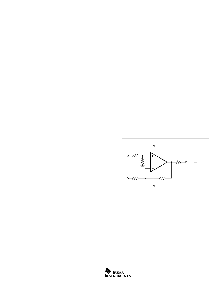
PIN CONFIGURATIONS
Top View
SO
Top View
SOT
1
2
3
4
8
7
6
5
NC
+V
S
Output
NC
NC
Inverting Input
Noninverting Input
≠V
S
1
2
3
5
4
+V
S
Inverting Input
Output
≠V
S
Noninverting Input
OAQI
1
2
3
5
4
Pin Orientation/Package Marking
NC = No Connection

OPA842
3
SBOS267A
www.ti.com
OPA842ID, OPA842IDBV
TYP
MIN/MAX OVER TEMPERATURE
0
∞
C to
≠40
∞
C to
MIN/
TEST
PARAMETER
CONDITIONS
+25
∞
C
+25
∞
C
(1)
70
∞
C
+85
∞
C
(2)
UNITS
MAX
LEVEL
(3 )
AC PERFORMANCE (see Figure 1)
Closed-Loop Bandwidth (V
O
= 100mVp-p)
G = +1, R
F
= 25
350
MHz
typ
C
G = +2
150
105
101
100
MHz
min
B
G = +5
45
30
29
29
MHz
min
B
G = +10
21
15
14
14
MHz
min
B
Gain-Bandwidth Product
200
136
135
135
MHz
min
B
Bandwidth for 0.1dB Gain Flatness
G = +2, R
L
= 100
, V
O
= 100mVp-p
56
MHz
typ
C
G = +1, R
L
= 100
, R
F
= 25
105
MHz
typ
C
Harmonic Distortion
G = +2, f = 5MHz, V
O
= 2Vp-p
2nd-Harmonic
R
L
= 100
≠80
≠78
≠77
≠76
dBc
max
B
R
L
= 500
≠94
≠92
≠91
≠90
dBc
max
B
3rd-Harmonic
R
L
= 100
≠97
≠96
≠95
≠94
dBc
max
B
R
L
=
500
≠93
≠91
≠90
≠90
dBc
max
B
2-Tone, 3rd-Order Intercept
G = +2, f = 10MHz
44
dBm
typ
C
Input Voltage Noise
f > 1MHz
2.6
2.8
3.0
3.1
nV/
Hz
max
B
Input Current Noise
f > 1MHz
2.7
2.8
2.9
3.0
pA/
Hz
max
B
Rise-and-Fall Time
0.2V Step
2.3
3.3
3.4
3.5
ns
max
B
Slew Rate
2V Step
400
300
250
225
V/
µ
s
min
B
Settling Time to 0.01%
2V Step
22
ns
typ
C
0.1%
2V Step
15
19.6
20.3
21.3
ns
max
B
1.0%
2V Step
9
10.2
11.3
12.5
ns
max
B
Differential Gain
G = +2, NTSC, R
L
= 150
0.003
%
typ
C
Differential Phase
G = +2, NTSC, R
L
= 150
0.008
deg
typ
C
DC PERFORMANCE
(4)
Open-Loop Voltage Gain (A
OL
)
V
O
= 0V
110
100
96
92
dB
min
A
Input Offset Voltage
V
CM
= 0V
±
0.30
±
1.2
±
1.4
±
1.5
mV
max
A
Average Offset Voltage Drift
V
CM
= 0V
±
4
±
4
µ
V/
∞
C
max
B
Input Bias Current
V
CM
= 0V
≠20
≠35
≠36
≠37
µ
A
max
A
Input Bias Current Drift
V
CM
= 0V
25
25
nA/
∞
C
max
B
Input Offset Current
V
CM
= 0V
±
0.35
±
1.0
±
1.15
±
1.17
µ
A
max
A
Input Offset Current Drift
V
CM
= 0V
±
2
±
2
nA/
∞
C
max
B
INPUT
Common-Mode Input Range (CMIR)
(5)
±
3.2
±
3.0
±
2.9
±
2.8
V
min
A
Common-Mode Rejection (CMRR)
V
CM
=
±
1V, Input Referred
95
85
84
82
dB
min
A
Input Impedance
Differential-Mode
V
CM
= 0V
14 || 1
k
|| pF
typ
C
Common-Mode
V
CM
= 0V
3.1 || 1.2
M
|| pF
typ
C
OUTPUT
Output Voltage Swing
R
L
> 1k
, Positive Output
3.2
3.0
±
2.9
±
2.8
V
min
A
R
L
> 1k
, Negative Output
≠3.7
≠3.5
≠3.4
≠3.3
V
min
A
R
L
= 100
, Positive Output
3.0
2.8
2.7
2.6
V
min
A
R
L
= 100
, Negative Output
≠3.5
≠3.3
≠3.2
≠3.1
V
min
A
Current Output, Sourcing
V
O
= 0V
±
100
±
90
±
85
±
80
mA
min
A
Closed-Loop Output Impedance
G = +2, f = 1kHz
0.00038
typ
C
POWER SUPPLY
Specified Operating Voltage
±
5
V
typ
C
Maximum Operating Voltage
±
6
±
6
±
6
V
min
A
Max Quiescent Current
V
S
=
±
5V
20.2
20.8
22.2
22.5
mA
max
A
Min Quiescent Current
V
S
=
±
5V
20.2
19.6
19.1
18.3
mA
min
A
Power-Supply Rejection Ratio
(+PSRR, ≠PSRR)
|V
S
| = 4.5V to 5.5V, Input Referred
100
90
88
85
dB
min
A
THERMAL CHARACTERISTICS
Specified Operating Range: D, DBV
≠40 to +85
∞
C
typ
C
Thermal Resistance,
JA
Junction-to-Ambient
D
SO-8
125
∞
C
typ
C
DBV
SOT23-5
150
∞
C
typ
C
ELECTRICAL CHARACTERISTICS: V
S
=
±
5V
Boldface limits are tested at +25
∞
C.
At T
A
= +25
∞
C, V
S
=
±
5V, R
F
= 402
, R
L
= 100
, and G = +2, unless otherwise noted. See Figure 1 for AC performance.
NOTES: (1) Junction temperature = ambient temperature for +25
∞
C min/max specifications. (2) Junction temperature = ambient at low temperature limit: junction
temperature = ambient +23
∞
C at high temperature limit for over temperature min/max specifications. (3) Test Levels: (A) 100% tested at +25
∞
C. Over-temperature
limits by characterization and simulation. (B) Limits set by characterization and simulation. (C) Typical value only for information. (4) Current is considered positive out-
of-node. V
CM
is the input common-mode voltage. (5) Tested < 3dB below minimum specified CMRR at
±
CMIR limits.

OPA842
4
SBOS267A
www.ti.com
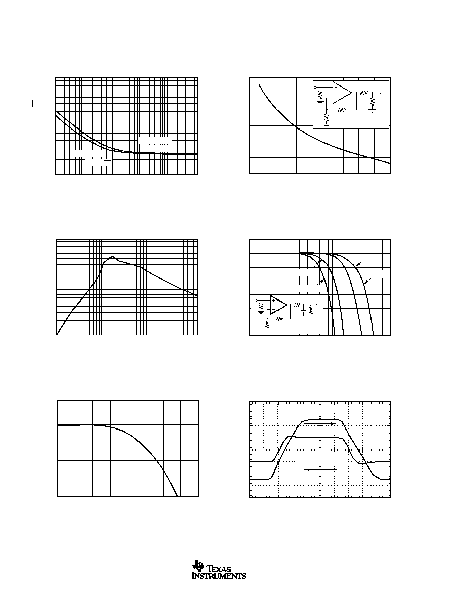
TYPICAL CHARACTERISTICS:
V
S
=
±
5V
At T
A
= 25
∞
C, G = +2, R
F
= 402
, and R
L
= 100
, unless otherwise noted.
NONINVERTING SMALL-SIGNAL
FREQUENCY RESPONSE
Frequency (MHz)
1
10
100
500
3
0
≠3
≠6
≠9
≠12
≠15
≠18
Normalized Gain (3dB/div)
V
O
= 0.1Vp-p
See Figure 1
G = +10
G = +1
R
F
= 25
G = +2
G = +5
INVERTING SMALL-SIGNAL
FREQUENCY RESPONSE
Frequency (MHz)
1
10
100
500
3
0
≠3
≠6
≠9
≠12
≠15
≠18
Normalized Gain (3dB/div)
R
G
= R
S
= 50
V
O
= 0.1Vp-p
R
F
Adjusted
See Figure 2
G = ≠10
G = ≠1
G = ≠2
G = ≠5
NONINVERTING LARGE-SIGNAL
FREQUENCY RESPONSE
Frequency (MHz)
1
10
100
500
9
6
3
0
≠3
≠6
≠9
≠12
Normalized Gain (3dB/div)
R
L
= 100
G = +2V/V
See Figure 1
0.1Vp-p
0.5Vp-p
1.0Vp-p
V
O
= 2Vp-p
V
O
= 5Vp-p
INVERTING LARGE-SCALE
FREQUENCY RESPONSE
Frequency (MHz)
1
10
100
500
9
6
3
0
≠3
≠6
≠9
≠12
≠15
≠18
Gain (3dB/div)
0.1Vp-p
1Vp-p
2Vp-p
5Vp-p
R
L
= 100
G = ≠2V/V
R
G
= 200
See Figure 2
NONINVERTING PULSE RESPONSE
Time (5ns/div)
Output V
oltage (100mV/div)
Output V
oltage (400mV/div)
200
100
0
≠100
≠200
1.2
0.8
0.4
0
≠0.4
≠0.8
≠1.2
G = +2
See Figure 1
Right Scale
Large Signal
±
1V
Small Signal
±
100mV
Left Scale
INVERTING PULSE RESPONSE
Time (5ns/div)
Output V
oltage (100mV/div)
Output V
oltage (400mV/div)
200
100
0
≠100
≠200
1.2
0.8
0.4
0
≠0.4
≠0.8
≠1.2
G = ≠2
R
G
= 200
See Figure 2
Right Scale
Large Signal
±
1V
Small Signal
±
100mV
Left Scale

OPA842
5
SBOS267A
www.ti.com
TYPICAL CHARACTERISTICS:
V
S
=
±
5V (Cont.)
At T
A
= 25
∞
C, G = +2, R
F
= 402
, and R
L
= 100
, unless otherwise noted.
5MHz HARMONIC DISTORTION vs LOAD RESISTANCE
Load Resistance (
)
Harmonic Distortion (dBc)
250
200
150
300
350
400
450
500
100
≠75
≠80
≠85
≠90
≠95
≠100
2nd-Harmonic
V
O
= 2Vp-p
See Figure 1
3rd-Harmonic
1MHz HARMONIC DISTORTION vs LOAD RESISTANCE
Load Resistance (
)
Harmonic Distortion (dBc)
250
200
150
300
350
400
450
500
100
≠85
≠90
≠95
≠100
≠105
≠110
V
O
= 2Vp-p
See Figure 1
2nd-Harmonic
3rd-Harmonic
HARMONIC DISTORTION vs FREQUENCY
Frequency (MHz)
0.5
1
10
20
≠60
≠70
≠80
≠90
≠100
≠110
Harmonic Distortion (dBc)
V
O
= 2Vp-p
R
L
= 200
G = +2
2nd-Harmonic
3rd-Harmonic
See Figure 1
HARMONIC DISTORTION vs OUTPUT VOLTAGE
Output Voltage Swing (Vp-p)
0.1
1
10
≠80
≠85
≠90
≠95
≠100
≠105
≠110
Harmonic Distortion (dBc)
R
L
= 200
F = 5MHz
2nd-Harmonic
3rd-Harmonic
See Figure 1
HARMONIC DISTORTION vs NONINVERTING GAIN
Noninverting Gain (V/V)
1
10
≠70
≠80
≠90
≠100
≠110
Harmonic Distortion (dBc)
V
O
= 2Vp-p
R
L
= 200
F = 5MHz
2nd-Harmonic
See Figure 1
3rd-Harmonic
HARMONIC DISTORTION vs INVERTING GAIN
Inverting Gain |V/V|
1
10
≠70
≠80
≠90
≠100
≠110
Harmonic Distortion (dBc)
See Figure 2
V
O
= 2Vp-p
R
L
= 200
F = 5MHz
R
F
= 402
2nd-Harmonic
3rd-Harmonic
OPA842
6
SBOS267A
www.ti.com
TYPICAL CHARACTERISTICS:
V
S
=
±
5V (Cont.)
At T
A
= 25
∞
C, G = +2, R
F
= 402
, and R
L
= 100
, unless otherwise noted.
INPUT VOLTAGE AND CURRENT NOISE
Frequency (Hz)
10
2
10
3
10
4
10
5
10
6
10
7
100
10
1
V
oltage Noise (nV
Hz)
Current Noise (pA
Hz)
Current Noise
Voltage Noise
2.7pA/
Hz
2.6nV/
Hz
2-TONE, 3RD-ORDER
INTERMODULATION INTERCEPT
Frequency (MHz)
Intercept Point (+dBm)
20
15
10
25
30
35
40
45
50
5
50
45
40
35
30
25
20
402
402
OPA842
50
50
50
P
I
P
O
RECOMMENDED R
S
vs CAPACITIVE LOAD
Capacitive Load (pF)
1
10
100
1k
100
10
1
R
S
(
)
FREQUENCY RESPONSE vs CAPACITIVE LOAD
Frequency (MHz)
10
100
500
3
0
≠3
≠6
≠9
≠12
≠15
≠18
Normalized Gain to Capacitive Load (dB)
C = 10pF
C = 22pF
C = 47pF
C = 100pF
R
S
50
1k
V
I
V
O
C
L
402
402
OPA842
GAIN = +1 FLATNESS
Frequency (25MHz/div)
0
25
50
200
75
100
125
150
175
0.2
0.1
0
≠0.1
≠0.2
≠0.3
≠0.4
≠0.5
≠0.6
Gain (0.1dB/div)
V
O
= 0.1Vp-p
R
F
= 25
R
L
= 100
PULSE RESPONSE G = +1
Time (2ns/div)
Output V
oltage (100mV/div)
Output V
oltage (400mV/div)
200
100
0
≠100
≠200
1.2
0.8
0.4
0
≠0.4
≠0.8
≠1.2
Right Scale
Large Signal
±
1V
Small Signal
Left Scale

OPA842
7
SBOS267A
www.ti.com
TYPICAL CHARACTERISTICS:
V
S
=
±
5V (Cont.)
At T
A
= 25
∞
C, G = +2, R
F
= 402
, and R
L
= 100
, unless otherwise noted.
CMRR AND PSRR vs FREQUENCY
Frequency (Hz)
10
1
10
2
10
3
10
4
10
5
10
6
10
7
10
8
Common-Mode Rejection Ratio (dB)
Power-Supply Rejection Ratio (dB)
120
100
80
60
40
20
0
≠PSRR
+PSRR
CMRR
OPEN-LOOP GAIN AND PHASE
Frequency (Hz)
10
1
10
2
10
3
10
4
10
5
10
6
10
7
10
8
10
9
Open-Loop Gain (dB)
Open-Loop Phase (
∞
)
120
100
80
60
40
20
0
≠20
0
≠30
≠60
≠90
≠120
≠150
≠180
≠210
20log (A
OL
)
A
OL
OUTPUT VOLTAGE AND CURRENT LIMITATIONS
I
O
(mA)
V
O
(V)
≠0.10
≠0.05
0
0.05
0.10
0.15
≠0.15
4
3
2
1
0
≠1
≠2
≠3
≠4
R
L
= 100
R
L
= 25
R
L
= 50
1W Internal
Power Limit
1W Internal
Power Limit
CLOSED-LOOP OUTPUT IMPEDANCE
vs FREQUENCY
Frequency (Hz)
10
2
10
3
10
4
10
5
10
6
10
7
10
8
Output Impedance (
)
10
1
0.1
0.01
0.001
0.0001
0.00001
NONINVERTING OVERDRIVE RECOVERY
Time (40ns/div)
Output V
oltage (2V/div)
Input V
oltage (1V/div)
8
6
4
2
0
≠2
≠4
≠6
≠8
4
3
2
1
0
≠1
≠2
≠3
≠4
Output
Left Scale
R
L
= 100
G = 2
See Figure 1
Input
Right Scale
INVERTING OVERDRIVE RECOVERY
Time (40ns/div)
Output V
oltage (2V/div)
Input V
oltage (1V/div)
8
6
4
2
0
≠2
≠4
≠6
≠8
4
3
2
1
0
≠1
≠2
≠3
≠4
Output
Left Scale
R
L
= 100
G = 2
See Figure 2
Input
Right Scale

OPA842
8
SBOS267A
www.ti.com
TYPICAL CHARACTERISTICS:
V
S
=
±
5V (Cont.)
At T
A
= 25
∞
C, G = +2, R
F
= 402
, and R
L
= 100
, unless otherwise noted.
SETTLING TIME
Time (ns)
Percent of Final V
alue (%)
15
10
5
20
25
30
35
40
45
50
0
0.250
0.200
0.150
0.100
0.050
0.000
≠0.050
≠0.100
≠0.150
≠0.200
≠0.250
V
O
= 2V step
R
L
= 100
G = 2
See Figure 1
VIDEO DIFFERENTIAL GAIN/DIFFERENTIAL PHASE
Video Loads
Dif
ferential Gain (%)
Dif
ferential Phase (
∞
)
2
3
4
5
1
0.008
0.006
0.004
0.002
0
0.08
0.06
0.04
0.02
0
G = 2
DG Negative Video
DP Negative
Video
DP Positive Video
DG Positive Video
TYPICAL DC DRIFT OVER TEMPERATURE
Ambient Temperature (
∞
C)
Input Of
fset V
oltage (mV)
Input Bias and Of
fset Current (
µ
A)
≠25
0
25
50
75
100
125
≠50
1
0.5
0
≠0.5
≠1
25
12.5
0
≠12.5
≠25
100x (Input Offset Current)
Right Scale
Input Offset Voltage
Left Scale
Input Bias Current
Right Scale
SUPPLY AND OUTPUT CURRENT vs TEMPERATURE
Ambient Temperature (
∞
C)
Output Current (5mA/div)
Supply Current (2mA/div)
≠25
0
25
50
75
100
125
≠50
120
115
110
105
100
95
90
85
80
24
22
20
18
16
14
12
10
8
Supply Current
Right Scale
Left Scale
Sink/Source Output Current
COMMON-MODE INPUT RANGE AND
OUTPUT SWING vs SUPPLY VOLTAGE
Supply Voltage (
±
V)
V
oltage Range (V)
±
4
±
5
±
6
±
3
6
4
2
0
≠2
≠4
≠6
±
Voltage Output
±
Voltage Input
COMMON-MODE AND
DIFFERENTIAL INPUT IMPEDANCE
Frequency (Hz)
10
2
10
3
10
4
10
5
10
6
10
7
10
8
10
9
Input Impedance (
)
10
7
10
6
10
5
10
4
10
3
10
2
Common-Mode Impedance
Differential Impedance

OPA842
9
SBOS267A
www.ti.com
TYPICAL CHARACTERISTICS:
V
S
=
±
5V (Cont.)
At T
A
= 25
∞
C, G = +2, R
F
= 402
, and R
L
= 100
, unless otherwise noted.
OPA842
OPA842
R
G
402
+5V
R
G
R
L
V
I
402
V
O
≠5V
+5V
≠5V
G
D =
402
R
G
DIFFERENTIAL SMALL-SIGNAL
FREQUENCY RESPONSE
Frequency (MHz)
1
10
100
500
3
0
≠3
≠6
≠9
≠12
≠15
≠18
Normalized Gain (dB)
G
D
= 5
G
D
= 10
G
D
= 1
G
D
= 2
DIFFERENTIAL LARGE-SIGNAL
FREQUENCY RESPONSE
Frequency (MHz)
10
100
500
9
6
3
0
≠3
≠6
≠9
≠12
Gain (dB)
0.2Vp-p
1Vp-p
2Vp-p
G
D
= 2
R
L
= 400
5Vp-p
8Vp-p
DIFFERENTIAL DISTORTION vs
LOAD RESISTANCE
Load Resistance (
)
Harmonic Distortion (dBc)
200
150
100
250
300
350
400
450
500
50
≠85
≠90
≠95
≠100
≠105
≠110
G = 2
F = 5MHz
V
O
= 4Vp-p
2nd-Harmonic
3rd-Harmonic
DIFFERENTIAL DISTORTION vs FREQUENCY
Frequency (MHz)
1
10
100
≠60
≠70
≠80
≠90
≠100
≠110
Harmonic Distortion (dBc)
R
L
= 400
V
O
= 4Vp-p
G
D
= 2
2nd-Harmonic
3rd-Harmonic
DIFFERENTIAL DISTORTION vs OUTPUT VOLTAGE
Output Voltage Swing (Vp-p)
1
10
≠80
≠85
≠90
≠95
≠100
≠105
≠110
≠115
Harmonic Distortion (dBc)
R
L
= 400
G
D
= 2
F = 5MHz
2nd-Harmonic
3rd-Harmonic
DIFFERENTIAL PERFORMANCE
TEST CIRCUIT

OPA842
10
SBOS267A
www.ti.com
APPLICATIONS INFORMATION
WIDEBAND VOLTAGE-FEEDBACK OPERATION
The OPA842's combination of speed and dynamic range is
easily achieved in a wide variety of application circuits,
providing that simple principles of good design practice are
observed. For example, good power-supply decoupling, as
shown in Figure 1, is essential to achieve the lowest possible
harmonic distortion and smooth frequency response.
Proper PC board layout and careful component selection will
maximize the performance of the OPA842 in all applications,
as discussed in the following sections of this data sheet.
Figure 1 shows the gain of +2 configuration used as the basis
for most of the typical characteristics. Most of the curves
were characterized using signal sources with 50
driving
impedance and with measurement equipment presenting
50
load impedance. In Figure 1, the 50
shunt resistor at
the V
I
terminal matches the source impedance of the test
generator while the 50
series resistor at the V
O
terminal
provides a matching resistor for the measurement equipment
load. Generally, data sheet specifications refer to the voltage
swing at the output pin (V
O
in Figure 1). The 100
load,
combined with the 804
total feedback network load, pre-
sents the OPA842 with an effective load of approximately
90
in Figure 1.
In the inverting case, just the feedback resistor appears as
part of the total output load in parallel with the actual load.
For the 100
load used in the typical characteristics, this
gives a total load of 80
in this inverting configuration. The
gain resistor is set to get the desired gain (in this case 200
for a gain of ≠2) while an additional input matching resistor
(R
M
) can be used to set the total input impedance equal to
the source if desired. In this case, R
M
= 66.5
in parallel with
the 200
gain setting resistor gives a matched input imped-
ance of 50
. This matching is only needed when the input
needs to be matched to a source impedance, as in the
characterization testing done using the circuit of Figure 2.
The OPA842 offers extremely good DC accuracy as well as
low noise and distortion. To take full advantage of that DC
precision, the total DC impedance looking out of each of the
input nodes must be matched to get bias current cancella-
tion. For the circuit of Figure 2, this requires the 147
resistor
shown to ground on the noninverting input. The calculation
for this resistor includes a DC-coupled 50
source imped-
ance along with R
G
and R
M
. Although this resistor will provide
cancellation for the bias current, it must be well decoupled
(0.1
µ
F in Figure 2) to filter the noise contribution of the
resistor and the input current noise.
As the required R
G
resistor approaches 50
at higher gains,
the bandwidth for the circuit in Figure 2 will far exceed the
bandwidth at that same gain magnitude for the noninverting
circuit of Figure 1. This occurs due to the lower "noise gain"
for the circuit of Figure 2 when the 50
source impedance is
included in the analysis. For instance, at a signal gain of ≠8
(R
G
= 50
, R
M
= open, R
F
= 402
) the noise gain for the
circuit of Figure 2 will be 1 + 402
/(50
+ 50
) = 5 due to
the addition of the 50
source in the noise gain equation.
This gives considerable higher bandwidth than the
noninverting gain of +8. Using the 200MHz gain bandwidth
product for the OPA842, an inverting gain of ≠8 from a 50
source to a 50
R
G
will give approximately 40MHz band-
width, whereas the noninverting gain of +8 will give 25MHz.
FIGURE 1. Gain of +2. High-frequency application and
characterization circuit.
OPA842
+5V
≠5V
≠V
S
+V
S
R
S
50
V
O
V
IN
50
+
2.2
µ
F
+
2.2
µ
F
0.1
µ
F
R
G
402
R
F
402
50
Source
50
Load
0.1
µ
F
WIDEBAND INVERTING OPERATION
Operating the OPA842 as an inverting amplifier has several
benefits and is particularly useful when a matched 50
source and input impedance is required. Figure 2 shows the
inverting gain of ≠2 circuit used as the basis of the inverting
mode typical characteristics.
FIGURE 2. Inverting G = ≠2 Specifications and Test Circuit.
OPA843
+5V
≠5V
50
V
O
V
I
+
0.1
µ
F
2.2
µ
F
+
0.1
µ
F
2.2
µ
F
R
M
66.5
R
T
147
R
F
402
50
Source
50
Load
0.1
µ
F
R
G
200
OPA842
11
SBOS267A
www.ti.com
BUFFERING HIGH-PERFORMANCE ADCs
To achieve full performance from a high dynamic range ADC,
considerable care must be exercised in the design of the input
amplifier interface circuit. The example circuit on the front
page shows a typical AC-coupled interface to a very high
dynamic range converter. This AC coupled example allows
the OPA842 to be operated using a signal range that swings
symmetrically around ground (0V). The 2Vp-p swing is then
level-shifted through the blocking capacitor to a midscale
reference level, which is created by a well-decoupled resistive
divider off the converter's internal reference voltages. To
have a negligible effect on the rated Spurious-Free Dynamic
Range (SFDR) of the converter, the amplifier's SFDR should
be at least 10dB greater than the converter. The OPA842 has
no effect on the rated distortion of the ADS850, given its 82dB
SFDR at 2Vp-p, 5MHz. The > 92dB SFDR for the OPA842 in
this configuration will not degrade the converter.
Successful application of the OPA842 for ADC driving re-
quires careful selection of the series resistor at the amplifier
output, along with the additional shunt capacitor at the ADC
input. To some extent, selection of this RC network will be
determined empirically for each model of the converter. Many
high-performance CMOS ADCs, like the ADS850, perform
better with the shunt capacitor at the input pin. This capacitor
provides low source impedance for the transient currents
produced by the sampling process. Improved SFDR is often
obtained by adding this external capacitor, whose value is
often recommended in this converter data sheet. The exter-
nal capacitor, in combination with the built-in capacitance of
the ADC input, presents a significant capacitive load to the
OPA842. Without a series isolation resistor, an undesirable
peaking or loss of stability in the amplifier may result.
Since the DC bias current of the CMOS ADC input is
negligible, the resistor has no effect on overall gain or offset
accuracy. Refer to the typical characteristic "R
S
vs Capacitive
Load" to obtain a good starting value for the series resistor.
This will ensure flat frequency response to the ADC input.
Increasing the external capacitor value will allow the series
resistor to be reduced. Intentionally bandlimiting using this
RC network can also be used to limit noise at the converter
input.
VIDEO LINE DRIVING
Most video distribution systems are designed with 75
series
resistors to drive a matched 75
cable. In order to deliver a
net gain of 1 to the 75
matched load, the amplifier is
typically set up for a voltage gain of +2, compensating for the
6dB attenuation of the voltage divider formed by the series
and shunt 75
resistors at either end of the cable.
The circuit of Figure 1 applies to this requirement if all
references to 50
resistors are replaced by 75
values.
Often, the amplifier gain is further increased to 2.2, which
recovers the additional DC loss of a typical long cable run. This
change would require the gain resistor (R
G
) in Figure 1 to be
reduced from 402
to 335
. In either case, both the gain
flatness and the differential gain/phase performance of the
OPA842 will provide exceptional results in video distribution
applications. Differential gain and phase measure the change
in overall small-signal gain and phase for the color sub-carrier
frequency (3.58MHz in NTSC systems) versus changes in the
large-signal output level (which represents luminance informa-
tion in a composite video signal). The OPA842, with the typical
150
load of a single matched video cable, shows less than
0.01%/0.01
∞
differential gain/phase errors over the standard
luminance range for a positive video (negative sync) signal.
Similar performance would be observed for negative video
signals.
SINGLE OP AMP DIFFERENTIAL AMPLIFIER
The voltage-feedback architecture of the OPA842, with its
high Common-Mode Rejection Ratio (CMRR), will provide
exceptional performance in differential amplifier configura-
tions. Figure 3 shows a typical configuration. The starting
point for this design is the selection of the R
F
value in the
range of 200
to 2k
. Lower values reduce the required R
G
,
increasing the load on the V
2
source and on the OPA842
output. Higher values increase output noise and exacerbate
the effects of parasitic board and device capacitances. Fol-
lowing the selection of R
F
, R
G
must be set to achieve the
desired inverting gain for V
2
. Remember that the bandwidth
will be set approximately by the Gain Bandwidth Product
(GBP) divided by the noise gain (1 + R
F
/R
G
). For accurate
differential operation (i.e., good CMRR), the ratio R
2
/R
1
must
be set equal to R
F
/R
G
.
FIGURE 3. High-Speed, Single Differential Amplifier.
OPA842
+5V
≠5V
R
2
50
Power-supply decoupling not shown.
V
2
R
1
V
1
R
F
R
G
V
O
=
(V
1
≠ V
2
)
R
F
R
G
when
=
R
2
R
1
R
F
R
G
Usually, it is best to set the absolute values of R
2
and R
1
equal to R
F
and R
G
, respectively; this equalizes the divider
resistances and cancels the effect of input bias currents.
However, it is sometimes useful to scale the values of R
2
and
R
1
in order to adjust the loading on the driving source V
1
. In
most cases, the achievable low-frequency CMRR will be
limited by the accuracy of the resistor values. The 85dB
CMRR of the OPA842 itself will not determine the overall
circuit CMRR unless the resistor ratios are matched to better
than 0.003%. If it is necessary to trim the CMRR, then R
2
is
the suggested adjustment point.

OPA842
12
SBOS267A
www.ti.com
THREE OP AMP DIFFERENCING
(Instrumentation Topology)
The primary drawback of the single op amp differential
amplifier is its relatively low input impedances. Where high
impedance is required at the differential input, a standard
instrumentation amplifier (INA) topology may be built using
the OPA842 as the differencing stage. Figure 4 shows an
example of this, in which the two input amplifiers are pack-
aged together as a dual voltage-feedback op amp, the
OPA2822. This approach saves board space, cost, and
power compared to using two additional OPA842 devices,
and still achieves very good noise and distortion perfor-
mance due to the moderate loading on the input amplifiers.
requires its outputs terminated to a compliance voltage other
than ground for operation, then the appropriate voltage level
may be applied to the noninverting input of the OPA842.
FIGURE 4. Wideband 3-Op Amp Differencing Amplifier.
OPA842
Power-supply decoupling not shown.
V
O
V
1
R
G
500
V
2
OPA2822
+5V
+5V
≠5V
≠5V
OPA2822
500
500
R
F1
500
500
500
R
F1
500
In this circuit, the common-mode gain to the output is always
1, due to the four matched 500
resistors, whereas the
differential gain is set by (1 + 2R
F1
/R
G
), which is equal to 2
using the values in Figure 4. The differential to single-ended
conversion is still performed by the OPA842 output stage.
The high-impedance inputs allow the V
1
and V
2
sources to be
terminated or impedance matched as required. If the V
1
and
V
2
inputs are already truly differential, such as the output
from a signal transformer, then a single matching termination
resistor may be used between them. Remember, however,
that a defined DC signal path must always exist for the V
1
and V
2
inputs; for the transformer case, a center-tapped
secondary connected to ground would provide an optimum
DC operating point.
DAC TRANSIMPEDANCE AMPLIFIER
High-frequency Digital-to-Analog Converters (DACs) require
a low-distortion output amplifier to retain their SFDR perfor-
mance into real-world loads. A single-ended output drive
implementation is shown in Figure 5. In this circuit, only one
side of the complementary output drive signal is used. The
diagram shows the signal output current connected into the
virtual ground-summing junction of the OPA842, which is set
up as a transimpedance stage or "I-V converter." The unused
current output of the DAC is connected to ground. If the DAC
FIGURE 5. Wideband Low-Distortion DAC Transimpedance
Amplifier.
OPA842
High-Speed
DAC
V
O
= I
D
R
F
R
F
C
F
GBP
Gain Bandwidth
Product (Hz) for the OPA842
C
D
I
D
I
D
The DC gain for this circuit is equal to R
F
. At high frequen-
cies, the DAC output capacitance will produce a zero in the
noise gain for the OPA842 that may cause peaking in the
closed-loop frequency response. C
F
is added across R
F
to
compensate for this noise-gain peaking. To achieve a flat
transimpedance frequency response, this pole in the feed-
back network should be set to:
1
2
4
R C
GBP
R C
F
F
F
D
=
(1)
which will give a corner frequency f
≠3dB
of approximately:
f
GBP
R C
dB
F
D
-
=
3
2
(2)
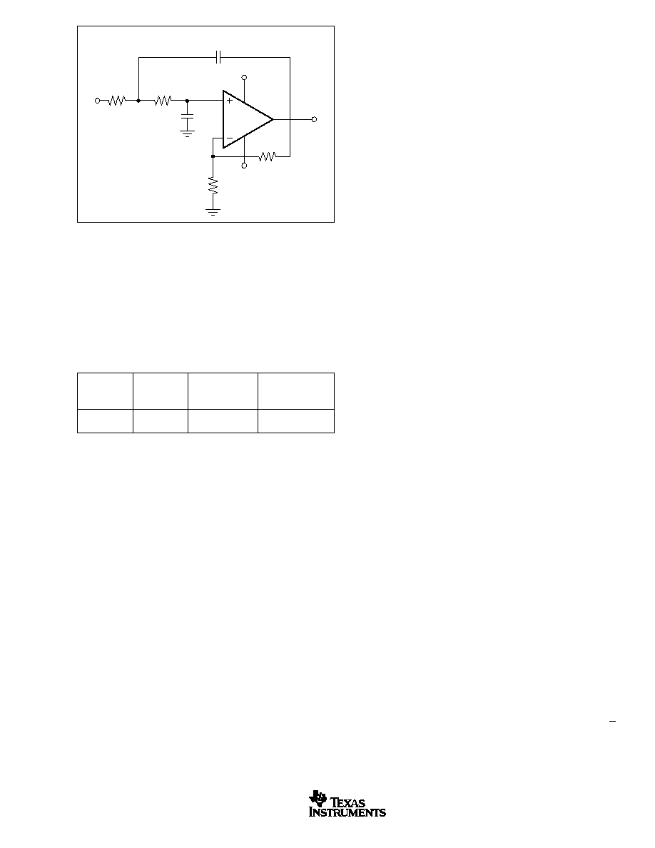
ACTIVE FILTERS
Most active filter topologies will have exceptional performance
using the broad bandwidth and unity-gain stability of the
OPA842. Topologies employing capacitive feedback require a
unity-gain stable, voltage-feedback op amp. Sallen-Key filters
simply use the op amp as a noninverting gain stage inside an
RC network. Either current- or voltage-feedback op amps may
be used in Sallen-Key implementations.
See Figure 6 for an example Sallen-Key low-pass filter, in
which the OPA842 is set up to deliver a low-frequency gain of
+2. The filter component values have been selected to achieve
a maximally flat Butterworth response with a 5MHz, ≠3dB
bandwidth. The resistor values have been slightly adjusted to
compensate for the effects of the 150MHz bandwidth provided
by the OPA842 in this configuration. This filter may be com-
bined with the ADC driver suggestions to provide moderate (2-
pole) Nyquist filtering, limiting noise, and out-of-band harmon-
ics into the input of an ADC. This filter will deliver the
exceptionally low harmonic distortion required by high SFDR
ADCs such as the ADS850 (14-bit, 10MSPS, 82dB SFDR).
OPA842
13
SBOS267A
www.ti.com
DESIGN-IN TOOLS
DEMONSTRATION BOARDS
Two PC boards are available to assist in the initial evaluation
of circuit performance using the OPA842 in its two package
styles. Both of these are available, free, as an unpopulated PC
board delivered with descriptive documentation. The summary
information for these boards is shown in the table below.
and parasitic capacitance considerations. For a noninverting
unity-gain follower application, the feedback connection should
be made with a 25
resistor--not a direct short. This will
isolate the inverting input capacitance from the output pin
and improve the frequency response flatness. Usually, the
feedback resistor value should be between 200
and 1k
.
Below 200
, the feedback network will present additional
output loading which can degrade the harmonic distortion
performance of the OPA842. Above 1k
, the typical parasitic
capacitance (approximately 0.2pF) across the feedback re-
sistor may cause unintentional band limiting in the amplifier
response.
A good rule of thumb is to target the parallel combination of R
F
and R
G
(see Figure 1) to be less than about 200
. The
combined impedance R
F
|| R
G
interacts with the inverting input
capacitance, placing an additional pole in the feedback net-
work, and thus a zero in the forward response. Assuming a 2pF
total parasitic on the inverting node, holding R
F
|| R
G
< 200
will keep this pole above 400MHz. By itself, this constraint
implies that the feedback resistor R
F
can increase to several
k
at high gains. This is acceptable as long as the pole formed
by R
F
and any parasitic capacitance appearing in parallel is
kept out of the frequency range of interest.
In the inverting configuration, an additional design consider-
ation must be noted. R
G
becomes the input resistor and
therefore the load impedance to the driving source. If imped-
ance matching is desired, R
G
may be set equal to the
required termination value. However, at low inverting gains,
the resultant feedback resistor value can present a signifi-
cant load to the amplifier output. For example, an inverting
gain of 2 with a 50
input matching resistor (= R
G
) would
require a 100
feedback resistor, which would contribute to
output loading in parallel with the external load. In such a
case, it would be preferable to increase both the R
F
and R
G
values, and then achieve the input matching impedance with
a third resistor to ground (see Figure 2). The total input
impedance becomes the parallel combination of R
G
and the
additional shunt resistor.
BANDWIDTH vs GAIN
Voltage-feedback op amps exhibit decreasing closed-loop
bandwidth as the signal gain is increased. In theory, this
relationship is described by the GBP shown in the specifica-
tions. Ideally, dividing GBP by the noninverting signal gain
(also called the Noise Gain, or NG) will predict the closed-
loop bandwidth. In practice, this only holds true when the
phase margin approaches 90
∞
, as it does in high-gain con-
figurations. At low signal gains, most amplifiers will exhibit a
more complex response with lower phase margin. The
OPA842 is optimized to give a maximally flat 2nd-order
Butterworth response in a gain of 2. In this configuration, the
OPA842 has approximately 60
∞
of phase margin and will
show a typical ≠3dB bandwidth of 150MHz. When the phase
margin is 60
∞
, the closed-loop bandwidth is approximately
2
greater than the value predicted by dividing GBP by the noise
gain. Increasing the gain will cause the phase margin to
approach 90
∞
and the bandwidth to more closely approach
the predicted value of (GBP/NG). At a gain of +10, the
FIGURE 6. 5MHz Butterwoth Low-Pass Active Filter.
OPA842
+5V
≠5V
R
2
505
C
1
150pF
R
1
124
V
O
V
1
R
G
402
R
F
402
C
2
100pF
Power-supply
decoupling not shown.
Go to the TI web site (www.ti.com) to request evaluation
boards in the OPA842 product folder.
MACROMODELS AND APPLICATIONS SUPPORT
Computer simulation of circuit performance using SPICE is
often a quick way to analyze the performance of the OPA842
and its circuit designs. This is particularly true for video and RF
amplifier circuits where parasitic capacitance and inductance
can play a major role on circuit performance. A SPICE model
for the OPA842 is available through the TI web page
(www.ti.com). The applications department is also available
for design assistance. These models predict typical small-
signal AC, transient steps, DC performance, and noise under
a wide variety of operating conditions. The models include the
noise terms found in the electrical specifications of the data
sheet. These models do not attempt to distinguish between
the package types in their small-signal AC performance.
OPERATING SUGGESTIONS
OPTIMIZING RESISTOR VALUES
Since the OPA842 is a unity-gain stable, voltage-feedback
op amp, a wide range of resistor values may be used for the
feedback and gain setting resistors. The primary limits on
these values are set by dynamic range (noise and distortion)
LITERATURE
BOARD
REQUEST
PRODUCT
PACKAGE
PART NUMBER
NUMBER
OPA842ID
SO-8
DEM-OPA68xU
SBOU010
OPA842IDBV
SOT23-5
DEM-OPA6xxN
SBOU009

OPA842
14
SBOS267A
www.ti.com
21MHz bandwidth shown in the Electrical Characteristics
agrees with that predicted using the simple formula and the
typical GBP of 200MHz.
OUTPUT DRIVE CAPABILITY
The OPA842 has been optimized to drive the demanding load
of a doubly-terminated transmission line. When a 50
line is
driven, a series 50
into the cable and a terminating 50
load
at the end of the cable are used. Under these conditions, the
cable's impedance will appear resistive over a wide frequency
range, and the total effective load on the OPA842 is 100
in
parallel with the resistance of the feedback network. The
electrical characteristics show a +2.8V/≠3.3V swing into this
load--which will then be reduced to a +1.4V/≠1.65V swing at
the termination resistor. The
±
90mA output drive over tem-
perature provides adequate current drive margin for this load.
Higher voltage swings (and lower distortion) are achievable
when driving higher impedance loads.
A single video load typically appears as a 150
load (using
standard 75
cables) to the driving amplifier. The OPA842
provides adequate voltage and current drive to support up to
three parallel video loads (50
total load) for an NTSC
signal. With only one load, the OPA842 achieves an excep-
tionally low 0.003%/0.008
∞
dG/dP error.
DRIVING CAPACITIVE LOADS
One of the most demanding, and yet very common, load
conditions for an op amp is capacitive loading. A high-speed,
high open-loop gain amplifier like the OPA842 can be very
susceptible to decreased stability and closed-loop response
peaking when a capacitive load is placed directly on the
output pin. In simple terms, the capacitive load reacts with
the open-loop output resistance of the amplifier to introduce
an additional pole into the loop and thereby decrease the
phase margin. This issue has become a popular topic of
application notes and articles, and several external solutions
to this problem have been suggested. When the primary
considerations are frequency response flatness, pulse re-
sponse fidelity, and/or distortion, the simplest and most
effective solution is to isolate the capacitive load from the
feedback loop by inserting a series isolation resistor between
the amplifier output and the capacitive load. This does not
eliminate the pole from the loop response, but rather shifts it
and adds a zero at a higher frequency. The additional zero
acts to cancel the phase lag from the capacitive load pole,
thus increasing the phase margin and improving stability.
The Typical Characteristics show the recommended "R
S
vs
Capacitive Load" and the resulting frequency response at the
load. The criterion for setting the recommended resistor is
maximum bandwidth, flat frequency response at the load.
Since there is now a passive low-pass filter between the
output pin and the load capacitance, the response at the
output pin itself is typically somewhat peaked, and becomes
flat after the roll-off action of the RC network. This is not a
concern in most applications, but can cause clipping if the
desired signal swing at the load is very close to the amplifier's
swing limit. Such clipping would be most likely to occur in
pulse response applications where the frequency peaking is
manifested as an overshoot in the step response.
Parasitic capacitive loads greater than 2pF can begin to
degrade the performance of the OPA842. Long PC board
traces, unmatched cables, and connections to multiple de-
vices can easily cause this value to be exceeded. Always
consider this effect carefully, and add the recommended
series resistor as close as possible to the OPA842 output pin
(see Board Layout section).
DISTORTION PERFORMANCE
The OPA842 is capable of delivering an exceptionally low
distortion signal at high frequencies and low gains. The
distortion plots in the Typical Characteristics show the typical
distortion under a wide variety of conditions. Most of these
plots are limited to 100dB dynamic range. The OPA842's
distortion does not rise above ≠100dBc until either the signal
level exceeds 0.5V and/or the fundamental frequency ex-
ceeds 500kHz. Distortion in the audio band is
≠120dBc.
Generally, until the fundamental signal reaches very high
frequencies or powers, the 2nd-harmonic will dominate the
distortion with a negligible 3rd-harmonic component. Focus-
ing then on the 2nd-harmonic, increasing the load imped-
ance improves distortion directly. Remember that the total
load includes the feedback network--in the noninverting
configuration this is the sum of R
F
+ R
G
, whereas in the
inverting configuration this is just R
F
(see Figure 1). Increas-
ing the output voltage swing increases harmonic distortion
directly. Increasing the signal gain will also increase the 2nd-
harmonic distortion. Again, a 6dB increase in gain will in-
crease the 2nd- and 3rd-harmonic by 6dB even with a
constant output power and frequency. Finally, the distortion
increases as the fundamental frequency increases due to the
roll off in the loop gain with frequency. Conversely, the
distortion will improve going to lower frequencies down to the
dominant open-loop pole at approximately 600Hz. Starting
from the ≠100dBc 2nd-harmonic for 2Vp-p into 200
, G = +2
distortion at 1MHz (from the Typical Characteristics), the
2nd-harmonic distortion at 20kHz should be approximately:
≠100dB ≠ 20log (1MHz/20kHz) = ≠134dBc
The OPA842 has an extremely low 3rd-order harmonic distor-
tion. This also gives an exceptionally good 2-tone, 3rd-order
intermodulation intercept, as shown in the Typical Character-
istics. This intercept curve is defined at the 50
load when
driven through a 50
-matching resistor to allow direct com-
parisons to RF MMIC devices. This network attenuates the
voltage swing from the output pin to the load by 6dB. If the
OPA842 drives directly into the input of a high-impedance
device, such as an ADC, this 6dB attenuation is not taken.
Under these conditions, the intercept will increase by a mini-
mum 6dBm. The intercept is used to predict the intermodulation
spurious for two closely spaced frequencies. If the two test
frequencies, f
1
and f
2
, are specified in terms of average and
delta frequency, f
O
= (f
1
+ f
2
)/2 and
f = |f
2
≠ f
1
|/2, the two 3rd-
order, close-in spurious tones will appear at f
O
±
(3 ∑
f). The
difference between the two equal test-tone power levels and
these intermodulation spurious power levels is given by

OPA842
15
SBOS267A
www.ti.com
2 ∑ (IM3 ≠ P
O
), where IM3 is the intercept taken from the typical
characteristic curve and P
O
is the power level in dBm at the
50
load for one of the two closely spaced test frequencies.
For instance, at 10MHz the OPA842 at a gain of +2 has an
intercept of 45dBm at a matched 50
load. If the full envelope
of the two frequencies needs to be 2Vp-p, this requires each
tone to be 4dBm. The 3rd-order intermodulation spurious
tones will then be 2 ∑ (45 ≠ 4) = 82dBc below the test-tone
power level (≠80dBm). If this same 2Vp-p 2-tone envelope
were delivered directly into the input of an ADC without the
matching loss or loading of the 50
network, the intercept
would increase to at least 51dBm. With the same signal and
gain conditions driving directly into a light load, the spurious
tones will then be at least 2 ∑ (51 ≠ 4) = 94dBc below the
1Vp-p test-tone signal levels.
NOISE PERFORMANCE
The OPA842 complements its ultra low harmonic distortion
with low input noise terms. Both the input-referred voltage
noise and the two input-referred current noise terms combine
to give a low output noise under a wide variety of operating
conditions. Figure 7 shows the op amp noise analysis model
E
E
I
R
kTR
I R
NG
kTR
NG
N
NI
BN
S
S
BI
F
F
=
+
(
)
+
+
+
2
2
2
4
4
(4)
Evaluating these two equations for the OPA842 circuit pre-
sented in Figure 1 will give a total output spot noise voltage
of 6.6nV/
Hz and an equivalent input spot noise voltage of
3.3nV/
Hz.
Narrow band communications systems are more commonly
concerned with the noise figure for the amplifier. The total
input referred voltage noise expression (see Equation 4),
may be used to calculate the noise figure. Equation 5 shows
this noise figure expression using the NG of Equation 4 for
the noninverting configuration where the input terminating
resistor, R
T
, has been set to match the source impedance,
R
S
(see Figure 1).
NF
E
kTR
N
S
kT
E
J at
K
=
+
=
-
∞
10
2
2
4
21
290
log
(5)
Evaluating Equation 5 for the circuit of Figure 1 gives a noise
figure = 17.6dB.
DC OFFSET CONTROL
The OPA842 can provide excellent DC signal accuracy due to
its high open-loop gain, high common-mode rejection, high
power-supply rejection, and low input offset voltage and bias
current offset errors. To take full advantage of this low input
offset voltage, careful attention to input bias current cancella-
tion is also required. The high-speed input stage for the
OPA842 has a relatively high input bias current (20
µ
A typ into
the pins) but with a very close match between the two input
currents--typically 0.35
µ
A input offset current. The total out-
put offset voltage may be considerably reduced by matching
the source impedances looking out of the two inputs. For
example, one way to add bias current cancellation to the
circuit of Figure 1 would be to insert a 175
series resistor into
the noninverting input from the 50
terminating resistor. When
the 50
source resistor is DC-coupled, this will increase the
source impedance for the noninverting input bias current to
200
. Since this is now equal to the impedance looking out of
the inverting input (R
F
|| R
G
), the circuit will cancel the gains
for the bias currents to the output leaving only the offset
current times the feedback resistor as a residual DC error term
at the output. Using a 402
feedback resistor, this output error
will now be less than 1
µ
A ∑ 402
= 0.4mV at 25
∞
C.
THERMAL ANALYSIS
The OPA842 will not require heat sinking or airflow in most
applications. Maximum desired junction temperature would
set the maximum allowed internal power dissipation as
described below. In no case should the maximum junction
temperature be allowed to exceed +175
∞
C.
Operating junction temperature (T
J
) is given by T
A
+ P
D
∑
JA
.
The total internal power dissipation (P
D
) is the sum of quies-
cent power (P
DQ
) and additional power dissipated in the
output stage (P
DL
) to deliver load power. Quiescent power is
FIGURE 7. Op Amp Noise Analysis Model.
4kT
R
G
R
G
R
F
R
S
OPA842
I
BI
E
O
I
BN
4kT = 1.6E ≠ 20J
at 290
∞
K
E
RS
E
NI
4kTR
S
4kTR
F
with all the noise terms included. In this model, all the noise
terms are taken to be noise voltage or current density terms
in either nV/
Hz or pA/
Hz.
The total output spot noise voltage is computed as the
square root of the squared contributing terms to the output
noise voltage. This computation is adding all the contributing
noise powers at the output by superposition, then taking the
square root to get back to a spot noise voltage. Equation 3
shows the general form for this output noise voltage using
the terms presented in Figure 7.
E
E
I
R
kTR NG
I R
kTR NG
O
NI
BN
S
S
BI
F
F
=
+
(
)
+
+
(
)
+
2
2
2
2
4
4
(3)
Dividing this expression by the noise gain (NG = 1 + R
F
/R
G
)
will give the equivalent input referred spot noise voltage at
the noninverting input, as shown in Equation 4.

OPA842
16
SBOS267A
www.ti.com
simply the specified no-load supply current times the total
supply voltage across the part. P
DL
will depend on the
required output signal and load but would, for a grounded
resistive load, be at a maximum when the output is fixed at a
voltage equal to 1/2 of either supply voltage (for equal bipolar
supplies). Under this worst-case condition, P
DL
= V
S
2
/(4 ∑ R
L
),
where R
L
includes feedback network loading.
Note that it is the power in the output stage and not in the
load that determines internal power dissipation.
As a worst-case example, compute the maximum T
J
using an
OPA842IDBV (SOT23-5 package) in the circuit of Figure 1
operating at the maximum specified ambient temperature of
+85
∞
C.
P
D
= 10V(22.5mA) + 5
2
/(4 ∑ (100
|| 800
)) = 291mW
Maximum T
J
= +85
∞
C + (0.29W ∑ 150
∞
C/W) = 129
∞
C
BOARD LAYOUT
Achieving optimum performance with a high-frequency am-
plifier such as the OPA842 requires careful attention to board
layout parasitics and external component types. Recommen-
dations that will optimize performance include:
a) Minimize parasitic capacitance to any AC ground for
all of the signal I/O pins. Parasitic capacitance on the
output and inverting input pins can cause instability: on the
noninverting input, it can react with the source impedance to
cause unintentional bandlimiting. To reduce unwanted ca-
pacitance, a window around the signal I/O pins should be
opened in all of the ground and power planes around those
pins. Otherwise, ground and power planes should be unbro-
ken elsewhere on the board.
b) Minimize the distance (< 0.25") from the power-supply
pins to high-frequency 0.1
µ
F decoupling capacitors. At
the device pins, the ground and power-plane layout should
not be in close proximity to the signal I/O pins. Avoid narrow
power and ground traces to minimize inductance between
the pins and the decoupling capacitors. The power-supply
connections should always be decoupled with these capaci-
tors. Larger (2.2
µ
F to 6.8
µ
F) decoupling capacitors, effective
at lower frequency, should also be used on the main supply
pins. These may be placed somewhat farther from the device
and may be shared among several devices in the same area
of the PC board.
c) Careful selection and placement of external compo-
nents will preserve the high-frequency performance of the
OPA842. Resistors should be a very low reactance type.
Surface-mount resistors work best and allow a tighter overall
layout. Metal-film and carbon composition, axially leaded
resistors can also provide good high-frequency performance.
Again, keep their leads and PC board trace length as short as
possible. Never use wire-wound type resistors in a high-
frequency application. Since the output pin and inverting input
pin are the most sensitive to parasitic capacitance, always
position the feedback and series output resistor, if any, as
close as possible to the output pin. Other network compo-
nents, such as noninverting input termination resistors, should
also be placed close to the package. Where double-side
component mounting is allowed, place the feedback resistor
directly under the package on the other side of the board
between the output and inverting input pins. Even with a low
parasitic capacitance shunting the external resistors, exces-
sively high resistor values can create significant time con-
stants that can degrade performance. Good axial metal-film or
surface-mount resistors have approximately 0.2pF in shunt
with the resistor. For resistor values > 1.5k
, this parasitic
capacitance can add a pole and/or a zero below 500MHz that
can effect circuit operation. Keep resistor values as low as
possible consistent with load-driving considerations. It has
been suggested here that a good starting point for design
would be to set R
G
|| R
F
200
. Doing this will automatically
keep the resistor noise terms low, and minimize the effect of
their parasitic capacitance.
d) Connections to other wideband devices on the board
may be made with short direct traces or through onboard
transmission lines. For short connections, consider the
trace and the input to the next device as a lumped capacitive
load. Relatively wide traces (50mils to 100mils) should be
used, preferably with ground and power planes opened up
around them. Estimate the total capacitive load and set R
S
from the plot of "Recommended R
S
vs Capacitive Load." Low
parasitic capacitive loads (< 5pF) may not need an R
S
since
the OPA842 is nominally compensated to operate with a 2pF
parasitic load. Higher parasitic capacitive loads without an R
S
are allowed as the signal gain increases (increasing the
unloaded phase margin). If a long trace is required, and the
6dB signal loss intrinsic to a doubly-terminated transmission
line is acceptable, implement a matched impedance trans-
mission line using microstrip or stripline techniques (consult
an ECL design handbook for microstrip and stripline layout
techniques). A 50
environment is normally not necessary
on board, and in fact, a higher impedance environment will
improve distortion as shown in the distortion versus load
plots. With a characteristic board trace impedance defined
based on board material and trace dimensions, a matching
series resistor into the trace from the output of the OPA842
is used as well as a terminating shunt resistor at the input of
the destination device. Remember also that the terminating
impedance will be the parallel combination of the shunt
resistor and input impedance of the destination device; this
total effective impedance should be set to match the trace
impedance. If the 6dB attenuation of a doubly-terminated
transmission line is unacceptable, a long trace can be series-
terminated at the source end only. Treat the trace as a
capacitive load in this case and set the series resistor value
as shown in the plot of "R
S
vs Capacitive Load." This will not
preserve signal integrity as well as a doubly-terminated line.
If the input impedance of the destination device is low, there
will be some signal attenuation due to the voltage divider
formed by the series output into the terminating impedance.
e) Socketing a high-speed part like the OPA842 is not
recommended. The additional lead length and pin-to-pin
capacitance introduced by the socket can create an ex-
tremely troublesome parasitic network, which can make it

OPA842
17
SBOS267A
www.ti.com
almost impossible to achieve a smooth, stable frequency
response. Best results are obtained by soldering the OPA842
onto the board.
INPUT AND ESD PROTECTION
The OPA842 is built using a very high-speed complementary
bipolar process. The internal junction breakdown voltages are
FIGURE 8. Internal ESD Protection.
External
Pin
+V
CC
≠V
CC
relatively low for these very small geometry devices. These
breakdowns are reflected in the Absolute Maximum Ratings
table. All device pins are protected with internal ESD protec-
tion diodes to the power supplies, as shown in Figure 8.
These diodes provide moderate protection to input overdrive
voltages above the supplies as well. The protection diodes
can typically support 30mA continuous current. Where higher
FIGURE 9. Gain of +2 with Input Protection.
OPA842
+5V
≠5V
50
50
Power-supply
decoupling not shown.
174
D1
D2
V
1
301
R
G
50
R
F
301
V
O
D1 = D2 IN5911 (or equivalent)
50
Source
currents are possible (e.g., in systems with
±
15V supply parts
driving into the OPA842), current-limiting series resistors
should be added into the two inputs. Keep these resistor
values as low as possible since high values degrade both
noise performance and frequency response. Figure 9 shows
an example protection circuit for I/O voltages that may
exceed the supplies.

OPA842
18
SBOS267A
www.ti.com
PACKAGE DRAWINGS
D (R-PDSO-G**)
PLASTIC SMALL-OUTLINE PACKAGE
8 PINS SHOWN
8
0.197
(5,00)
A MAX
A MIN
(4,80)
0.189
0.337
(8,55)
(8,75)
0.344
14
0.386
(9,80)
(10,00)
0.394
16
DIM
PINS **
4040047/E 09/01
0.069 (1,75) MAX
Seating Plane
0.004 (0,10)
0.010 (0,25)
0.010 (0,25)
0.016 (0,40)
0.044 (1,12)
0.244 (6,20)
0.228 (5,80)
0.020 (0,51)
0.014 (0,35)
1
4
8
5
0.150 (3,81)
0.157 (4,00)
0.008 (0,20) NOM
0
∞
≠ 8
∞
Gage Plane
A
0.004 (0,10)
0.010 (0,25)
0.050 (1,27)
NOTES: A. All linear dimensions are in inches (millimeters).
B. This drawing is subject to change without notice.
C. Body dimensions do not include mold flash or protrusion, not to exceed 0.006 (0,15).
D. Falls within JEDEC MS-012

OPA842
19
SBOS267A
www.ti.com
PACKAGE DRAWINGS
(Cont.)
DBV (R-PDSO-G5)
PLASTIC SMALL-OUTLINE
0,10
M
0,20
0,95
0
∞
≠ 8
∞
0,25
0,35
0,55
Gage Plane
0,15 NOM
4073253-4/G 01/02
2,60
3,00
0,50
0,30
1,50
1,70
4
5
3
1
2,80
3,00
0,95
1,45
0,05 MIN
Seating Plane
NOTES: A. All linear dimensions are in millimeters.
B. This drawing is subject to change without notice.
C. Body dimensions do not include mold flash or protrusion.
D. Falls within JEDEC MO-178


IMPORTANT NOTICE
Texas Instruments Incorporated and its subsidiaries (TI) reserve the right to make corrections, modifications,
enhancements, improvements, and other changes to its products and services at any time and to discontinue
any product or service without notice. Customers should obtain the latest relevant information before placing
orders and should verify that such information is current and complete. All products are sold subject to TI's terms
and conditions of sale supplied at the time of order acknowledgment.
TI warrants performance of its hardware products to the specifications applicable at the time of sale in
accordance with TI's standard warranty. Testing and other quality control techniques are used to the extent TI
deems necessary to support this warranty. Except where mandated by government requirements, testing of all
parameters of each product is not necessarily performed.
TI assumes no liability for applications assistance or customer product design. Customers are responsible for
their products and applications using TI components. To minimize the risks associated with customer products
and applications, customers should provide adequate design and operating safeguards.
TI does not warrant or represent that any license, either express or implied, is granted under any TI patent right,
copyright, mask work right, or other TI intellectual property right relating to any combination, machine, or process
in which TI products or services are used. Information published by TI regarding third-party products or services
does not constitute a license from TI to use such products or services or a warranty or endorsement thereof.
Use of such information may require a license from a third party under the patents or other intellectual property
of the third party, or a license from TI under the patents or other intellectual property of TI.
Reproduction of information in TI data books or data sheets is permissible only if reproduction is without
alteration and is accompanied by all associated warranties, conditions, limitations, and notices. Reproduction
of this information with alteration is an unfair and deceptive business practice. TI is not responsible or liable for
such altered documentation.
Resale of TI products or services with statements different from or beyond the parameters stated by TI for that
product or service voids all express and any implied warranties for the associated TI product or service and
is an unfair and deceptive business practice. TI is not responsible or liable for any such statements.
Following are URLs where you can obtain information on other Texas Instruments products and application
solutions:
Products
Applications
Amplifiers
amplifier.ti.com
Audio
www.ti.com/audio
Data Converters
dataconverter.ti.com
Automotive
www.ti.com/automotive
DSP
dsp.ti.com
Broadband
www.ti.com/broadband
Interface
interface.ti.com
Digital Control
www.ti.com/digitalcontrol
Logic
logic.ti.com
Military
www.ti.com/military
Power Mgmt
power.ti.com
Optical Networking
www.ti.com/opticalnetwork
Microcontrollers
microcontroller.ti.com
Security
www.ti.com/security
Telephony
www.ti.com/telephony
Video & Imaging
www.ti.com/video
Wireless
www.ti.com/wireless
Mailing Address:
Texas Instruments
Post Office Box 655303 Dallas, Texas 75265
Copyright
2004, Texas Instruments Incorporated