 | –≠–ª–µ–∫—Ç—Ä–æ–Ω–Ω—ã–π –∫–æ–º–ø–æ–Ω–µ–Ω—Ç: REF2925 | –°–∫–∞—á–∞—Ç—å:  PDF PDF  ZIP ZIP |
REF2912
REF2920
REF2925
REF2930
REF2933
REF2940
SBVS033A ≠ JUNE 2002 ≠ REVISED MARCH 2003
www.ti.com
DESCRIPTION
The REF29xx is a precision, low-power, low-voltage dropout
voltage reference family available in a tiny SOT23-3.
The REF29xx's small size and low power consumption
(50
µ
A max) make it ideal for portable and battery-powered
applications. The REF29xx does not require a load capacitor,
but is stable with any capacitive load.
Unloaded, the REF29xx can be operated with supplies within
1mV of output voltage. All models are specified for the wide
temperature range, ≠40
∞
C to +125
∞
C.
FEATURES
q
MicroSIZE PACKAGE: SOT23-3
q
LOW DROPOUT: 1mV
q
HIGH OUTPUT CURRENT: 25mA
q
LOW TEMPERATURE DRIFT: 100ppm/
∞
C max
q
HIGH ACCURACY: 2%
q
LOW I
Q
: 50
µ
A max
PRODUCTION DATA information is current as of publication date.
Products conform to specifications per the terms of Texas Instruments
standard warranty. Production processing does not necessarily include
testing of all parameters.
Copyright © 2002-2003, Texas Instruments Incorporated
100ppm/
∞
C, 50
µ
A in SOT23-3
CMOS VOLTAGE REFERENCE
Please be aware that an important notice concerning availability, standard warranty, and use in critical applications of
Texas Instruments semiconductor products and disclaimers thereto appears at the end of this data sheet.
APPLICATIONS
q
PORTABLE, BATTERY-POWERED EQUIPMENT
q
DATA ACQUISITION SYSTEMS
q
MEDICAL EQUIPMENT
q
HAND-HELD TEST EQUIPMENT
PRODUCT
VOLTAGE (V)
REF2912
1.25
REF2920
2.048
REF2925
2.5
REF2930
3.0
REF2933
3.3
REF2940
4.096
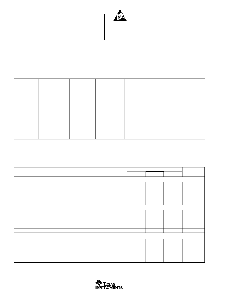
1
IN
2
OUT
3
GND
REF2912
REF2920
REF2925
REF2930
REF2933
REF2940
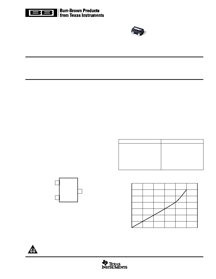
SOT23-3
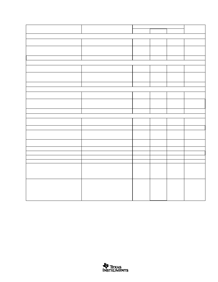
DROPOUT VOLTAGE vs LOAD CURRENT
350
300
250
200
150
100
50
0
Dropout Voltage (mV)
0
5
10
15
20
25
30
Load Current (mA)
REF2912, 2920, 2925, 2930, 2933, 2940
2
SBVS033A
www.ti.com
ELECTROSTATIC
DISCHARGE SENSITIVITY
This integrated circuit can be damaged by ESD. Texas Instru-
ments recommends that all integrated circuits be handled with
appropriate precautions. Failure to observe proper handling
and installation procedures can cause damage.
ESD damage can range from subtle performance degrada-
tion to complete device failure. Precision integrated circuits
may be more susceptible to damage because very small
parametric changes could cause the device not to meet its
published specifications.
ABSOLUTE MAXIMUM RATINGS
(1)
Supply Voltage, V+ to V≠ ................................................................... 7.0V
Output Short-Circuit
(2)
.............................................................. Continuous
Operating Temperature .................................................. ≠40
∞
C to +125
∞
C
Storage Temperature ..................................................... ≠65
∞
C to +125
∞
C
Junction Temperature .................................................................... +150
∞
C
Lead Temperature (soldering, 10s) ............................................... +300
∞
C
NOTES: (1) Stresses above these ratings may cause permanent damage.
Exposure to absolute maximum conditions for extended periods may degrade
device reliability. These are stress ratings only, and functional operation of the
device at these, or any other conditions beyond those specified, is not implied.
(2) Short-circuit to ground.
SPECIFIED
PACKAGE
TEMPERATURE
PACKAGE
ORDERING
TRANSPORT
PRODUCT
PACKAGE-LEAD
DESIGNATOR
(1)
RANGE
MARKING
NUMBER
MEDIA, QUANTITY
REF2912
SO T23-3
DBZ
≠40
∞
C to +125
∞
C
R29A
REF2912AIDBZT
Tape and Reel, 250
"
"
"
"
"
REF2912AIDBZR
Tape and Reel, 3000
REF2920
SOT23-3
DBZ
≠40
∞
C to +125
∞
C
R29B
REF2920AIDBZT
Tape and Reel, 250
"
"
"
"
"
REF2920AIDBZR
Tape and Reel, 3000
REF2925
SOT23-3
DBZ
≠40
∞
C to +125
∞
C
R29C
REF2925AIDBZT
Tape and Reel, 250
"
"
"
"
"
REF2925AIDBZR
Tape and Reel, 3000
REF2930
SOT23-3
DBZ
≠40
∞
C to +125
∞
C
R29D
REF2930AIDBZT
Tape and Reel, 250
"
"
"
"
"
REF2930AIDBZR
Tape and Reel, 3000
REF2933
SOT23-3
DBZ
≠40
∞
C to +125
∞
C
R29E
REF2933AIDBZT
Tape and Reel, 250
"
"
"
"
"
REF2933AIDBZR
Tape and Reel, 3000
REF2940
SOT23-3
DBZ
≠40
∞
C to +125
∞
C
R29F
REF2940AIDBZT
Tape and Reel, 250
"
"
"
"
"
REF2940AIDBZR
Tape and Reel, 3000
NOTE: (1) For the most current specifications and package information, refer to our web site at www.ti.com.
PACKAGE/ORDERING INFORMATION
ELECTRICAL CHARACTERISTICS
Boldface limits apply over the specified temperature range, T
A
= ≠40
∞
C to +125
∞
C.
At T
A
= +25
∞
C, I
LOAD
= 0mA, V
IN
= 5V, unless otherwise noted.
REF29xx
PARAMETER
CONDITIONS
MIN
TYP
MAX
UNITS
REF2912-1.25V
OUTPUT VOLTAGE
V
OUT
1.225
1.25
1.275
V
Initial Accuracy
2
%
NOISE
Output Voltage Noise
f = 0.1Hz to 10Hz
20
µ
Vp-p
Voltage Noise
f = 10Hz to 10kHz
42
µ
Vrms
LINE REGULATION
1.8V
V
IN
5.5V
60
190
µ
V/V
REF2920
OUTPUT VOLTAGE
V
OUT
2.007
2.048
2.089
V
Initial Accuracy
2
%
NOISE
Output Voltage Noise
f = 0.1Hz to 10Hz
28
µ
Vp-p
Voltage Noise
f = 10Hz to 10kHz
65
µ
Vrms
LINE REGULATION
V
REF
+ 50mV
V
IN
5.5V
110
290
µ
V/V
REF2925
OUTPUT VOLTAGE
V
OUT
2.450
2.50
2.550
V
Initial Accuracy
2
%
NOISE
Output Voltage Noise
f = 0.1Hz to 10Hz
35
µ
Vp-p
Voltage Noise
f = 10Hz to 10kHz
80
µ
Vrms
LINE REGULATION
V
REF
+ 50mV
V
IN
5.5V
120
325
µ
V/V
REF2912, 2920, 2925, 2930, 2933, 2940
3
SBVS033A
www.ti.com
ELECTRICAL CHARACTERISTICS
(Cont.)
Boldface limits apply over the specified temperature range, T
A
= ≠40
∞
C to +125
∞
C.
At T
A
= +25
∞
C, I
LOAD
= 0mA, V
IN
= 5V, unless otherwise noted.
REF29xx
PARAMETER
CONDITIONS
MIN
TYP
MAX
UNITS
REF2930
OUTPUT VOLTAGE
V
OUT
2.940
3.0
3.06
V
Initial Accuracy
2
%
NOISE
Output Voltage Noise
f = 0.1Hz to 10Hz
µ
Vp-p
Voltage Noise
f = 10Hz to 10kHz
µ
Vrms
LINE REGULATION
V
REF
+ 50mV
V
IN
5.5V
120
375
µ
V/V
REF2933
OUTPUT VOLTAGE
V
OUT
3.234
3.30
3.366
V
Initial Accuracy
2
%
NOISE
Output Voltage Noise
f = 0.1Hz to 10Hz
41
µ
Vp-p
Voltage Noise
f = 10Hz to 10kHz
105
µ
Vrms
LINE REGULATION
V
REF
+ 50mV
V
IN
5.5V
130
400
µ
V/V
REF2940
OUTPUT VOLTAGE
V
OUT
4.014
4.096
4.178
V
Initial Accuracy
2
%
NOISE
Output Voltage Noise
f = 0.1Hz to 10Hz
45
µ
Vp-p
Voltage Noise
f = 10Hz to 10kHz
128
µ
Vrms
LINE REGULATION
V
REF
+ 50mV
V
IN
5.5V
160
410
µ
V/V
REF2912, REF2920, REF2925, REF2930, REF2933, REF2940
OUTPUT VOLTAGE TEMP DRIFT
(2)
dV
OUT
/dT
≠40
∞
C
T
A
+125
∞
C
35
100
ppm/
∞
C
OUTPUT CURRENT
I
LOAD
25
mA
LONG-TERM STABILITY
0-1000
H
24
ppm
1000-2000
H
15
ppm
LOAD REGULATION
(3)
dV
OUT
/dI
LOAD
0mA < I
LOAD
< 25mA,
3
100
µ
V/mA
V
IN
= V
REF
+ 500mV
(1)
THERMAL HYSTERESIS
(4)
dT
25
100
ppm
DROPOUT VOLTAGE
V
IN
≠ V
OUT
1
50
mV
SHORT-CIRCUIT CURRENT
I
SC
45
mA
TURN-ON SETTLING TIME
to 0.1% at V
IN
= 5V with C
L
= 0
120
µ
s
POWER SUPPLY
Voltage
V
S
I
L
= 0
V
REF
+ 0.001
(5)
5.5
V
Over Temperature
≠40
∞
C
T
A
+125
∞
C
V
REF
+ 0.05
5.5
V
Quiescent Current
I
Q
42
50
µ
A
Over Temperature
≠40
∞
C
T
A
+125
∞
C
59
µ
A
TEMPERATURE RANGE
Specified Range
≠40
+125
∞
C
Operating Range
≠40
+125
∞
C
Storage Range
≠65
+150
∞
C
Thermal Resistance
SOT23-3 Surface-Mount
JC
110
∞
C/W
JA
336
∞
C/W
NOTES: (1) Minimum supply voltage for REF2912 is 1.8V. (2) Box Method used to determine over temperature drift. (3) Typical value of load regulation reflects
measurements using a force and sense contacts, see text "Load Regulation". (4) Thermal hysteresis procedure is explained in more detail in Applications Information
section of data sheet. (5) For I
L
> 0, see Typical Characteristic curves.
REF2912, 2920, 2925, 2930, 2933, 2940
4
SBVS033A
www.ti.com
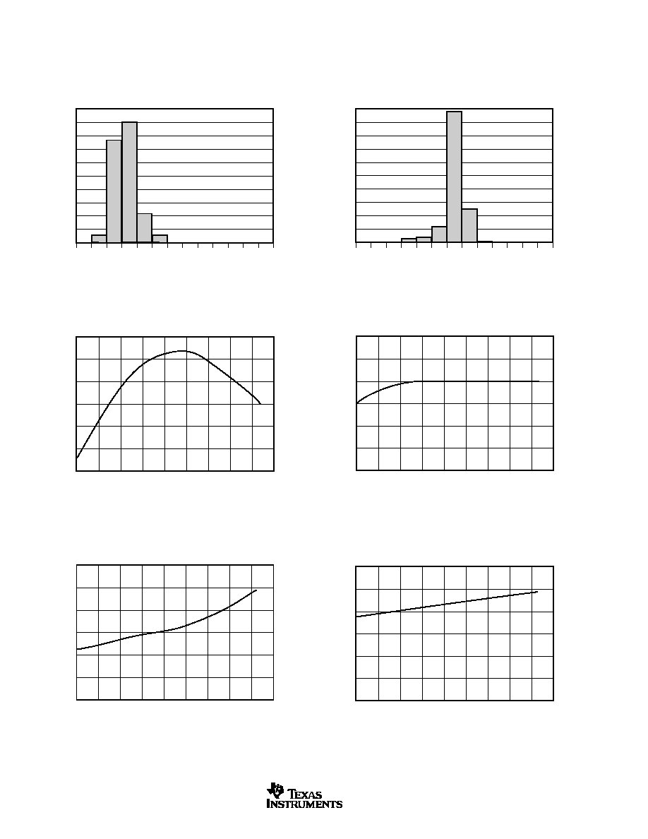
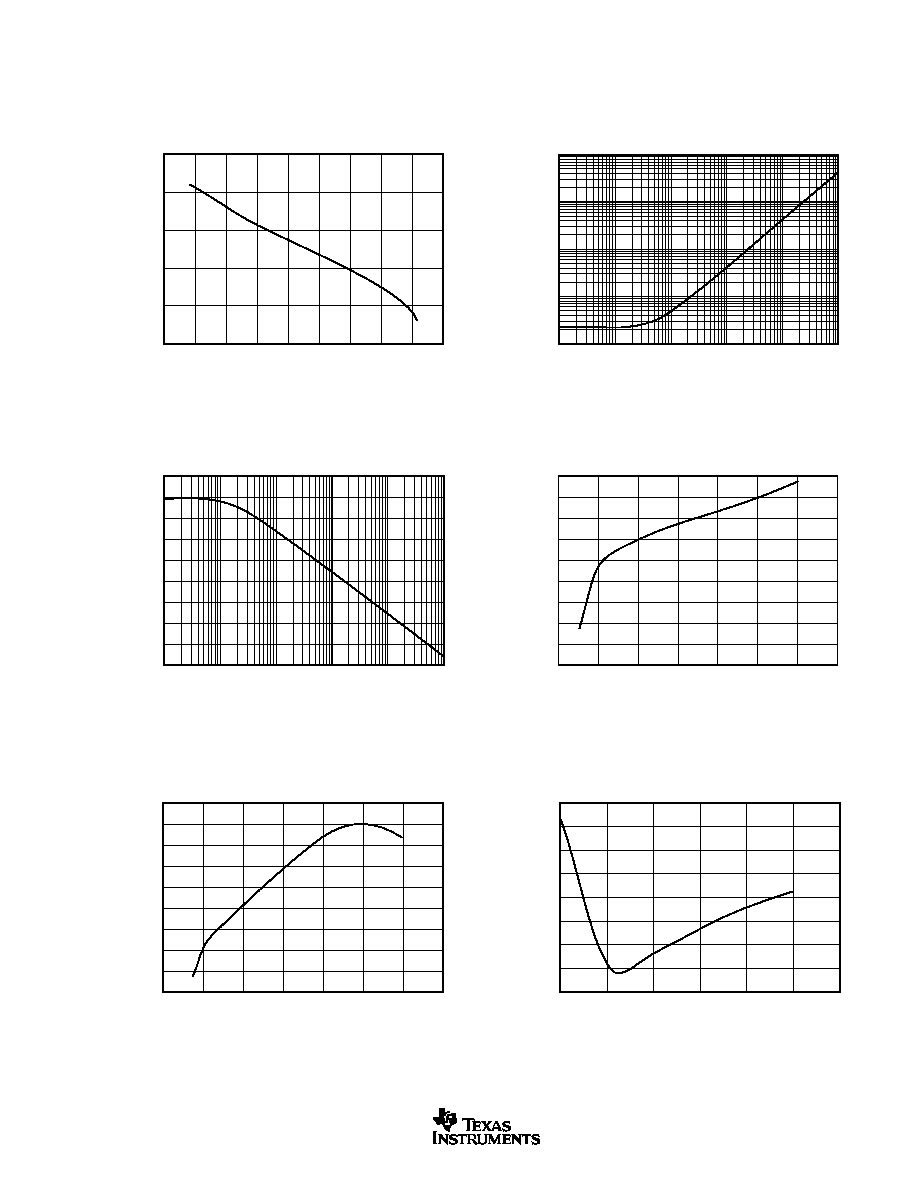
TYPICAL CHARACTERISTICS
At T
A
= +25
∞
C, V
IN
= +5V power supply, REF2925 is used for typical characteristics, unless otherwise noted.
QUIESCENT CURRENT vs TEMPERATURE
60
50
40
30
20
10
0
I
Q
(
µ
A)
Temperature (
∞
C)
≠40
≠20
0
20
60
40
80
100
120
140
TEMPERATURE DRIFT (0
∞
C to +70
∞
C)
50
45
40
35
30
25
20
15
10
5
0
Number of Units
5
10 15
20
25 30
40
35
45
50 55
65
60
Drift (ppm/
∞
C)
TEMPERATURE DRIFT (≠40
∞
C to +125
∞
C)
100
90
80
70
60
50
40
30
20
10
0
Number of Units
5
10 15
20
25 30
40
35
45
50 55
65
60
Drift (ppm/
∞
C)
LOAD REGULATION vs TEMPERATURE
6
5
4
3
2
1
0
Load Regulation (
µ
V/mA)
Temperature (
∞
C)
≠40
≠20
0
20
60
40
80
100
120
140
OUTPUT VOLTAGE vs TEMPERATURE
2.502
2.500
2.498
2.496
2.494
2.492
2.490
Output Voltage (V)
≠40
≠20
0
20
60
40
80
100
120
140
Temperature (
∞
C)
MAXIMUM LOAD CURRENT vs TEMPERATURE
35
30
25
20
15
10
5
Maximum Load Current (mA)
≠40
≠20
0
20
60
40
80
100
120
140
Temperature (
∞
C)
REF2912, 2920, 2925, 2930, 2933, 2940
5
SBVS033A
www.ti.com
TYPICAL CHARACTERISTICS
(Cont.)
At T
A
= +25
∞
C, V
IN
= +5V power supply, REF2925 is used for typical characteristics, unless otherwise noted.
OUTPUT IMPEDANCE vs FREQUENCY
100
10
1
0.1
0.01
Output Impedance (dB)
1
10
100
1k
10k
100k
Frequency (Hz)
POWER-SUPPLY REJECTION RATIO vs FREQUENCY
90
80
70
60
50
40
30
20
10
0
PSRR (dB)
1
10
100
1k
10k
100k
Frequency (Hz)
OUTPUT VOLTAGE
vs SUPPLY VOLTAGE (I
LOAD
= 25mA)
2.5008
2.5000
2.4992
2.4984
2.4976
2.4968
2.4967
2.4952
2.4944
2.4936
Output Voltage (V)
2.5
3
3.5
4
4.5
5
5.5
6
Supply (V)
OUTPUT VOLTAGE vs LOAD CURRENT
2.50152
2.50000
2.49848
2.49696
2.49544
2.49392
2.49824
2.49088
2.48936
Output Voltage (V)
0
5
10
15
20
25
30
Load Current (mA)
LINE REGULATION vs TEMPERATURE
200
150
100
50
0
≠50
Line Regulation (
µ
V/V)
Temperature (
∞
C)
≠40
≠20
0
20
60
40
80
100
120
140
OUTPUT VOLTAGE vs SUPPLY VOLTAGE (No Load)
2.50138
2.50000
2.49862
2.49724
2.49586
2.49448
2.49310
2.49172
2.49034
2.48896
Output Voltage (V)
2.5
3
3.5
4
4.5
5
5.5
6
Supply (V)