
SN65C3243, SN75C3243
3 V TO 5.5 V MULTICHANNEL COMPATIBLE RS 232 LINE DRIVERS/RECEIVERS
SLLS353D - JUNE 1999 - REVISED MARCH 2004
1
POST OFFICE BOX 655303
∑
DALLAS, TEXAS 75265
D
Operate With 3-V to 5.5-V V
CC
Supply
D
Always-Active Noninverting Receiver
Output (ROUT2B)
D
Low Standby Current . . . 1
µ
A Typical
D
External Capacitors . . . 4
◊
0.1
µ
F
D
Accept 5-V Logic Input With 3.3-V Supply
D
Inter-Operable With SN65C3238,
SN75C3238
D
Support Operation From 250 kbit/s to
1 Mbit/s
D
RS-232 Bus-Pin ESD Protection Exceeds
±
15-kV Using Human-Body Model (HBM)
D
Latch-Up Performance Exceeds 100 mA Per
JESD 78, Class II
D
Applications
- Battery-Powered Systems, PDAs,
Notebooks, Laptops, Palmtop PCs, and
Hand-Held Equipment
description/ordering information
The SN65C3243 and SN75C3243 consist of three line drivers, five line receivers, and a dual charge-pump
circuit with
±
15-kV ESD protection pin-to-pin (serial-port connection pins, including GND). These devices
provide the electrical interface between an asynchronous communication controller and the serial-port
connector. The charge pump and four small external capacitors allow operation from a single 3-V to 5.5-V
supply. In addition, these devices include an always-active noninverting output (ROUT2B), which allows
applications using the ring indicator to transmit data while the devices are powered down. The devices operate
at data signaling rates up to 1 Mbit/s and an increased slew-rate range of 24 V/
µ
s to 150 V/
µ
s.
ORDERING INFORMATION
TA
PACKAGE
ORDERABLE
PART NUMBER
TOP-SIDE
MARKING
SOIC (DW)
Tube of 20
SN75C3243DW
75C3243
SOIC (DW)
Reel of 1000
SN75C3243DWR
75C3243
-0
∞
C to 70
∞
C
SSOP (DB)
Reel of 2000
SN75C3243DBR
75C3243
-0 C to 70 C
TSSOP (PW)
Tube of 50
SN75C3243PW
CA3243
TSSOP (PW)
Reel of 2000
SN75C3243PWR
CA3243
SOIC (DW)
Tube of 20
SN65C3243DW
65C3243
SOIC (DW)
Reel of 1000
SN65C3243DWR
65C3243
-40
∞
C to 85
∞
C
SSOP (DB)
Reel of 2000
SN65C3243DBR
65C3243
-40 C to 85 C
TSSOP (PW)
Tube of 50
SN65C3243PW
65C3243
TSSOP (PW)
Reel of 2000
SN65C3243PWR
65C3243
Package drawings, standard packing quantities, thermal data, symbolization, and PCB design guidelines are
available at www.ti.com/sc/package.
Copyright
2004, Texas Instruments Incorporated
Please be aware that an important notice concerning availability, standard warranty, and use in critical applications of
Texas Instruments semiconductor products and disclaimers thereto appears at the end of this data sheet.
1
2
3
4
5
6
7
8
9
10
11
12
13
14
28
27
26
25
24
23
22
21
20
19
18
17
16
15
C2+
C2-
V-
RIN1
RIN2
RIN3
RIN4
RIN5
DOUT1
DOUT2
DOUT3
DIN3
DIN2
DIN1
C1+
V+
V
CC
GND
C1-
FORCEON
FORCEOFF
INVALID
ROUT2B
ROUT1
ROUT2
ROUT3
ROUT4
ROUT5
DB, DW, OR PW PACKAGE
(TOP VIEW)
PRODUCTION DATA information is current as of publication date.
Products conform to specifications per the terms of Texas Instruments
standard warranty. Production processing does not necessarily include
testing of all parameters.

SN65C3243, SN75C3243
3 V TO 5.5 V MULTICHANNEL COMPATIBLE RS 232 LINE DRIVERS/RECEIVERS
SLLS353D - JUNE 1999 - REVISED MARCH 2004
2
POST OFFICE BOX 655303
∑
DALLAS, TEXAS 75265
description/ordering information (continued)
Flexible control options for power management are available when the serial port is inactive. The
auto-powerdown feature functions when FORCEON is low and FORCEOFF is high. During this mode of
operation, if the devices do not sense a valid RS-232 signal, the driver outputs are disabled. If FORCEOFF is
set low, both drivers and receivers (except ROUT2B) are shut off, and the supply current is reduced to 1
µ
A.
Disconnecting the serial port or turning off the peripheral drivers causes the auto-powerdown condition to occur.
Auto-powerdown can be disabled when FORCEON and FORCEOFF are high and should be done when driving
a serial mouse. With auto-powerdown enabled, the device is activated automatically when a valid signal is
applied to any receiver input. The INVALID output is used to notify the user if an RS-232 signal is present at any
receiver input. INVALID is high (valid data) if any receiver input voltage is greater than 2.7 V or less than -2.7
V
or has been between -0.3 V and 0.3 V for less than 30
µ
s. INVALID is low (invalid data) if all receiver input
voltages are between -0.3 V and 0.3 V for more than 30
µ
s. Refer to Figure 5 for receiver input levels.
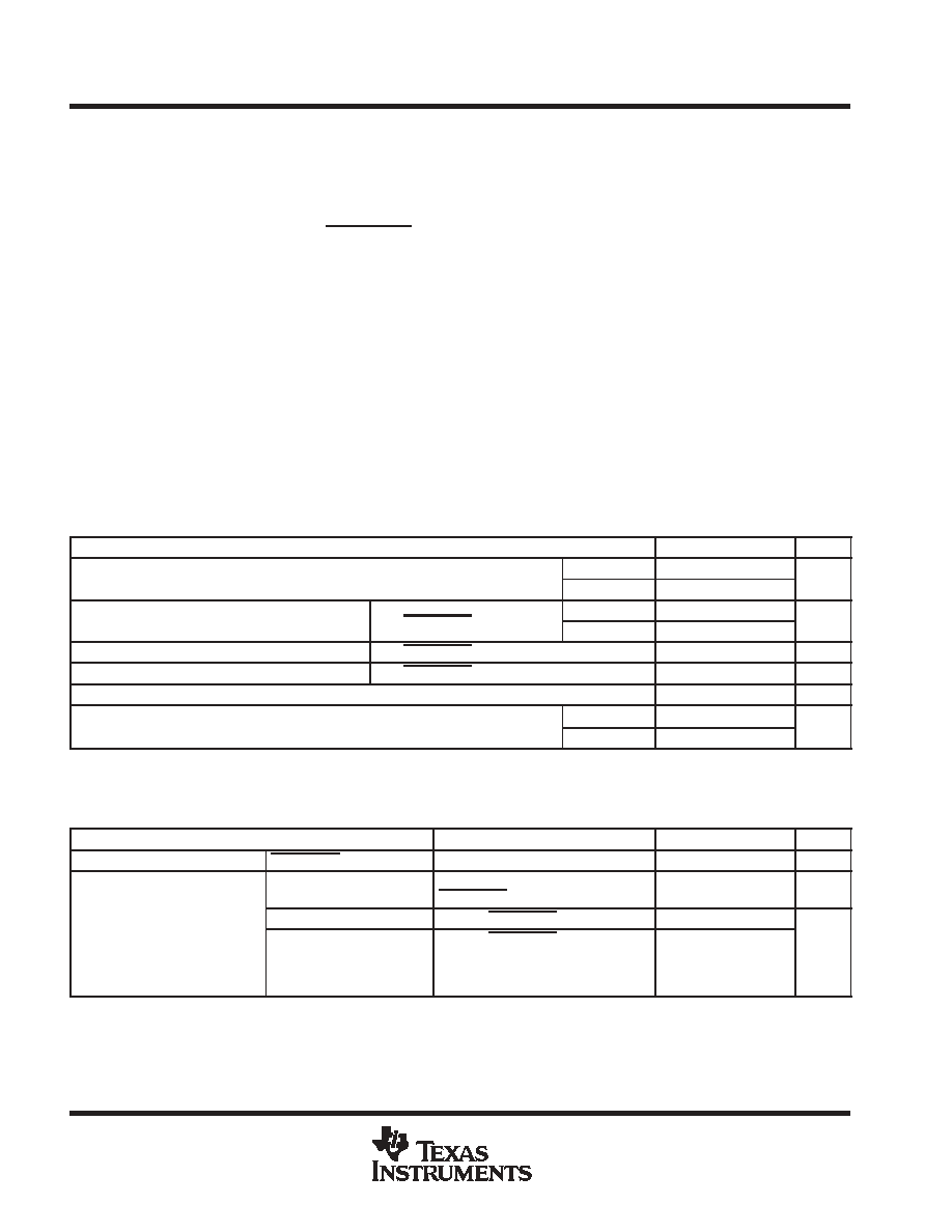
Function Tables
EACH DRIVER
INPUTS
OUTPUT
DIN
FORCEON
FORCEOFF
VALID RIN
RS-232 LEVEL
OUTPUT
DOUT
DRIVER STATUS
X
X
L
X
Z
Powered off
L
H
H
X
H
Normal operation with
H
H
H
X
L
Normal operation with
auto-powerdown disabled
L
L
H
Yes
H
Normal operation with
H
L
H
Yes
L
Normal operation with
auto-powerdown enabled
L
L
H
No
Z
Powered off by
H
L
H
No
Z
Powered off by
auto-powerdown feature
H = high level, L = low level, X = irrelevant, Z = high impedance
EACH RECEIVER
INPUTS
OUTPUTS
RIN2
RIN1,
RIN3-RIN5
FORCEOFF
VALID RIN
RS-232 LEVEL
ROUT2B
ROUT
RECEIVER STATUS
L
X
L
X
L
Z
Powered off while
H
X
L
X
H
Z
Powered off while
ROUT2B is active
L
L
H
Yes
L
H
L
H
H
Yes
L
L
Normal operation with
H
L
H
Yes
H
H
Normal operation with
auto-powerdown
disabled/enabled
H
H
H
Yes
H
L
auto-powerdown
disabled/enabled
Open
Open
H
No
L
H
H = high level, L = low level, X = irrelevant, Z = high impedance (off), Open = input disconnected or connected
driver off
SN65C3243, SN75C3243
3 V TO 5.5 V MULTICHANNEL COMPATIBLE RS 232 LINE DRIVERS/RECEIVERS
SLLS353D - JUNE 1999 - REVISED MARCH 2004
3
POST OFFICE BOX 655303
∑
DALLAS, TEXAS 75265
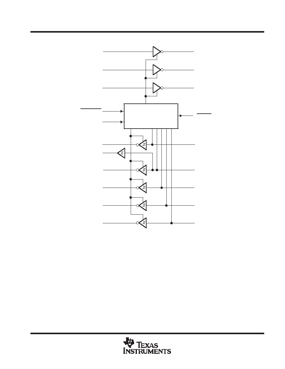
logic diagram (positive logic)
DIN3
DIN2
DIN1
DOUT3
DOUT2
DOUT1
Auto-powerdown
INVALID
RIN1
RIN2
RIN3
RIN4
RIN5
FORCEOFF
FORCEON
ROUT1
ROUT2B
ROUT2
ROUT3
ROUT4
ROUT5
14
13
12
22
23
19
20
18
17
16
15
9
10
11
21
4
5
6
7
8
SN65C3243, SN75C3243
3 V TO 5.5 V MULTICHANNEL COMPATIBLE RS 232 LINE DRIVERS/RECEIVERS
SLLS353D - JUNE 1999 - REVISED MARCH 2004
4
POST OFFICE BOX 655303
∑
DALLAS, TEXAS 75265
absolute maximum ratings over operating free-air temperature range (unless otherwise noted)
Supply voltage range, V
CC
(see Note 1)
-0.3 V to 6 V
. . . . . . . . . . . . . . . . . . . . . . . . . . . . . . . . . . . . . . . . . . . . . .
Positive output supply voltage range, V+ (see Note 1)
-0.3 V to 7 V
. . . . . . . . . . . . . . . . . . . . . . . . . . . . . . . . . .
Negative output supply voltage range, V- (see Note 1)
0.3 V to -7 V
. . . . . . . . . . . . . . . . . . . . . . . . . . . . . . . . .
Supply voltage difference, V+
-
V- (see Note 1)
13 V
. . . . . . . . . . . . . . . . . . . . . . . . . . . . . . . . . . . . . . . . . . . . . . .
Input voltage range, V
I
: Driver (FORCEOFF, FORCEON)
-0.3 V to 6 V
. . . . . . . . . . . . . . . . . . . . . . . . . . . . . . .
Receiver
-25 V to 25 V
. . . . . . . . . . . . . . . . . . . . . . . . . . . . . . . . . . . . . . . . . . . . . . . . . . . .
Output voltage range, V
O
: Driver
-13.2 V to 13.2 V
. . . . . . . . . . . . . . . . . . . . . . . . . . . . . . . . . . . . . . . . . . . . . . . . .
Package thermal impedance,
JA
(see Notes 2 and 3): DB package
62
∞
C/W
. . . . . . . . . . . . . . . . . . . . . . . . . . .
DW package
46
∞
C/W
. . . . . . . . . . . . . . . . . . . . . . . . . .
PW package
62
∞
C/W
. . . . . . . . . . . . . . . . . . . . . . . . . .
Operating virtual junction temperature, T
J
150
∞
C
. . . . . . . . . . . . . . . . . . . . . . . . . . . . . . . . . . . . . . . . . . . . . . . . . . .
Storage temperature range, T
stg
-65
∞
C to 150
∞
C
. . . . . . . . . . . . . . . . . . . . . . . . . . . . . . . . . . . . . . . . . . . . . . . . . . .
Stresses beyond those listed under "absolute maximum ratings" may cause permanent damage to the device. These are stress ratings only, and
functional operation of the device at these or any other conditions beyond those indicated under "recommended operating conditions" is not
implied. Exposure to absolute-maximum-rated conditions for extended periods may affect device reliability.
NOTES:
1. All voltages are with respect to network GND.
2. Maximum power dissipation is a function of TJ(max),
JA, and TA. The maximum allowable power dissipation at any allowable
ambient temperature is PD = (TJ(max) - TA)/
JA. Operating at the absolute maximum TJ of 150
∞
C can affect reliability.
3. The package thermal impedance is calculated in accordance with JESD 51-7.
recommended operating conditions (see Note 4 and Figure 6)
MIN
NOM
MAX
UNIT
Supply voltage
VCC = 3.3 V
3
3.3
3.6
V
Supply voltage
VCC = 5 V
4.5
5
5.5
V
VIH
Driver and control high-level input voltage
DIN, FORCEOFF, FORCEON
VCC = 3.3 V
2
V
VIH
Driver and control high-level input voltage
DIN, FORCEOFF, FORCEON
VCC = 5 V
2.4
V
VIL
Driver and control low-level input voltage
DIN, FORCEOFF, FORCEON
0.8
V
VI
Driver and control input voltage
DIN, FORCEOFF, FORCEON
0
5.5
V
VI
Receiver input voltage
-25
25
V
TA
Operating free-air temperature
SN65C3243
-40
85
∞
C
TA
Operating free-air temperature
SN75C3243
0
70
∞
C
NOTE 4: Test conditions are C1-C4 = 0.1
µ
F at VCC = 3.3 V
±
0.3 V; C1 = 0.047
µ
F, C2-C4 = 0.33
µ
F at VCC = 5 V
±
0.5 V.
electrical characteristics over recommended ranges of supply voltage and operating free-air
temperature (unless otherwise noted) (see Note 4 and Figure 6)
PARAMETER
TEST CONDITIONS
MIN
TYP
MAX
UNIT
II
Input leakage current
FORCEOFF, FORCEON
±
0.01
±
1
µ
A
Auto-powerdown disabled
No load,
FORCEOFF and FORCEON = VCC
0.3
1
mA
I
Supply current
Powered off
No load, FORCEOFF = GND
1
10
ICC
Supply current
Auto-powerdown enabled
No load, FORCEOFF = VCC,
FORCEON = GND,
All RIN are open or grounded,
All DIN are grounded
1
10
µ
A
All typical values are at VCC = 3.3 V or VCC = 5 V, and TA = 25
∞
C.
NOTE 4. Test conditions are C1-C4 = 0.1
µ
F at VCC = 3.3 V
±
0.3 V; C1 = 0.047
µ
F, C2-C4 = 0.33
µ
F at VCC = 5 V
±
0.5 V.

SN65C3243, SN75C3243
3 V TO 5.5 V MULTICHANNEL COMPATIBLE RS 232 LINE DRIVERS/RECEIVERS
SLLS353D - JUNE 1999 - REVISED MARCH 2004
5
POST OFFICE BOX 655303
∑
DALLAS, TEXAS 75265
DRIVER SECTION
electrical characteristics over recommended ranges of supply voltage and operating free-air
temperature (unless otherwise noted) (see Note 4 and Figure 6)
PARAMETER
TEST CONDITIONS
MIN
TYP
MAX
UNIT
VOH
High-level output voltage
All DOUT at RL = 3 k
to GND
5
5.4
V
VOL
Low-level output voltage
All DOUT at RL = 3 k
to GND
-5
-5.4
V
VO
Output voltage
(mouse driveability)
DIN1 = DIN2 = GND, DIN3 = VCC,
3-k
to GND at DOUT3,
DOUT1 = DOUT2 = 2.5 mA
±
5
V
IIH
High-level input current
VI = VCC
±
0.01
±
1
µ
A
IIL
Low-level input current
VI = GND
±
0.01
±
1
µ
A
IOS
Short-circuit output current
VCC = 3.6 V,
VO = 0 V
±
35
±
60
mA
IOS
Short-circuit output current
VCC = 5.5 V,
VO = 0 V
±
35
±
75
mA
ro
Output resistance
VCC, V+, and V- = 0 V, VO =
±
2 V
300
10M
Ioff
Output leakage current
FORCEOFF = GND
VO =
±
12 V,
VCC = 3 V to 3.6 V
±
25
µ
A
Ioff
Output leakage current
FORCEOFF = GND
VO =
±
10 V,
VCC = 4.5 V to 5.5 V
±
25
µ
A
All typical values are at VCC = 3.3 V or VCC = 5 V, and TA = 25
∞
C.
Short-circuit durations should be controlled to prevent exceeding the device absolute power dissipation ratings, and not more than one output
should be shorted at a time.
NOTE 4. Test conditions are C1-C4 = 0.1
µ
F at VCC = 3.3 V
±
0.3 V; C1 = 0.047
µ
F, C2-C4 = 0.33
µ
F at VCC = 5 V
±
0.5 V.
switching characteristics over recommended ranges of supply voltage and operating free-air
temperature (unless otherwise noted) (see Note 4 and Figure 6)
PARAMETER
TEST CONDITIONS
MIN
TYP
MAX
UNIT
Maximum data rate
RL = 3 k
CL = 1000 pF
250
Maximum data rate
(see Figure 1)
RL = 3 k
,
One DOUT switching
CL = 250 pF,
VCC = 3 V to 4.5 V
1000
kbit/s
(see Figure 1)
One DOUT switching
CL = 1000 pF,
VCC = 4.5 V to 5.5 V
1000
kbit/s
tsk(p)
Pulse skewß
CL = 150 pF to 2500 pF,
RL = 3 k
to 7 k
,
See Figure 2
25
ns
SR(tr)
Slew rate,
transition region
(see Figure 1)
CL = 150 pF to 1000 pF,
RL = 3 k
to 7 k
,
VCC = 3.3 V
24
150
V/
µ
s
All typical values are at VCC = 3.3 V or VCC = 5 V, and TA = 25
∞
C.
ß Pulse skew is defined as |tPLH - tPHL| of each channel of the same device.
NOTE 4. Test conditions are C1-C4 = 0.1
µ
F at VCC = 3.3 V
±
0.3 V; C1 = 0.047
µ
F, C2-C4 = 0.33
µ
F at VCC = 5 V
±
0.5 V.