Document Outline
- FEATURES
- APPLICATIONS
- DESCRIPTION
- ORDERING INFORMATION
- ABSOLUTE MAXIMUM RATINGS
- PACKAGE DISSIPATION RATINGS
- RECOMMENDED OPERATING CONDITIONS(
- SUPPLY CURRENT
- ELECTROSTATIC DISCHARGE PROTECTION
- DRIVER ELECTRICAL CHARACTERISTICS
- DRIVER SWITCHING CHARACTERISTICS
- RECEIVER ELECTRICAL CHARACTERISTICS
- RECEIVER SWITCHING CHARACTERISTICS
- PARAMETER MEASUREMENT INFORMATION
- DEVICE INFORMATION
- PIN ASSIGNMENTS
- LOGIC DIAGRAM (POSITIVE LOGIC)
- FUNCTION TABLE
- EQUIVALENT INPUT AND OUTPUT SCHEMATIC DIAGRAMS
- THERMAL CHARACTERISTICS
- TYPICAL CHARACTERISTICS
- APPLICATION INFORMATION
- POWER USAGE IN AN RS-485 TRANSCEIVER
- LOW-POWER SHUTDOWN MODE
- THERMAL CHARACTERISTICS OF IC PACKAGES

SN65HVD3082E, SN75HVD3082E
SN65HVD3085E, SN65HVD3088E
SLLS562C - MARCH 2003 - REVISED - JUNE 2004
LOW POWER RS 485 TRANSCEIVER
Available in Small MSOP-8 Package
DGK
D
P
FEATURES
D
Available in Small MSOP-8 Package
D
Meets or Exceeds the Requirements of the
TIA/EIA-485A Standard
D
Low Quiescent Power
- 0.3 mA Active Mode
- 1 nA Shutdown Mode
D
1/8 Unit Load--Up to 256 Nodes on a Bus
D
Bus-Pin ESD Protection Up to 15 kV
D
Industry-Standard SN75176 Footprint
D
Failsafe Receiver
(Bus Open, Bus Shorted, Bus Idle)
APPLICATIONS
D
Energy Meter Networks
D
Motor Control
D
Power Inverters
D
Industrial Automation
D
Building Automation Networks
D
Battery-Powered Applications
D
Telecommunications Equipment
DESCRIPTION
These devices are half-duplex transceivers designed for
RS-485 data bus networks. Powered by a 5-V supply, they
are fully compliant with TIA/EIA-485A standard. With
controlled transition times, these devices are suitable for
transmitting data over long twisted-pair cables.
SN65HVD3082E and SN75HVD3082E devices are
optimized for signaling rates up to 200 kbps.
SN65HVD3085E is suitable for data transmission up to 1
Mbps, whereas SN65HVD3088E is suitable for
applications requiring signaling rates up to 20 Mbps.
These devices are designed to operate with very low
supply current, typically 0.3 mA, exclusive of the load.
When in the inactive shutdown mode, the supply current
drops to a few nanoamps, making these devices ideal for
power-sensitive applications.
The wide common-mode range and high ESD protection
levels of these devices make them suitable for demanding
applications such as energy meter networks, electrical
inverters, status/command signals across telecom racks,
cabled chassis interconnects, and industrial automation
networks where noise tolerance is essential. These
devices match the industry-standard footprint of SN75176.
Power-on reset circuits keep the outputs in a high-
impedance state until the supply voltage has stabilized. A
thermal shutdown function protects the device from
damage due to system fault conditions. The
SN75HVD3082E is characterized for operation from 0
�
C
to 70
�
C and SN65HVD308xE are characterized for
operation from -40
�
C to 85
�
C air temperature.
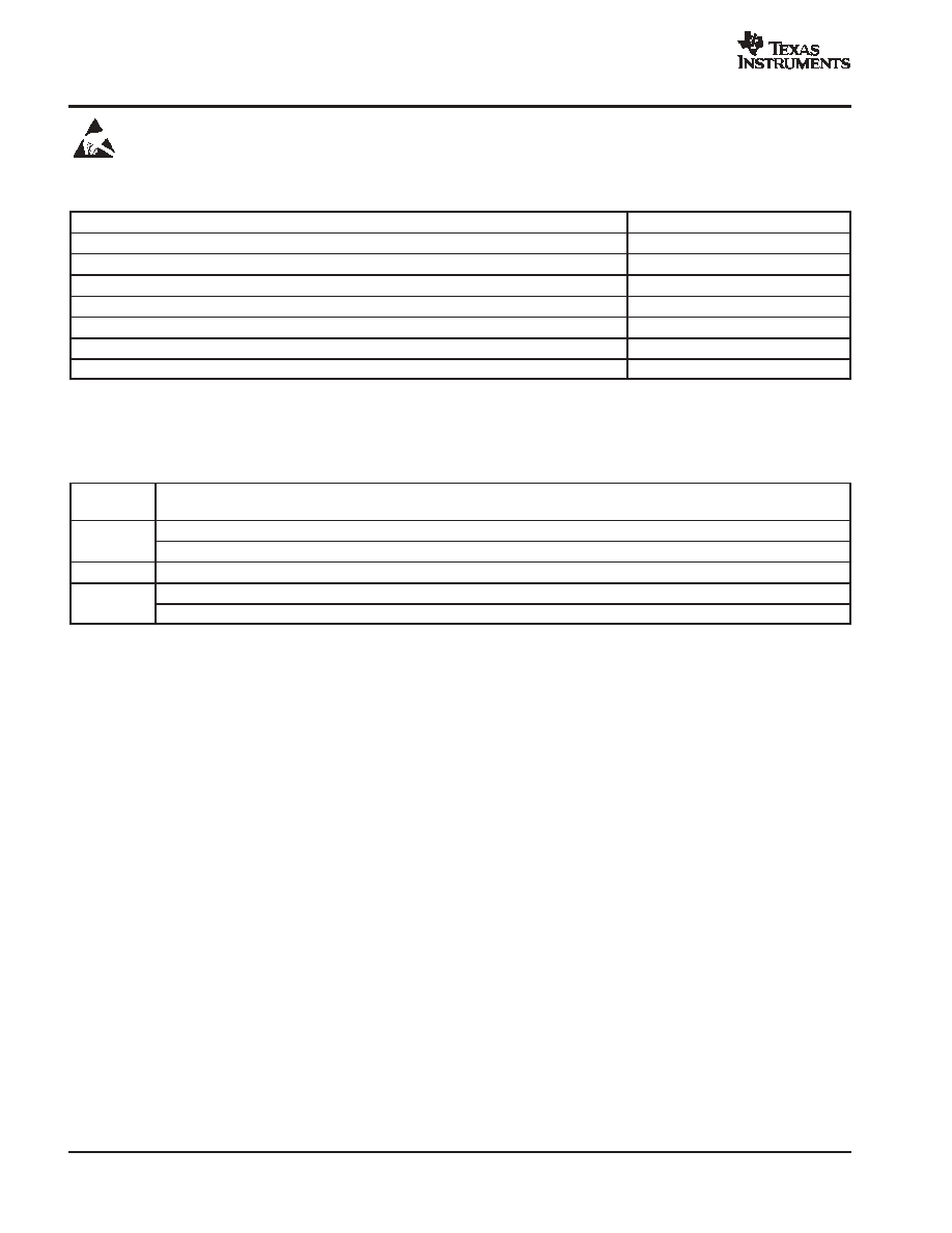
ORDERING INFORMATION
TA
SIGNALING RATE
PACKAGE TYPE
TA
SIGNALING RATE
(Mbps)
P
D(1)
DGK(2)
0
�
C to 70
�
C
0.2
SN75HVD3082EP
Marked as 75HVD3082
SN75HVD3082ED
Marked as VN3082
SN75HVD3082EDGK
Marked as NWM
0.2
SN65HVD3082EP
Marked as 65HVD3082
SN65HVD3082ED
Marked as VP3082
SN65HVD3082EDGK
Marked as NWN
-40
�
C to 85
�
C
1
SN65HVD3085ED
Marked as VP3085
SN65HVD3085EDGK
Marked as NWK
20
SN65HVD3088ED
Marked as VP3088
SN65HVD3088EDGK
Marked as NWH
(1) The D package is available taped and reeled. Add an R suffix to the device type (i.e., SN65HVD3082EDR).
(2) The DGK package is available taped and reeled. Add an R suffix to the device type (i.e., SN65HVD3082EDGKR).
PRODUCTION DATA information is current as of publication date. Products
conform to specifications per the terms of Texas Instruments standard warranty.
Production processing does not necessarily include testing of all parameters.
Please be aware that an important notice concerning availability, standard warranty, and use in critical applications of Texas Instruments
semiconductor products and disclaimers thereto appears at the end of this data sheet.
www.ti.com
Copyright
2004, Texas Instruments Incorporated
SN65HVD3082E, SN75HVD3082E
SN65HVD3085E, SN65HVD3088E
SLLS562C - MARCH 2003 - REVISED - JUNE 2004
www.ti.com
2
These devices have limited built-in ESD protection. The leads should be shorted together or the device placed in conductive foam during
storage or handling to prevent electrostatic damage to the MOS gates.
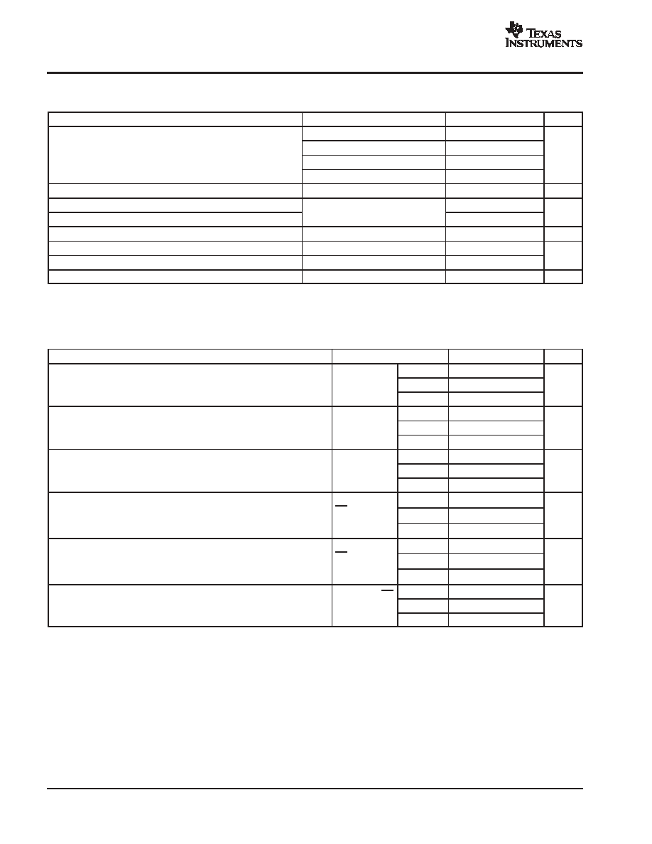
ABSOLUTE MAXIMUM RATINGS
over operating free-air temperature range unless otherwise noted(1) (2)
UNITS
Supply voltage range, VCC
-0.5 V to 7 V
Voltage range at A or B
-9 V to 14 V
Voltage range at any logic pin
-0.3 V to VCC + 0.3 V
Receiver output current
-24 mA to 24 mA
Voltage input range, transient pulse, A and B, through 100
(see Figure 13)
-50 V to 50 V
Junction temperature, TJ
170
�
C
Continuous total power dissipation
Refer to Package Dissipation Table
(1) Stresses beyond those listed under absolute maximum ratings may cause permanent damage to the device. These are stress ratings only, and
functional operation of the device at these or any other conditions beyond those indicated under recommended operating conditions is not implied.
Exposure to absolute-maximum-rated conditions for extended periods may affect device reliability.
(2) All voltage values, except differential I/O bus voltages, are with respect to network ground terminal.
PACKAGE DISSIPATION RATINGS
PACKAGE
JEDEC BOARD MODEL
TA <25
�
C
POWER RATING
DERATING FACTOR(3)
ABOVE TA = 25
�
C
TA = 70
�
C
POWER RATING
TA = 85
�
C
POWER RATING
D
Low k(1)
507 mW
4.82 mW/
�
C
289 mW
217 mW
D
High k(2)
824 mW
7.85 mW/
�
C
471 mW
353 mW
P
Low k(1)
686 mW
6.53 mW/
�
C
392 mW
294 mW
DGK
Low k(1)
394 mW
3.76 mW/
�
C
255 mW
169 mW
DGK
High k(2)
583 mW
5.55 mW/
�
C
333 mW
250 mW
(1) In accordance with the low-k thermal metric definitions of EIA/JESD51-3
(2) In accordance with the high-k thermal metric definitions of EIA/JESDS1-7
(3) This is the inverse of the junction-to-ambient thermal resistance when board-mounted and with no air flow.

SN65HVD3082E, SN75HVD3082E
SN65HVD3085E, SN65HVD3088E
SLLS562C - MARCH 2003 - REVISED - JUNE 2004
www.ti.com
3
RECOMMENDED OPERATING CONDITIONS
(1)
MIN
TYP
MAX
UNIT
Supply voltage, VCC
4.5
5.5
V
Input voltage at any bus terminal (separately or common mode), VI
-7
12
V
High-level input voltage (D, DE, or RE inputs), VIH
2
VCC
V
Low-level input voltage (D, DE, or RE inputs), VIL
0
0.8
V
Differential input voltage, VID
-12
12
V
Output current, IO
Driver
-60
60
mA
Output current, IO
Receiver
-8
8
mA
Differential load resistance, RL
54
60
SN65HVD3082E, SN75HVD3082E
0.2
Signaling rate, 1/tUI
SN65HVD3085E
1
Mbps
Signaling rate, 1/tUI
SN65HVD3088E
20
Mbps
Operating free-air temperature, TA
SN65HVD3082E, SN65HVD3085E, SN65HVD3088E
-40
85
�
C
Operating free-air temperature, TA
SN75HVD3082E
0
70
�
C
Junction temperature, TJ(2)
-40
130
�
C
(1) The algebraic convention, in which the least positive (most negative) limit is designated as minimum, is used in this data sheet.
(2) See thermal characteristics table for information on maintenance of this specification for the DGK package.
SUPPLY CURRENT
over recommended operating conditions unless otherwise noted
PARAMETER
TEST CONDITIONS
MIN
TYP(1)
MAX
UNIT
Driver and receiver enabled
D at VCC or open, DE at VCC, RE at 0 V, No load
425
900
�
A
ICC
Driver enabled, receiver disabled
D at VCC or open, DE at VCC, RE at VCC, No load
330
600
�
A
ICC
Receiver enabled, driver disabled
D at VCC or open, DE at 0 V, RE at 0 V, No load
300
600
�
A
Driver and receiver disabled
D at VCC or open, DE at 0 V, RE at VCC
0.001
2
�
A
(1) All typical values are at 25
�
C and with a 5-V supply.
ELECTROSTATIC DISCHARGE PROTECTION
PARAMETER
TEST CONDITIONS
MIN
TYP(1)
MAX
UNIT
Human body model
Bus terminals and GND
�
15
kV
Human body model(2)
All pins
�
4
kV
Charged-device-model(3)
All pins
�
1
kV
(1) All typical values at 25
�
C
(2) Tested in accordance with JEDEC Standard 22, Test Method A114-A.
(3) Tested in accordance with JEDEC Standard 22, Test Method C101.
SN65HVD3082E, SN75HVD3082E
SN65HVD3085E, SN65HVD3088E
SLLS562C - MARCH 2003 - REVISED - JUNE 2004
www.ti.com
4
DRIVER ELECTRICAL CHARACTERISTICS
over recommended operating conditions unless otherwise noted
PARAMETER
TEST CONDITIONS
MIN
TYP(1)
MAX
UNIT
IO = 0, No load
3
4.3
VOD
Differential output voltage
RL = 54
, See Figure 1
1.5
2.3
V
VOD
Differential output voltage
RL = 100
2
V
VTEST = -7 V to 12 V, See Figure 2
1.5
VOD
Change in magnitude of differential output voltage
See Figure 1 and Figure 2
-0.2
0
0.2
V
VOC(SS) Steady-state common-mode output voltage
See Figure 3
1
2.6
3
V
VOC(SS) Change in steady-state common-mode output voltage
See Figure 3
-0.1
0
0.1
V
VOC(PP)
See Figure 3
500
mV
IOZ
High-impedance output current
See receiver input currents
A
II
Input current
D, DE
-100
100
�
A
IOS
Short-circuit output current
-7 V
VO
12 V, See Figure 7
-250
250
mA
(1) All typical values are at 25
�
C and with a 5V-supply.
DRIVER SWITCHING CHARACTERISTICS
over recommended operating conditions unless otherwise noted
PARAMETER
TEST CONDITIONS
MIN
TYP
MAX
UNIT
tPLH
Propagation delay time, low-to-high-level output
RL = 54
,
HVD3082E
700
1300
tPLH
tPHL
Propagation delay time, low-to-high-level output
Propagation delay time, high-to-low-level output
RL = 54
,
CL = 50 pF,
See Figure 4
HVD3085E
150
500
ns
tPHL
Propagation delay time, high-to-low-level output
CL = 50 pF,
See Figure 4
HVD3088E
12
20
ns
tr
Differential output signal rise time
RL = 54
,
HVD3082E
500
900
1500
tr
tf
Differential output signal rise time
Differential output signal fall time
RL = 54
,
CL = 50 pF,
See Figure 4
HVD3085E
200
300
ns
tf
Differential output signal fall time
CL = 50 pF,
See Figure 4
HVD3088E
7
15
ns
RL = 54
,
HVD3082E
20
200
tsk(p)
Pulse skew ( |tPHL - tPLH| )
RL = 54
,
CL = 50 pF,
See Figure 4
HVD3085E
5
50
ns
tsk(p)
Pulse skew ( |tPHL - tPLH| )
CL = 50 pF,
See Figure 4
HVD3088E
1.4
5
ns
t
Propagation delay time, high-impedance-to-high-level output
RL = 110
,
RE at 0 V,
HVD3082E
2500
7000
tPZH
tPZL
Propagation delay time, high-impedance-to-high-level output
Propagation delay time, high-impedance-to-low-level output
RL = 110 ,
RE at 0 V,
See Figure 5
HVD3085E
1000
2500
ns
tPZL
Propagation delay time, high-impedance-to-low-level output
See Figure 5
and Figure 6
HVD3088E
13
30
ns
t
Propagation delay time, high-level-to-high-impedance output
RL = 110
,
RE at 0 V,
HVD3082E
80
200
tPHZ
tPLZ
Propagation delay time, high-level-to-high-impedance output
Propagation delay time, low-level-to-high-impedance output
RL = 110 ,
RE at 0 V,
See Figure 5
HVD3085E
60
100
ns
tPLZ
Propagation delay time, low-level-to-high-impedance output
See Figure 5
and Figure 6
HVD3088E
12
30
ns
tPZH(SHDN) Propagation delay time, shutdown-to-high-level output
RL = 110
, RE
HVD3082E
3500
7000
tPZH(SHDN)
tPZL(SHDN)
Propagation delay time, shutdown-to-high-level output
Propagation delay time, shutdown-to-low-level output
RL = 110
, RE
at VCC,
See Figure 5
HVD3085E
2500
4500
ns
tPZL(SHDN) Propagation delay time, shutdown-to-low-level output
at VCC,
See Figure 5
HVD3088E
1600
2600
ns

SN65HVD3082E, SN75HVD3082E
SN65HVD3085E, SN65HVD3088E
SLLS562C - MARCH 2003 - REVISED - JUNE 2004
www.ti.com
5
RECEIVER ELECTRICAL CHARACTERISTICS
over recommended operating conditions unless otherwise noted
PARAMETER
TEST CONDITIONS
MIN
TYP(1)
MAX
UNIT
VIT+
Positive-going input threshold voltage
IO = -8 mA
-85
-10
mV
VIT-
Negative-going input threshold voltage
IO = 8 mA
-200
-115
mV
Vhys
Hysteresis voltage (VIT+ - VIT-)
30
mV
VOH
High-level output voltage
VID = 200 mV, IOH = -8 mA, See Figure 8
4
4.6
V
VOL
Low-level output voltage
VID = -200 mV, IOH = 8 mA, See Figure 8
0.15
0.4
V
IOZ
High-impedance-state output current
VO = 0 to VCC, RE= VCC
-1
1
�
A
VIH = 12 V, VCC = 5 V
0.04
0.1
II
Bus input current
VIH = 12 V, VCC = 0
0.06
0.125
mA
II
Bus input current
VIH = -7 V, VCC = 5 V
-0.1
-0.04
mA
VIH = -7 V, VCC = 0
-0.05
-0.03
IIH
High-level input current (RE)
VIH = 2 V
-60
-30
�
A
IIL
Low-level input current (RE)
VIL = 0.8 V
-60
-30
�
A
Cdiff
Differential input capacitance
VI = 0.4 sin (4E
6
t) + 0.5 V, DE at 0 V
7
pF
(1) All typical values are at 25
�
C and with a 5-V supply.
RECEIVER SWITCHING CHARACTERISTICS
over recommended operating conditions unless otherwise noted
PARAMETER
TEST CONDITIONS
MIN
TYP
MAX
UNIT
tPLH
Propagation delay time, low-to-high-level output
HVD3082E
HVD3085E
75
200
ns
tPLH
Propagation delay time, low-to-high-level output
HVD3088E
100
ns
tPHL
Propagation delay time, high-to-low-level output
RL = 54
,
CL = 15 pF,
HVD3082E
HVD3085E
79
200
ns
tPHL
Propagation delay time, high-to-low-level output
CL = 15 pF,
See Figure 9
HVD3088E
100
ns
tsk(p)
Pulse skew ( |tPHL - tPLH| )
See Figure 9
HVD3082E
HVD3085E
4
30
ns
tsk(p)
Pulse skew ( |tPHL - tPLH| )
HVD3088E
10
ns
tr
Output signal rise time
VID = -1.5 V to 1.5 V,
1.5
3
ns
tf
Output signal fall time
VID = -1.5 V to 1.5 V,
CL = 15 pF, See Figure 9
1.8
3
ns
HVD3082E
5
50
tPZH
Output enable time to high level
HVD3082E
HVD3085E
5
50
ns
tPZH
Output enable time to high level
HVD3088E
30
ns
tPZL
Output enable time to low level
CL = 15 pF,
HVD3082E
HVD3085E
10
50
ns
tPZL
Output enable time to low level
CL = 15 pF,
DE at 3 V,
HVD3088E
30
ns
DE at 3 V,
See Figure 10
and Figure 11
HVD3082E
5
50
tPHZ
Output enable time from high level
See Figure 10
and Figure 11
HVD3082E
HVD3085E
5
50
ns
tPHZ
Output enable time from high level
HVD3088E
30
ns
tPLZ
Output enable time from low level
HVD3082E
HVD3085E
8
50
ns
tPLZ
Output enable time from low level
HVD3088E
30
ns
tPZH(SHDN) Propagation delay time, shutdown-to-high-level output
CL = 15 pF, DE at 0 V,
1600
3500
ns
tPZL(SHDN)
Propagation delay time, shutdown-to-low-level output
CL = 15 pF, DE at 0 V,
See Figure 12
1700
3500
ns