SN65LBC176A, SN75LBC176A
DIFFERENTIAL BUS TRANSCEIVERS
SLLS376C- MAY 2000 - REVISED DECEMBER 2000
1
POST OFFICE BOX 655303
∑
DALLAS, TEXAS 75265
D
High-Speed Low-Power LinBiCMOS
Circuitry Designed for Signaling Rates
Up
to 30 Mbps
D
Bus-Pin ESD Protection Exceeds 12 kV
HBM
D
Compatible With ANSI Standard
TIA/EIA-485-A and ISO 8482:1987(E)
D
Low Skew
D
Designed for Multipoint Transmission on
Long Bus Lines in Noisy Environments
D
Very Low Disabled Supply-Current
Requirements . . . 700
µ
A Maximum
D
Common Mode Voltage Range of -7 V
to 12 V
D
Thermal-Shutdown Protection
D
Driver Positive and Negative Current
Limiting
D
Open-Circuit Fail-Safe Receiver Design
D
Receiver Input Sensitivity . . .
±
200 mV Max
D
Receiver Input Hysteresis . . . 50 mV Typ
D
Glitch-Free Power-Up and Power-Down
Protection
D
Available in Q-Temp Automotive
High Reliability Automotive Applications
Configuration Control / Print Support
Qualification to Automotive Standards
description
The SN65LBC176A, SN65LBC176AQ, and
SN75LBC176A differential bus transceivers are
monolithic, integrated circuits designed for
bidirectional data communication on multipoint
bus-transmission lines. They are designed for
balanced transmission lines and are compatible
with ANSI standard TIA/EIA-485-A and ISO 8482.
The A version offers improved switching perfor-
mance over its predecessors without sacrificing
significantly more power.
Please be aware that an important notice concerning availability, standard warranty, and use in critical applications of
Texas Instruments semiconductor products and disclaimers thereto appears at the end of this data sheet.
Signaling rate by TIA/EIA-485-A definition restrict transition times to 30% of the bit length, and much higher signaling rates may be achieved
without this requirement as displayed in the TYPICAL CHARACTERISTICS of this device.
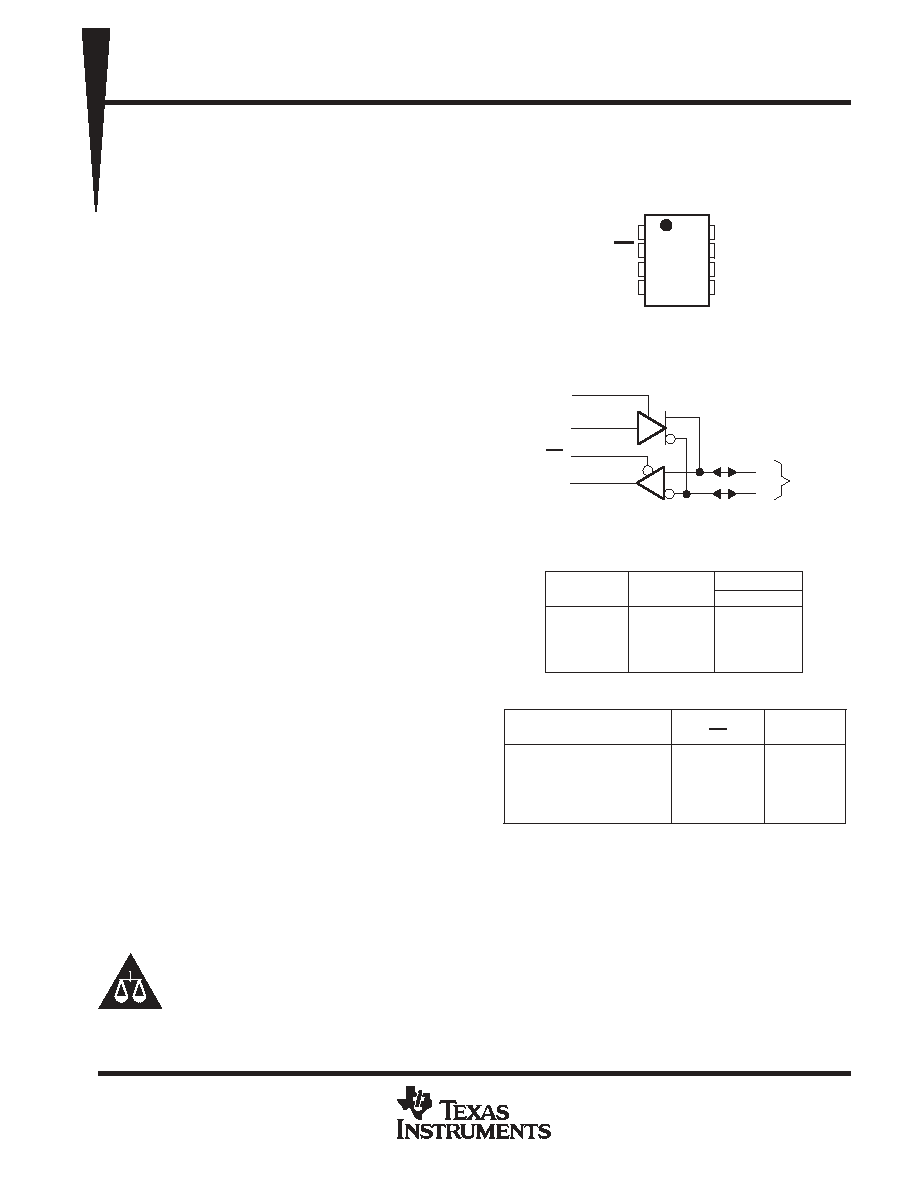
1
2
3
4
8
7
6
5
R
RE
DE
D
V
CC
B
A
GND
SN65LBC176AQD (Marked as B176AQ)
SN65LBC176AD (Marked as BL176A)
SN65LBC176AP (Marked as 65LBC176A)
SN75LBC176AD (Marked as LB176A)
SN75LBC176AP (Marked as 75LBC176A)
(TOP VIEW)
INPUT
D
H
L
X
Open
ENABLE
DE
H
H
L
H
OUTPUTS
A B
H L
L H
Z Z
H L
DRIVER
DIFFERENTIAL INPUTS
VA -VB
VID
0.2 V
- 0.2 V < VID < 0.2 V
VID
- 0.2 V
X
Open
ENABLE
RE
L
L
L
H
L
OUTPUT
R
H
?
L
Z
H
RECEIVER
H = high level, L = low level, ? = indeterminate,
X = irrelevant, Z = high impedance (off)
Function Tables
D
RE
R
7
6
4
1
2
B
A
Bus
3
DE
logic diagram (positive logic)
PRODUCTION DATA information is current as of publication date.
Products conform to specifications per the terms of Texas Instruments
standard warranty. Production processing does not necessarily include
testing of all parameters.
Copyright
2000, Texas Instruments Incorporated
LinBiCMOS and LinASIC are trademarks of Texas Instruments.
SN65LBC176A, SN75LBC176A
DIFFERENTIAL BUS TRANSCEIVERS
SLLS376C- MAY 2000 - REVISED DECEMBER 2000
2
POST OFFICE BOX 655303
∑
DALLAS, TEXAS 75265
description (continued)
The SN65LBC176A, SN65LBC176AQ, and SN75LBC176A combine a 3-state, differential line driver and a
differential input line receiver, both of which operate from a single 5-V power supply. The driver and receiver
have active-high and active-low enables, respectively, which can externally connect together to function as a
direction control. The driver differential outputs and the receiver differential inputs connect internally to form a
differential input /output (I/O) bus port that is designed to offer minimum loading to the bus whenever the driver
is disabled or V
CC
= 0. This port features wide positive and negative common-mode voltage ranges, making
the device suitable for party-line applications. Very low device supply current can be achieved by disabling the
driver and the receiver.
AVAILABLE OPTIONS
PACKAGE
TA
SMALL OUTLINE
(D)
PLASTIC
DUAL-IN-LINE
0
∞
C to 70
∞
C
SN75LBC176AD
SN75LBC176AP
- 40
∞
C to 85
∞
C
SN65LBC176AD
SN65LBC176AP
- 40
∞
C to 125
∞
C
SN65LBC176AQD
--
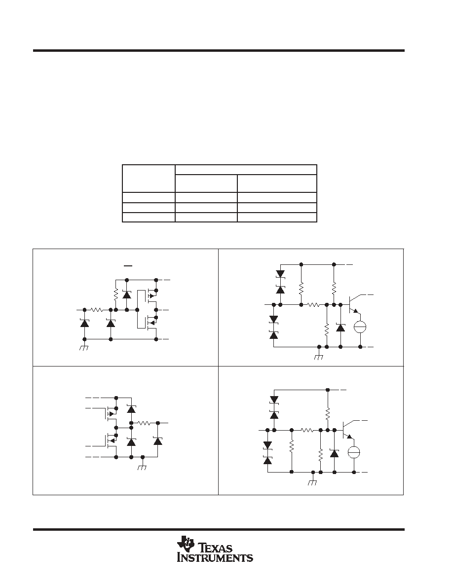
schematics of inputs and outputs
1 k
8 V
Input
VCC
Input
100 k
4 k
18 k
4 k
16 V
16 V
Input
100 k
4 k
18 k
4 k
16 V
16 V
VCC
VCC
Output
VCC
D, DE, and RE Inputs
A Input
B Input
R Output
40
8 V
100 k

SN65LBC176A, SN75LBC176A
DIFFERENTIAL BUS TRANSCEIVERS
SLLS376C- MAY 2000 - REVISED DECEMBER 2000
3
POST OFFICE BOX 655303
∑
DALLAS, TEXAS 75265
absolute maximum ratings
Supply voltage, V
CC
(see Note 1)
-0.3 V to 6 V
. . . . . . . . . . . . . . . . . . . . . . . . . . . . . . . . . . . . . . . . . . . . . . . . . . . .
Voltage range at any bus terminal (A or B)
-10 V to 15 V
. . . . . . . . . . . . . . . . . . . . . . . . . . . . . . . . . . . . . . . . . . . .
Input voltage, V
I
(D, DE, R, or RE)
-0.3 V to V
CC
+ 0.5 V
. . . . . . . . . . . . . . . . . . . . . . . . . . . . . . . . . . . . . . . . . . . .
Electrostatic discharge: Bus terminals and GND, Class 3, A: (see Note 2)
12 kV
. . . . . . . . . . . . . . . . . . . . . . . .
Bus terminals and GND, Class 3, B: (see Note 2)
400 V
. . . . . . . . . . . . . . . . . . . . . . . .
All terminals, Class 3, A:
3 kV
. . . . . . . . . . . . . . . . . . . . . . . . . . . . . . . . . . . . . . . . . . . . . . .
All terminals, Class 3, B:
400 V
. . . . . . . . . . . . . . . . . . . . . . . . . . . . . . . . . . . . . . . . . . . . .
Continuous total power dissipation (see Note 3)
See Dissipation Rating Table
. . . . . . . . . . . . . . . . . . . . . . . . . .
Storage temperature range, T
stg
-65
∞
C to 150
∞
C
. . . . . . . . . . . . . . . . . . . . . . . . . . . . . . . . . . . . . . . . . . . . . . . . . . .
Lead temperature 1,6 mm (1/16 inch) from case for 10 seconds
260
∞
C
. . . . . . . . . . . . . . . . . . . . . . . . . . . . . . .
Stresses beyond those listed under "absolute maximum ratings" may cause permanent damage to the device. These are stress ratings only, and
functional operation of the device at these or any other conditions beyond those indicated under "recommended operating conditions" is not
implied. Exposure to absolute-maximum-rated conditions for extended periods may affect device reliability.
NOTES:
1. All voltage values, except differential I/O bus voltage, are with respect to network ground terminal.
2. The maximum operating junction temperature is internally limited. Use the dissipation rating table to operate below this temperature.
3. Tested in accordance with MIL-STD-883C, Method 3015.7
DISSIPATION RATING TABLE
PACKAGE
TA
25
∞
C
POWER RATING
DERATING FACTOR
ABOVE TA = 25
∞
C
TA = 70
∞
C
POWER RATING
TA = 85
∞
C
POWER RATING
TA = 125
∞
C
POWER RATING
D
725 mW
5.8 mW/
∞
C
464 mW
377 mW
145 mW
P
1000 mW
8.0 mW/
∞
C
640 mW
520 mW
--
This is the inverse of the junction-to-ambient thermal resistance when board-mounted and with no air flow.
recommended operating conditions
MIN
NOM
MAX
UNIT
Supply voltage, VCC
4.75
5
5.25
V
Voltage at any bus terminal (separately or common mode), VI or VIC
12
V
Voltage at any bus terminal (separately or common mode), VI or VIC
-7
V
High-level input voltage, VIH (output recessive)
D, DE, and RE
2
VCC
V
Low-level input voltage, VIL (output dominant)
D, DE, and RE
0
0.8
V
Differential input voltage, VID (see Note 4)
-12ß
12
V
High-level output current, IOH
Driver
- 60
mA
High-level output current, IOH
Receiver
-8
mA
Low-level output current, IOL
Driver
60
mA
Low-level output current, IOL
Receiver
8
mA
SN65LBC176AQ
- 40
125
Operating free-air temperature, TA
SN65LBC176A
- 40
85
∞
C
Operating free-air temperature, TA
SN75LBC176A
0
70
C
ß The algebraic convention, in which the least positive (most negative) limit is designated as minimum, is used in this data sheet.
NOTE 4: Differential input /output bus voltage is measured at the noninverting terminal A with respect to the inverting terminal B.

SN65LBC176A, SN75LBC176A
DIFFERENTIAL BUS TRANSCEIVERS
SLLS376C- MAY 2000 - REVISED DECEMBER 2000
4
POST OFFICE BOX 655303
∑
DALLAS, TEXAS 75265
driver electrical characteristics over recommended operating conditions (unless otherwise noted)
PARAMETER
TEST CONDITIONS
MIN
TYP
MAX
UNIT
VIK
Input clamp voltage
II = - 18 mA
-1.5
-0.8
V
SN65LBC176AQ
1.5
4
6
IO = 0
SN65LBC176A,
SN75LBC176A
4
V
SN65LBC176AQ
0.9
1.5
6
| VOD |
Differential output voltage
RL = 54
,
See Figure 1
SN65LBC176A
1
1.5
3
V
| VOD |
Differential output voltage
RL = 54
,
See Figure 1
SN75LBC176A
1.1
1.5
3
V
SN65LBC176AQ
0.9
1.5
6
V
Vtest = - 7 V to 12 V, See Figure 2
SN65LBC176A
1
1.5
3
V
Vtest = - 7 V to 12 V, See Figure 2
SN75LBC176A
1.1
1.5
3
V
| VOD |
Change in magnitude of
differential output voltage
See Figures 1 and 2
-0.2
0.2
V
Steady-state common-mode
SN65LBC176AQ
1.8
2.4
3
VOC(SS)
Steady-state common-mode
output voltage
See Figure 1
SN65LBC176A,
SN75LBC176A
1.8
2.4
2.8
V
Change in steady-state
See Figure 1
SN65LBC176AQ
-0.2
0.2
V
VOC(SS)
Change in steady-state
common-mode output
voltage
SN65LBC176A,
SN75LBC176A
-0.1
0.1
IOZ
High-impedance output
current
See receiver input currents
IIH
High-level enable input
current
VI = 2 V
-100
µ
A
IIL
Low-level enable input current
VI = 0.8 V
-100
µ
A
IOS
Short-circuit output current
- 7 V
VO
12 V
-250
±
70
250
mA
VI = 0 or VCC,
Receiver disabled and driver enabled
5
9
ICC
Supply current
VI = 0 or VCC,
No load
Receiver disabled and driver disabled
0.4
0.7
mA
ICC
Supply current
No load
Receiver enabled and driver enabled
8.5
15
mA
All typical values are at VCC = 5 V, TA = 25
∞
C.
driver switching characteristics over recommended operating conditions (unless otherwise
noted)
PARAMETER
TEST
CONDITIONS
SN65LBC176AQ
SN65LBC176A
SN75LBC176A
UNIT
PARAMETER
CONDITIONS
MIN
TYP
MAX
MIN
TYP
MAX
UNIT
tPLH
Propagation delay time, low-to-high-level output
2
12
2
6
12
ns
tPHL
Propagation delay time, high-to-low-level output
RL = 54
,
2
12
2
6
12
ns
tsk(p)
Pulse skew ( | tPLH - tPHL | )
RL = 54
,
CL = 50 pF,
See Figure 3
2
0.3
1
ns
tr
Differential output signal rise time
CL = 50 pF,
See Figure 3
1.2
11
4
7.5
11
ns
tf
Differential output signal fall time
1.2
11
4
7.5
11
ns
tPZH
Propagation delay time, high-impedance-to-high-
level output
RL = 110
,
See Figure 4
22
12
22
ns
tPZL
Propagation delay time, high-impedance-to-low-
level output
RL = 110
,
See Figure 5
25
12
22
ns
tPHZ
Propagation delay time, high-level-to-high-
impedance output
RL = 110
,
See Figure 4
22
12
22
ns
tPLZ
Propagation delay time, low-level-to-high-
impedance output
RL = 110
,
See Figure 5
22
12
22
ns
All typical values are at VCC = 5 V, TA = 25
∞
C.

SN65LBC176A, SN75LBC176A
DIFFERENTIAL BUS TRANSCEIVERS
SLLS376C- MAY 2000 - REVISED DECEMBER 2000
5
POST OFFICE BOX 655303
∑
DALLAS, TEXAS 75265
receiver electrical characteristics over recommended operating conditions (unless otherwise
noted)
PARAMETER
TEST CONDITIONS
MIN
TYP
MAX
UNIT
VIT +
Positive-going input threshold
voltage
IO = -8 mA
0.2
V
VIT -
Negative-going input threshold
voltage
IO = 8 mA
- 0.2
V
Vhys
Hysteresis voltage (VIT + - VIT -)
IO = 8 mA
50
mV
VIK
Enable-input clamp voltage
II = - 18 mA
- 1.5
- 0.8
V
VOH
High-level output voltage
VID = 200 mV, IOH = - 8 mA,
See Figure 6
4
4.9
V
VOL
Low-level output voltage
VID = 200 mV, IOL = 8 mA,
See Figure 6
0.1
0.8
V
SN65LBC176AQ
-10
10
IOZ
High-impedance-state output current
VO = 0 to VCC
SN65LBC176A,
SN75LBC176A
-1
1
µ
A
VIH = 12 V,
VCC = 5 V
0.4
1
II
Bus input current
VIH = 12 V,
VCC = 0
Other input at 0 V
0.5
1
mA
II
Bus input current
VIH = - 7 V,
VCC = 5 V
Other input at 0 V
-0.8
- 0.4
mA
VIH = - 7 V,
VCC = 0
-0.8
- 0.3
IIH
High-level enable-input current
VIH = 2 V
- 100
µ
A
IIL
Low-level enable-input current
VIL = 0.8 V
- 100
µ
A
VI = 0 or VCC,
Receiver enabled and driver disabled
4
7
ICC
Supply current
VI = 0 or VCC,
No load
Receiver disabled and driver disabled
0.4
0.7
mA
ICC
Supply current
No load
Receiver enabled and driver enabled
8.5
15
mA
All typical values are at VCC = 5 V, TA = 25
∞
C.
receiver switching characteristics over recommended operating conditions (unless otherwise
noted)
PARAMETER
TEST CONDITIONS
SN65LBC176AQ
SN65LBC176A
SN75LBC176A
UNIT
PARAMETER
TEST CONDITIONS
MIN
TYP
MAX
MIN
TYP
MAX
UNIT
tPLH
Propagation delay time, output
VID = - 1.5 V to 1.5 V,
7
30
7
13
20
ns
tPHL
Propagation delay time, output
VID = - 1.5 V to 1.5 V,
See Figure 7
7
30
7
13
20
ns
tsk(p)
Pulse skew ( | tPHL - tPLH | )
See Figure 7
6
0.5
1.5
ns
tr
Rise time, output
See Figure 7
5
2.1
3.3
ns
tf
Fall time, output
See Figure 7
5
2.1
3.3
ns
tPZH
Output enable time to high level
50
30
45
ns
tPZL
Output enable time to low level
CL = 10 pF,
50
30
45
ns
tPHZ
Output disable time from high level
CL = 10 pF,
See Figure 8
60
20
40
ns
tPLZ
Output disable time from low level
See Figure 8
40
20
40
ns
All typical values are at VCC = 5 V, TA = 25
∞
C.