SN54ACT1284, SN74ACT1284
7 BIT BUS INTERFACES
WITH 3 STATE OUTPUTS
SCAS459D - NOVEMBER 1994 - REVISED OCTOBER 2003
1
POST OFFICE BOX 655303
∑
DALLAS, TEXAS 75265
D
4.5-V to 5.5-V V
CC
Operation
D
Inputs Accept Voltages to 5.5 V
D
Max t
pd
of 20 ns at 5 V
D
3-State Outputs Directly Drive Bus Lines
D
Flow-Through Architecture Optimizes PCB
Layout
D
Center-Pin V
CC
and GND Configurations
Minimize High-Speed Switching Noise
D
ESD Protection Exceeds JESD 22
- 2000-V Human-Body Model (A114-A)
- 200-V Machine Model (A115-A)
D
Designed for the IEEE 1284-I (Level-1 Type)
and IEEE 1284-II (Level-2 Type) Electrical
Specifications
description/ordering information
The 'ACT1284 devices are designed for
asynchronous two-way communication between
data buses. The control function minimizes
external timing requirements.
The devices allow data transmission in either the
A-to-B or the B-to-A direction for bits 1, 2, 3, and
4, depending on the logic level at the
direction-control (DIR) input. Bits 5, 6, and 7,
however, always transmit in the A-to-B direction.
The output drive for each mode is determined by the high-drive (HD) control pin. When HD is high, the high drive
is delivered by the totem-pole configuration, and when HD is low, the outputs are open drain. This meets the
drive requirements as specified in the IEEE 1284-I (level-1 type) and the IEEE 1284-II (level-2 type) parallel
peripheral-interface specification.
ORDERING INFORMATION
TA
PACKAGE
ORDERABLE
PART NUMBER
TOP-SIDE
MARKING
SOIC - DW
Tube
SN74ACT1284DW
ACT1284
SOIC - DW
Tape and reel
SN74ACT1284DWR
ACT1284
0
∞
C to 70
∞
C
SOP - NS
Tape and reel
SN74ACT1284NSR
ACT1284
0
∞
C to 70
∞
C
SSOP - DB
Tape and reel
SN74ACT1284DBR
AU284
TSSOP - PW
Tube
SN74ACT1284PW
AU284
TSSOP - PW
Tape and reel
SN74ACT1284PWR
AU284
CDIP - J
Tube
SNJ54ACT1284J
SNJ54ACT1284J
-55
∞
C to 125
∞
C
CFP - W
Tube
SNJ54ACT1284W
SNJ54ACT1284W
-55 C to 125 C
LCCC - FK
Tube
SNJ54ACT1284FK
SNJ54ACT1284FK
Package drawings, standard packing quantities, thermal data, symbolization, and PCB design guidelines are
available at www.ti.com/sc/package.
Copyright
2003, Texas Instruments Incorporated
UNLESS OTHERWISE NOTED this document contains PRODUCTION
DATA information current as of publication date. Products conform to
specifications per the terms of Texas Instruments standard warranty.
Production processing does not necessarily include testing of all
parameters.
Please be aware that an important notice concerning availability, standard warranty, and use in critical applications of
Texas Instruments semiconductor products and disclaimers thereto appears at the end of this data sheet.
1
2
3
4
5
6
7
8
9
10
20
19
18
17
16
15
14
13
12
11
A1
A2
A3
A4
GND
GND
A5
A6
A7
DIR
B1
B2
B3
B4
V
CC
V
CC
B5
B6
B7
HD
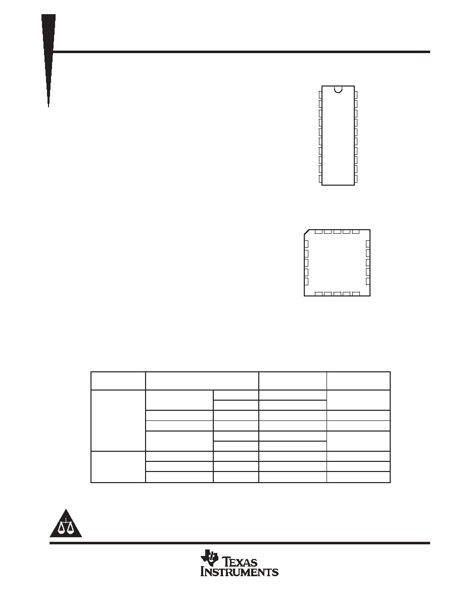
SN54ACT1284 . . . J OR W PACKAGE
SN74ACT1284 . . . DB, DW, NS, OR PW PACKAGE
(TOP VIEW)
3
2
1 20 19
9 10 11 12 13
4
5
6
7
8
18
17
16
15
14
B3
B4
V
CC
V
CC
B5
A4
GND
GND
A5
A6
SN54ACT1284 . . . FK PACKAGE
(TOP VIEW)
A3
A2
A1
B7
B6
B2
A7
DIR
HD
B1
SN54ACT1284, SN74ACT1284
7 BIT BUS INTERFACES
WITH 3 STATE OUTPUTS
SCAS459D - NOVEMBER 1994 - REVISED OCTOBER 2003
2
POST OFFICE BOX 655303
∑
DALLAS, TEXAS 75265
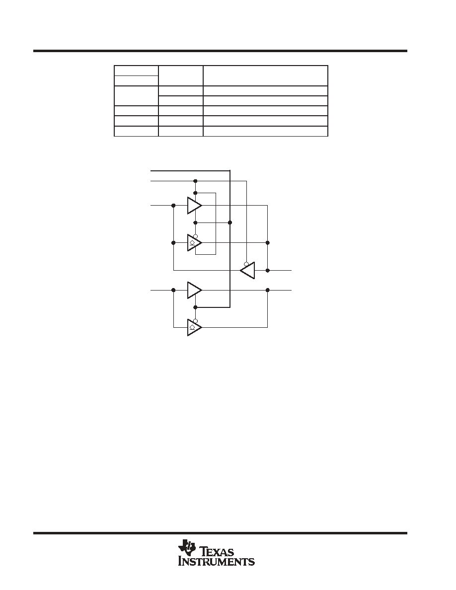
FUNCTION TABLE
INPUTS
OUTPUT
MODE
DIR
HD
OUTPUT
MODE
L
L
Open drain
A to B: Bits 5, 6, 7
L
L
Totem pole
B to A: Bits 1, 2, 3, 4
L
H
Totem pole
B to A: Bits 1, 2, 3, 4 and A to B: Bits 5, 6, 7
H
L
Open drain
A to B: Bits 1, 2, 3, 4, 5, 6, 7
H
H
Totem pole
A to B: Bits 1, 2, 3, 4, 5, 6, 7
logic diagram (positive logic)
HD
DIR
A1, A2, A3, A4
A5, A6, A7
B1, B2, B3, B4
B5, B6, B7
SN54ACT1284, SN74ACT1284
7 BIT BUS INTERFACES
WITH 3 STATE OUTPUTS
SCAS459D - NOVEMBER 1994 - REVISED OCTOBER 2003
3
POST OFFICE BOX 655303
∑
DALLAS, TEXAS 75265
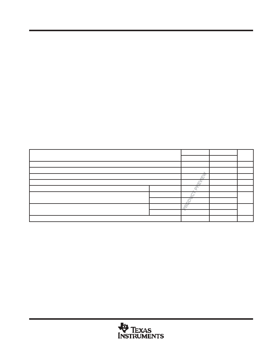
absolute maximum ratings over operating free-air temperature range (unless otherwise noted)
Supply voltage range, V
CC
-0.5 V to 7 V
. . . . . . . . . . . . . . . . . . . . . . . . . . . . . . . . . . . . . . . . . . . . . . . . . . . . . . . . . .
B-port input and output voltage range, V
I
and V
O
(see Notes 1 and 2)
-2 V to 7 V
. . . . . . . . . . . . . . . . . . . . . .
A-port input and output voltage range, V
I
and V
O
(see Note 1)
-0.5 V to V
CC
+ 0.5 V
. . . . . . . . . . . . . . . . . . . .
Input clamp current, I
IK
(V
I
< 0 or V
I
> V
CC
)
±
20 mA
. . . . . . . . . . . . . . . . . . . . . . . . . . . . . . . . . . . . . . . . . . . . . . . .
Output clamp current, I
OK
(V
O
< 0 or V
O
> V
CC
)
±
50 mA
. . . . . . . . . . . . . . . . . . . . . . . . . . . . . . . . . . . . . . . . . . . .
Continuous output current, I
O
(V
O
= 0 to V
CC
)
±
50 mA
. . . . . . . . . . . . . . . . . . . . . . . . . . . . . . . . . . . . . . . . . . . . . .
Continuous current through V
CC
or GND
±
200 mA
. . . . . . . . . . . . . . . . . . . . . . . . . . . . . . . . . . . . . . . . . . . . . . . . .
Package thermal impedance,
JA
(see Note 3): DB package
70
∞
C/W
. . . . . . . . . . . . . . . . . . . . . . . . . . . . . . . . .
DW package
58
∞
C/W
. . . . . . . . . . . . . . . . . . . . . . . . . . . . . . . . .
NS package
60
∞
C/W
. . . . . . . . . . . . . . . . . . . . . . . . . . . . . . . . .
PW package
83
∞
C/W
. . . . . . . . . . . . . . . . . . . . . . . . . . . . . . . . .
Storage temperature range, T
stg
-65
∞
C to 150
∞
C
. . . . . . . . . . . . . . . . . . . . . . . . . . . . . . . . . . . . . . . . . . . . . . . . . .
Stresses beyond those listed under "absolute maximum ratings" may cause permanent damage to the device. These are stress ratings only, and
functional operation of the device at these or any other conditions beyond those indicated under "recommended operating conditions" is not
implied. Exposure to absolute-maximum-rated conditions for extended periods may affect device reliability.
NOTES:
1. The input and output voltage ratings may be exceeded if the input and output current ratings are observed.
2. The ac input voltage pulse duration is limited to 20 ns if the input voltage goes more negative than -0.5 V.
3. The package thermal impedance is calculated in accordance with JESD 51-7.
recommended operating conditions (see Note 4)
SN54ACT1284
SN74ACT1284
UNIT
MIN
MAX
MIN
MAX
UNIT
VCC
Supply voltage
4.7
5.5
4.7
5.5
V
VIH
High-level input voltage
2
2
V
VIL
Low-level input voltage
0.8
0.8
V
VI
Input voltage
0
VCC
0
VCC
V
VO
Open-drain output voltage
HD low
0
5.5
0
5.5
V
IOH
High-level output current
B port, HD high
-14
-14
mA
IOH
High-level output current
A port
-4
-4
mA
IOL
Low-level output current
B port
14
14
mA
IOL
Low-level output current
A port
4
4
mA
TA
Operating free-air temperature
-55
125
0
70
∞
C
NOTE 4: All unused inputs of the device must be held at VCC or GND to ensure proper device operation. Refer to the TI application report,
Implications of Slow or Floating CMOS Inputs, literature number SCBA004.
PRODUCT PREVIEW information concerns products in the formative or
design phase of development. Characteristic data and other
specifications are design goals. Texas Instruments reserves the right to
change or discontinue these products without notice.
SN54ACT1284, SN74ACT1284
7 BIT BUS INTERFACES
WITH 3 STATE OUTPUTS
SCAS459D - NOVEMBER 1994 - REVISED OCTOBER 2003
4
POST OFFICE BOX 655303
∑
DALLAS, TEXAS 75265
electrical characteristics over recommended ranges of operating free-air temperature and supply
voltage (unless otherwise noted)
PARAMETER
TEST CONDITIONS
VCC
SN54ACT1284
SN74ACT1284
UNIT
PARAMETER
TEST CONDITIONS
VCC
MIN
TYP
MAX
MIN
TYP
MAX
UNIT
Vhys
Input
VIT+ - VIT- for all inputs
5 V
0.4
0.4
V
Vhys
Input
hysteresis
VIT+ - VIT- for all inputs
4.7 V
0.2
0.2
V
B port
IOH = -14 mA
4.7 V
2.4
2.4
VOH
A port
IOH = -50
µ
A
MIN
to MAX
VCC-0.2
VCC -0.2
V
A port
IOH = -4 mA
4.7 V
3.7
3.7
B port
IOL = 14 mA
4.7 V
0.4
0.4
VOL
A port
IOL = 50
µ
A
4.7 V
0.2
0.2
V
VOL
A port
IOL = 4 mA
4.7 V
0.4
0.4
V
II
VI = VCC or GND
5.5 V
±
1
±
1
µ
A
IOZ
A or B ports
VO = VCC or GND
5.5 V
±
20
±
20
µ
A
Ioff
B port
VI or VO
7 V
0 V
±
100
±
100
µ
A
ICC
VI = VCC or GND,
IO = 0
5.5 V
1.5
1.5
mA
Ci
Control inputs
VI = VCC or GND
5 V
4
4
pF
Cio
A or B ports
VO = VCC or GND
5 V
12
12
pF
ZO
B port
IOH = -20 mA,
IOH = -50 mA
5 V
8
30
8
30
For I/O ports, the parameter IOZ includes the input leakage current II.
For conditions shown as MIN or MAX, use the appropriate values under recommended operating conditions.
switching characteristics over recommended ranges of supply voltage and operating free-air
temperature (unless otherwise noted) (see Figure 1)
PARAMETER
FROM
TO
SN54ACT1284
SN74ACT1284
UNIT
PARAMETER
FROM
(INPUT)
TO
(OUTPUT)
MIN
MAX
MIN
MAX
UNIT
tPLH
Totem pole
A or B
B or A
1
20
1
20
ns
tPHL
Totem pole
A or B
B or A
1
20
1
20
ns
SR
Totem pole
B output
0.05
0.4
0.05
0.4
V/ns
tpd(EN)
Totem pole
HD
B
1
20
1
20
ns
tpd(DIS)
Totem pole
HD
B
1
20
1
20
ns
tr, tf
Open drain
A
B
120
120
ns
PRODUCT PREVIEW information concerns products in the formative or
design phase of development. Characteristic data and other
specifications are design goals. Texas Instruments reserves the right to
change or discontinue these products without notice.
SN54ACT1284, SN74ACT1284
7 BIT BUS INTERFACES
WITH 3 STATE OUTPUTS
SCAS459D - NOVEMBER 1994 - REVISED OCTOBER 2003
5
POST OFFICE BOX 655303
∑
DALLAS, TEXAS 75265
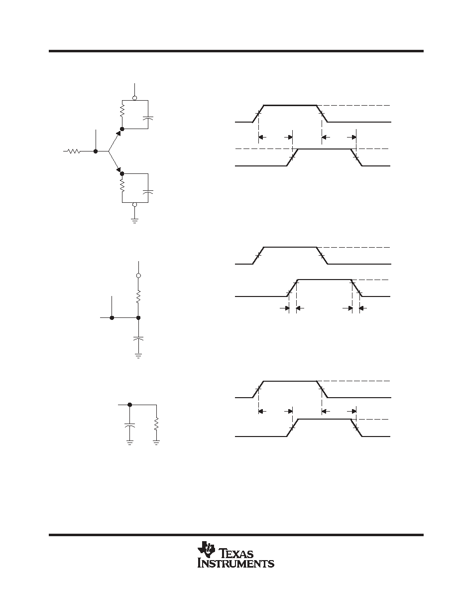
PARAMETER MEASUREMENT INFORMATION
50% VCC
tPHL
tPLH
From B Output
Under Test
A-TO-B LOAD (totem pole)
1.5 V
VOLTAGE WAVEFORMS MEASURED AT TP1
PROPAGATION DELAY TIMES (A to B)
3 V
VOH
VOL
VOL
0 V
62
CL = 50 pF
(see Note A)
33
TP1
VCC
CL = 50 pF
(see Note A)
Sink Load
Source Load
1.5 V
1.5 V
VOH
VOL
VOH - 1.4 V
VOH - 1.4 V
VOL + 1.4 V
62
tPHL
tPLH
tf
A-TO-B LOAD (open drain)
1.5 V
VOLTAGE WAVEFORMS MEASURED AT TP1 (B SIDE)
3 V
VOH
VOL
0 V
TP1
VCC
CL = 50 pF
(see Note A)
1.5 V
VOL
(see Note E)
0.8 V
500
From B Output
tr
2 V
2 V
0.8 V
tPHL
tPLH
1.5 V
VOLTAGE WAVEFORMS
PROPAGATION DELAY TIMES (B to A)
3 V
VOH
VOL
VOL
0 V
1.5 V
1.5 V
Output
50% VCC
B-TO-A LOAD (totem pole)
CL = 50 pF
(see Note A)
500
From A Output
Under Test
Input
(see Note C)
Output
(see Note D)
Input
(see Note F)
Input
(see Note F)
NOTES: A. CL includes probe and jig capacitance.
B. The outputs are measured one at a time with one transition per measurement.
C. Input rise and fall times are 3 ns, 150 ns < pulse duration <10
µ
s for both low-to-high and high-to-low transitions.
D. Slew rate is defined as 10% and 90% of the transition times.
E. Rise and fall times, open drain, are <120 ns.
F. Input rise and fall times are 3 ns.
Figure 1. Load Circuits and Voltage Waveforms