Äîêóìåíòàöèÿ è îïèñàíèÿ www.docs.chipfind.ru
SN54AHC139, SN74AHC139
DUAL 2-LINE TO 4-LINE DECODERS/DEMULTIPLEXERS
SCLS259K DECEMBER 1995 REVISED MARCH 2003
1
POST OFFICE BOX 655303
·
DALLAS, TEXAS 75265
D
Operating Range 2-V to 5.5-V V
CC
D
Designed Specifically for High-Speed
Memory Decoders and Data-Transmission
Systems
D
Incorporate Two Enable Inputs to Simplify
Cascading and/or Data Reception
D
Latch-Up Performance Exceeds 250 mA Per
JESD 17
D
ESD Protection Exceeds JESD 22
2000-V Human-Body Model (A114-A)
200-V Machine Model (A115-A)
1000-V Charged-Device Model (C101)
3
2 1 20 19
9 10 11 12 13
4
5
6
7
8
18
17
16
15
14
2A
2B
NC
2Y0
2Y1
1B
1Y0
NC
1Y1
1Y2
1A
1G
NC
2Y3
2Y2
V
2G
1Y3
GND
NC
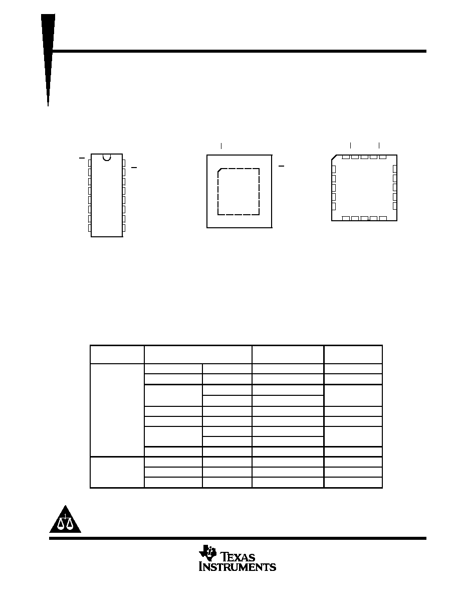
SN54AHC139 . . . FK PACKAGE
(TOP VIEW)
CC
NC No internal connection
1
2
3
4
5
6
7
8
16
15
14
13
12
11
10
9
1G
1A
1B
1Y0
1Y1
1Y2
1Y3
GND
V
CC
2G
2A
2B
2Y0
2Y1
2Y2
2Y3
SN54AHC139 . . . J OR W PACKAGE
SN74AHC139 . . . D, DB, DGV, N, NS
OR PW PACKAGE
(TOP VIEW)
SN74AHC139 . . . RGY PACKAGE
(TOP VIEW)
1
16
8
9
2
3
4
5
6
7
15
14
13
12
11
10
2G
2A
2B
2Y0
2Y1
2Y2
1A
1B
1Y0
1Y1
1Y2
1Y3
1G
2Y3
V
GND
CC
description/ordering information
The 'AHC139 devices are dual 2-line to 4-line decoders/demultiplexers designed for 2-V to 5.5-V V
CC
operation.
These devices are designed to be used in high-performance memory-decoding or data-routing applications
requiring very short propagation delay times. In high-performance memory systems, these decoders can be
used to minimize the effects of system decoding. When used with high-speed memories utilizing a fast enable
circuit, the delay times of these decoders and the enable time of the memory usually are less than the typical
access time of the memory. This means that the effective system delay introduced by the decoders is negligible.
ORDERING INFORMATION
TA
PACKAGE
ORDERABLE
PART NUMBER
TOP-SIDE
MARKING
QFN RGY
Tape and reel
SN74AHC139RGYR
HA139
PDIP N
Tube
SN74AHC139N
SN74AHC139N
SOIC D
Tube
SN74AHC139D
AHC139
SOIC D
Tape and reel
SN74AHC139DR
AHC139
40
°
C to 85
°
C
SOP NS
Tape and reel
SN74AHC139NSR
AHC139
SSOP DB
Tape and reel
SN74AHC139DBR
HA139
TSSOP
PW
Tube
SN74AHC139PW
HA139
TSSOP PW
Tape and reel
SN74AHC139PWR
HA139
TVSOP DGV
Tape and reel
SN74AHC139DGVR
HA139
CDIP J
Tube
SNJ54AHC139J
SNJ54AHC139J
55
°
C to 125
°
C
CFP W
Tube
SNJ54AHC139W
SNJ54AHC139W
LCCC FK
Tube
SNJ54AHC139FK
SNJ54AHC139FK
Package drawings, standard packing quantities, thermal data, symbolization, and PCB design guidelines
are available at www.ti.com/sc/package.
Copyright
2003, Texas Instruments Incorporated
UNLESS OTHERWISE NOTED this document contains PRODUCTION
DATA information current as of publication date. Products conform to
specifications per the terms of Texas Instruments standard warranty.
Production processing does not necessarily include testing of all
parameters.
Please be aware that an important notice concerning availability, standard warranty, and use in critical applications of
Texas Instruments semiconductor products and disclaimers thereto appears at the end of this data sheet.
SN54AHC139, SN74AHC139
DUAL 2-LINE TO 4-LINE DECODERS/DEMULTIPLEXERS
SCLS259K DECEMBER 1995 REVISED MARCH 2003
2
POST OFFICE BOX 655303
·
DALLAS, TEXAS 75265
description/ordering information (continued)
The active-low enable (G) input can be used as a data line in demultiplexing applications. These
decoders/demultiplexers feature fully buffered inputs, each of which represents only one normalized load to its
driving circuit.
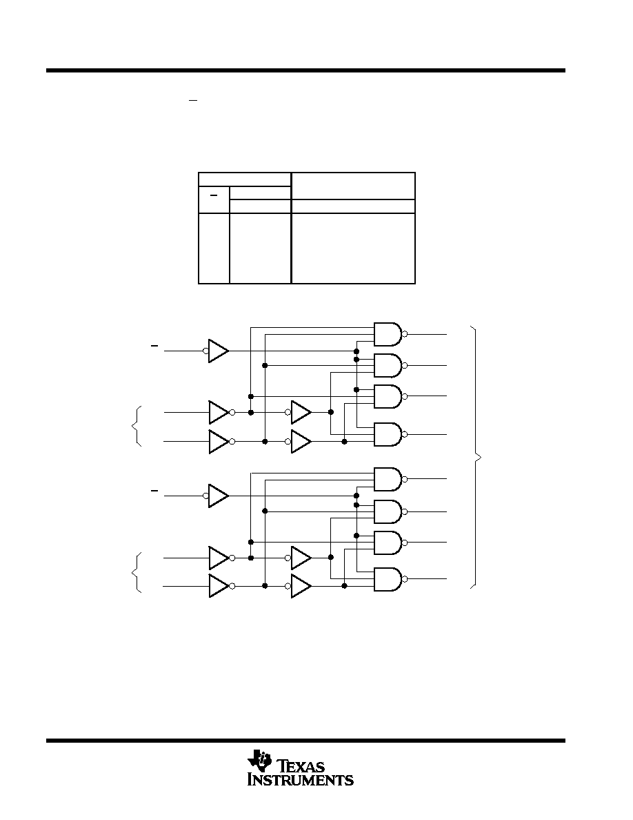
FUNCTION TABLE
(each decoder/demultiplexer)
INPUTS
OUTPUTS
G
SELECT
OUTPUTS
G
B
A
Y0
Y1
Y2
Y3
H
X
X
H
H
H
H
L
L
L
L
H
H
H
L
L
H
H
L
H
H
L
H
L
H
H
L
H
L
H
H
H
H
H
L
logic diagram (positive logic)
Select
Inputs
Select
Inputs
2B
2A
2G
1B
1A
1G
Data
Outputs
2Y3
2Y2
2Y1
2Y0
1Y3
1Y2
1Y1
1Y0
1
2
3
15
14
13
4
5
6
7
12
11
10
9
Pin numbers shown are for the D, DB, DGV, J, N, NS, PW, RGY, and W packages.
SN54AHC139, SN74AHC139
DUAL 2-LINE TO 4-LINE DECODERS/DEMULTIPLEXERS
SCLS259K DECEMBER 1995 REVISED MARCH 2003
3
POST OFFICE BOX 655303
·
DALLAS, TEXAS 75265
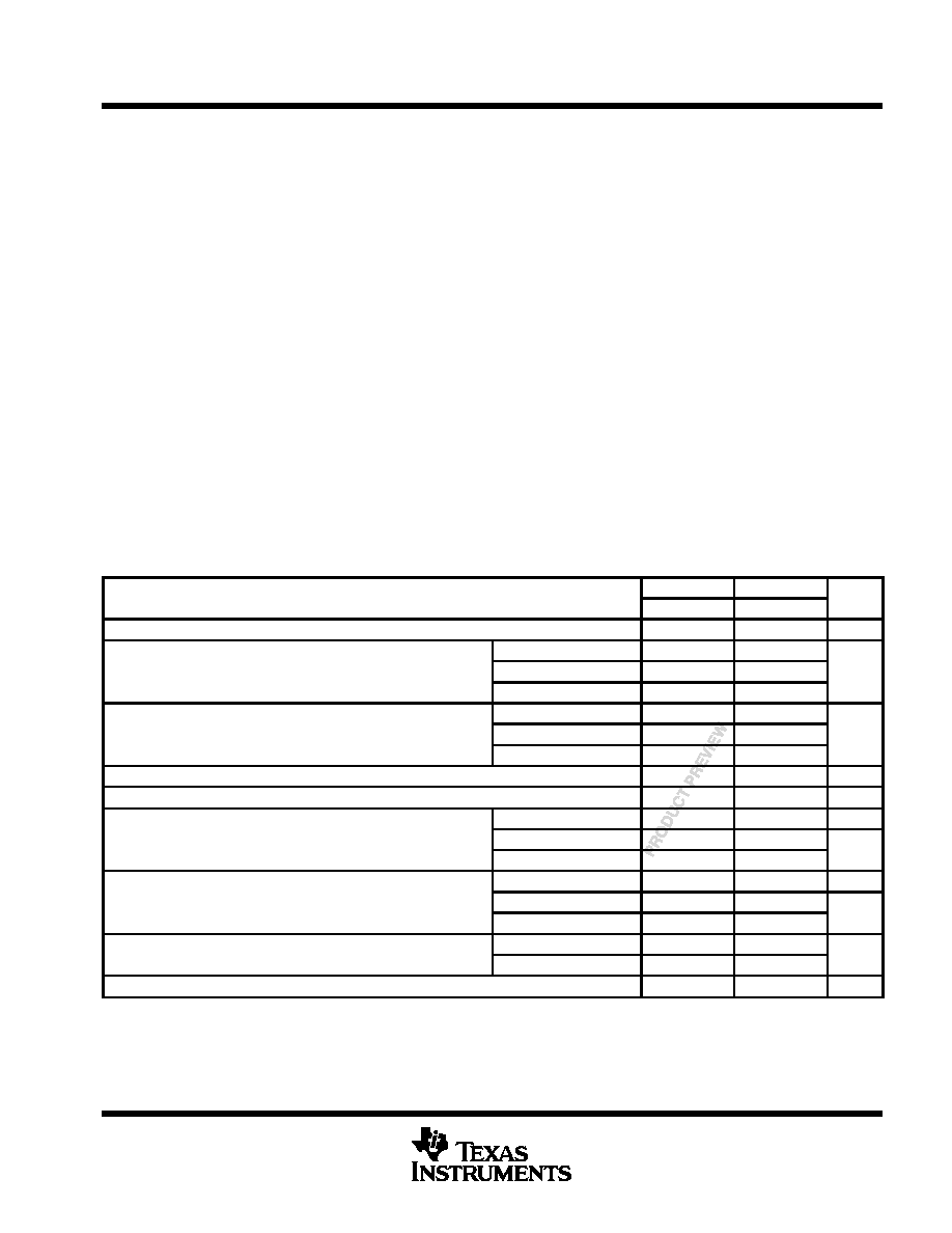
absolute maximum ratings over operating free-air temperature range (unless otherwise noted)
Supply voltage range, V
CC
0.5 V to 7 V
. . . . . . . . . . . . . . . . . . . . . . . . . . . . . . . . . . . . . . . . . . . . . . . . . . . . . . . . . .
Input voltage range, V
I
(see Note 1)
0.5 V to 7 V
. . . . . . . . . . . . . . . . . . . . . . . . . . . . . . . . . . . . . . . . . . . . . . . . . .
Output voltage range, V
O
(see Note 1)
0.5 V to V
CC
+ 0.5 V
. . . . . . . . . . . . . . . . . . . . . . . . . . . . . . . . . . . . . . . .
Input clamp current, I
IK
(V
I
< 0)
20 mA
. . . . . . . . . . . . . . . . . . . . . . . . . . . . . . . . . . . . . . . . . . . . . . . . . . . . . . . . . . .
Output clamp current, I
OK
(V
O
< 0 or V
O
> V
CC
)
±
20 mA
. . . . . . . . . . . . . . . . . . . . . . . . . . . . . . . . . . . . . . . . . . . .
Continuous output current, I
O
(V
O
= 0 to V
CC
)
±
25 mA
. . . . . . . . . . . . . . . . . . . . . . . . . . . . . . . . . . . . . . . . . . . . . .
Continuous current through V
CC
or GND
±
75 mA
. . . . . . . . . . . . . . . . . . . . . . . . . . . . . . . . . . . . . . . . . . . . . . . . . . .
Package thermal impedance,
JA
(see Note 2): D package
73
°
C/W
. . . . . . . . . . . . . . . . . . . . . . . . . . . . . . . . . . .
(see Note 2): DB package
82
°
C/W
. . . . . . . . . . . . . . . . . . . . . . . . . . . . . . . . .
(see Note 2): DGV package
120
°
C/W
. . . . . . . . . . . . . . . . . . . . . . . . . . . . . . .
(see Note 2): N package
67
°
C/W
. . . . . . . . . . . . . . . . . . . . . . . . . . . . . . . . . . .
(see Note 2): NS package
64
°
C/W
. . . . . . . . . . . . . . . . . . . . . . . . . . . . . . . . .
(see Note 2): PW package
108
°
C/W
. . . . . . . . . . . . . . . . . . . . . . . . . . . . . . . .
(see Note 3): RGY package
39
°
C/W
. . . . . . . . . . . . . . . . . . . . . . . . . . . . . . . .
Storage temperature range, T
stg
65
°
C to 150
°
C
. . . . . . . . . . . . . . . . . . . . . . . . . . . . . . . . . . . . . . . . . . . . . . . . . . .
Stresses beyond those listed under "absolute maximum ratings" may cause permanent damage to the device. These are stress ratings only, and
functional operation of the device at these or any other conditions beyond those indicated under "recommended operating conditions" is not
implied. Exposure to absolute-maximum-rated conditions for extended periods may affect device reliability.
NOTES:
1. The input and output voltage ratings may be exceeded if the input and output current ratings are observed.
2. The package thermal impedance is calculated in accordance with JESD 51-7.
3. The package thermal impedance is calculated in accordance with JESD 51-5.
recommended operating conditions (see Note 4)
SN54AHC139
SN74AHC139
UNIT
MIN
MAX
MIN
MAX
UNIT
VCC
Supply voltage
2
5.5
2
5.5
V
VCC = 2 V
1.5
1.5
VIH
High-level input voltage
VCC = 3 V
2.1
2.1
V
VCC = 5.5 V
3.85
3.85
VCC = 2 V
0.5
0.5
VIL
Low-level input voltage
VCC = 3 V
0.9
0.9
V
VCC = 5.5 V
1.65
1.65
VI
Input voltage
0
5.5
0
5.5
V
VO
Output voltage
0
VCC
0
VCC
V
VCC = 2 V
50
50
m
A
IOH
High-level output current
VCC = 3.3 V
±
0.3 V
4
4
mA
VCC = 5 V
±
0.5 V
8
8
mA
VCC = 2 V
50
50
m
A
IOL
Low-level output current
VCC = 3.3 V
±
0.3 V
4
4
mA
VCC = 5 V
±
0.5 V
8
8
mA
t/
v
Input transition rise or fall rate
VCC = 3.3 V
±
0.3 V
100
100
ns/V
t/
v
Input transition rise or fall rate
VCC = 5 V
±
0.5 V
20
20
ns/V
TA
Operating free-air temperature
55
125
40
85
°
C
NOTE 4: All unused inputs of the device must be held at VCC or GND to ensure proper device operation. Refer to the TI application report,
Implications of Slow or Floating CMOS Inputs, literature number SCBA004.
PRODUCT PREVIEW information concerns products in the formative or
design phase of development. Characteristic data and other
specifications are design goals. Texas Instruments reserves the right to
change or discontinue these products without notice.
SN54AHC139, SN74AHC139
DUAL 2-LINE TO 4-LINE DECODERS/DEMULTIPLEXERS
SCLS259K DECEMBER 1995 REVISED MARCH 2003
4
POST OFFICE BOX 655303
·
DALLAS, TEXAS 75265
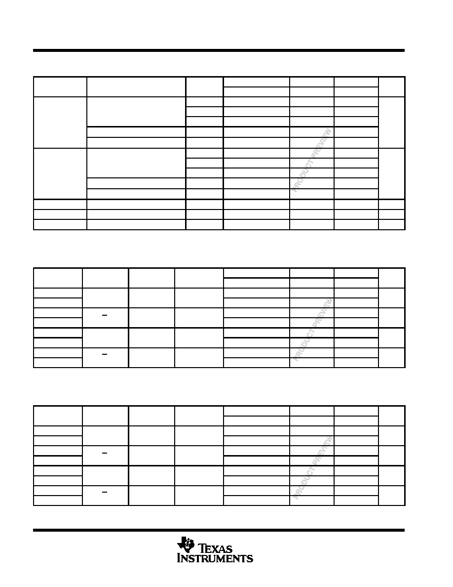
electrical characteristics over recommended operating free-air temperature range (unless
otherwise noted)
PARAMETER
TEST CONDITIONS
VCC
TA = 25
°
C
SN54AHC139
SN74AHC139
UNIT
PARAMETER
TEST CONDITIONS
VCC
MIN
TYP
MAX
MIN
MAX
MIN
MAX
UNIT
2 V
1.9
2
1.9
1.9
IOH = 50
m
A
3 V
2.9
3
2.9
2.9
VOH
4.5 V
4.4
4.5
4.4
4.4
V
OH
IOH = 4 mA
3 V
2.58
2.48
2.48
IOH = 8 mA
4.5 V
3.94
3.8
3.8
2 V
0.1
0.1
0.1
IOL = 50
m
A
3 V
0.1
0.1
0.1
VOL
4.5 V
0.1
0.1
0.1
V
OL
IOL = 4 mA
3 V
0.36
0.5
0.44
IOL = 8 mA
4.5 V
0.36
0.5
0.44
II
VI = 5.5 V or GND
0 V to 5.5 V
±
0.1
±
1*
±
1
m
A
ICC
VI = VCC or GND,
IO = 0
5.5 V
4
40
40
m
A
Ci
VI = VCC or GND
5 V
2
10
10
pF
* On products compliant to MIL-PRF-38535, this parameter is not production tested at VCC = 0 V.
switching characteristics over recommended operating free-air temperature range,
V
CC
= 3.3 V
±
0.3 V (unless otherwise noted) (see Figure 1)
PARAMETER
FROM
TO
LOAD
TA = 25
°
C
SN54AHC139
SN74AHC139
UNIT
PARAMETER
(INPUT)
(OUTPUT)
CAPACITANCE
MIN
TYP
MAX
MIN
MAX
MIN
MAX
UNIT
tPLH
A or B
Y
CL = 15 pF
7.2**
11**
1**
13**
1
13
ns
tPHL
A or B
Y
CL = 15 pF
7.2**
11**
1**
13**
1
13
ns
tPLH
G
Y
CL = 15 pF
6.4**
9.2**
1**
11**
1
11
ns
tPHL
G
Y
CL = 15 pF
6.4**
9.2**
1**
11**
1
11
ns
tPLH
A or B
Y
CL = 50 pF
9.7
14.5
1
16.5
1
16.5
ns
tPHL
A or B
Y
CL = 50 pF
9.7
14.5
1
16.5
1
16.5
ns
tPLH
G
Y
CL = 50 pF
8.9
12.7
1
14.5
1
14.5
ns
tPHL
G
Y
CL = 50 pF
8.9
12.7
1
14.5
1
14.5
ns
** On products compliant to MIL-PRF-38535, this parameter is not production tested.
switching characteristics over recommended operating free-air temperature range,
V
CC
= 5 V
±
0.5 V (unless otherwise noted) (see Figure 1)
PARAMETER
FROM
TO
LOAD
TA = 25
°
C
SN54AHC139
SN74AHC139
UNIT
PARAMETER
(INPUT)
(OUTPUT)
CAPACITANCE
MIN
TYP
MAX
MIN
MAX
MIN
MAX
UNIT
tPLH
A or B
Y
CL = 15 pF
5**
7.2**
1**
8.5**
1
8.5
ns
tPHL
A or B
Y
CL = 15 pF
5**
7.2**
1**
8.5**
1
8.5
ns
tPLH
G
Y
CL = 15 pF
4.4**
6.3**
1**
7.5**
1
7.5
ns
tPHL
G
Y
CL = 15 pF
4.4**
6.3**
1**
7.5**
1
7.5
ns
tPLH
A or B
Y
CL = 50 pF
6.5
9.2
1
10.5
1
10.5
ns
tPHL
A or B
Y
CL = 50 pF
6.5
9.2
1
10.5
1
10.5
ns
tPLH
G
Y
CL = 50 pF
5.9
8.3
1
9.5
1
9.5
ns
tPHL
G
Y
CL = 50 pF
5.9
8.3
1
9.5
1
9.5
ns
** On products compliant to MIL-PRF-38535, this parameter is not production tested.
PRODUCT PREVIEW information concerns products in the formative or
design phase of development. Characteristic data and other
specifications are design goals. Texas Instruments reserves the right to
change or discontinue these products without notice.
SN54AHC139, SN74AHC139
DUAL 2-LINE TO 4-LINE DECODERS/DEMULTIPLEXERS
SCLS259K DECEMBER 1995 REVISED MARCH 2003
5
POST OFFICE BOX 655303
·
DALLAS, TEXAS 75265
operating characteristics, V
CC
= 5 V, T
A
= 25
°
C
PARAMETER
TEST CONDITIONS
TYP
UNIT
Cpd
Power dissipation capacitance
No load,
f = 1 MHz
13
pF
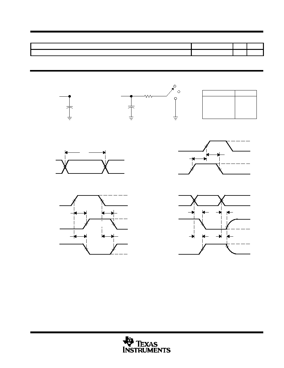
PARAMETER MEASUREMENT INFORMATION
50% VCC
VCC
VCC
0 V
0 V
th
tsu
VOLTAGE WAVEFORMS
SETUP AND HOLD TIMES
Data Input
tPLH
tPHL
tPHL
tPLH
VOH
VOH
VOL
VOL
VCC
0 V
50% VCC
50% VCC
Input
Out-of-Phase
Output
In-Phase
Output
Timing Input
50% VCC
VOLTAGE WAVEFORMS
PROPAGATION DELAY TIMES
INVERTING AND NONINVERTING OUTPUTS
Output
Control
Output
Waveform 1
S1 at VCC
(see Note B)
Output
Waveform 2
S1 at GND
(see Note B)
VOL
VOH
tPZL
tPZH
tPLZ
tPHZ
VCC
0 V
50% VCC
VOL
+ 0.3 V
50% VCC
0 V
VCC
VOLTAGE WAVEFORMS
ENABLE AND DISABLE TIMES
LOW- AND HIGH-LEVEL ENABLING
tPLH/tPHL
tPLZ/tPZL
tPHZ/tPZH
Open Drain
Open
VCC
GND
VCC
TEST
S1
VCC
0 V
50% VCC
tw
VOLTAGE WAVEFORMS
PULSE DURATION
Input
NOTES: A. CL includes probe and jig capacitance.
B. Waveform 1 is for an output with internal conditions such that the output is low except when disabled by the output control.
Waveform 2 is for an output with internal conditions such that the output is high except when disabled by the output control.
C. All input pulses are supplied by generators having the following characteristics: PRR
1 MHz, ZO = 50
, tr
3 ns, tf
3 ns.
D. The outputs are measured one at a time with one input transition per measurement.
E. All parameters and waveforms are not applicable to all devices.
From Output
Under Test
CL
(see Note A)
LOAD CIRCUIT FOR
3-STATE AND OPEN-DRAIN OUTPUTS
S1
VCC
RL = 1 k
GND
From Output
Under Test
CL
(see Note A)
Test
Point
LOAD CIRCUIT FOR
TOTEM-POLE OUTPUTS
Open
50% VCC
50% VCC
50% VCC
50% VCC
50% VCC
50% VCC
50% VCC
50% VCC
VOH
0.3 V
Figure 1. Load Circuit and Voltage Waveforms