
SN74AHC1G86
SINGLE 2 INPUT EXCLUSIVE OR GATE
SCLS323M - MARCH 1996 - REVISED JUNE 2005
1
POST OFFICE BOX 655303
∑
DALLAS, TEXAS 75265
D
Operating Range of 2 V to 5.5 V
D
Max t
pd
of 8 ns at 5 V
D
Low Power Consumption, 10-
µ
A Max I
CC
D
±
8-mA Output Drive at 5 V
D
Schmitt Trigger Action at All Inputs Makes
the Circuit Tolerant for Slower Input Rise
and Fall Time
D
Latch-Up Performance Exceeds 250 mA Per
JESD 17
D
ESD Protection Exceeds JESD 22
- 2000-V Human-Body Model (A114-A)
- 200-V Machine Model (A115-A)
- 1000-V Charged-Device Model (C101)
3
2
4
5
1
A
V
CC
Y
B
GND
DBV PACKAGE
(TOP VIEW)
DCK PACKAGE
(TOP VIEW)
3
2
4
5
1
A
V
CC
Y
B
GND
3
2
4
5
1
A
V
CC
Y
B
GND
DRL PACKAGE
(TOP VIEW)
See mechanical drawings for dimensions.
description/ordering information
The SN74AHC1G86 is a single 2-input exclusive-OR gate. The device performs the Boolean function Y = A
B
or Y = AB + AB in positive logic.
A common application is as a true/complement element. If one of the inputs is low, the other input is reproduced
in true form at the output. If one of the inputs is high, the signal on the other input is reproduced inverted at the
output.
ORDERING INFORMATION
TA
PACKAGE
ORDERABLE
PART NUMBER
TOP-SIDE
MARKING
SOT (SOT-23) - DBV
Reel of 3000
SN74AHC1G86DBVR
A86_
SOT (SOT-23) - DBV
Reel of 250
SN74AHC1G86DBVT
A86_
-40
∞
C to 85
∞
C
SOT (SC-70) - DCK
Reel of 3000
SN74AHC1G86DCKR
AH_
-40 C to 85 C
SOT (SC-70) - DCK
Reel of 250
SN74AHC1G86DCKT
AH_
SOT (SOT-553) - DRL
Reel of 4000
SN74AHC1G86DRLR
AH_
Package drawings, standard packing quantities, thermal data, symbolization, and PCB design guidelines
are available at www.ti.com/sc/package.
The actual top-side marking has one additional character that designates the assembly/test site.
FUNCTION TABLE
INPUTS
OUTPUT
A
B
OUTPUT
Y
L
L
L
L
H
H
H
L
H
H
H
L
Copyright
2005, Texas Instruments Incorporated
PRODUCTION DATA information is current as of publication date.
Products conform to specifications per the terms of Texas Instruments
standard warranty. Production processing does not necessarily include
testing of all parameters.
Please be aware that an important notice concerning availability, standard warranty, and use in critical applications of
Texas Instruments semiconductor products and disclaimers thereto appears at the end of this data sheet.

SN74AHC1G86
SINGLE 2 INPUT EXCLUSIVE OR GATE
SCLS323M - MARCH 1996 - REVISED JUNE 2005
2
POST OFFICE BOX 655303
∑
DALLAS, TEXAS 75265
exclusive-OR logic
An exclusive-OR gate has many applications, some of which can be represented better by alternative
logic symbols.
= 1
EXCLUSIVE OR
These are five equivalent exclusive-OR symbols valid for an SN74AHC1G86 gate in positive logic; negation may be shown at any two ports.
=
2k
2k + 1
LOGIC-IDENTITY ELEMENT
EVEN-PARITY ELEMENT
ODD-PARITY ELEMENT
The output is active (low) if
all inputs stand at the same
logic level (i.e., A = B).
The output is active (low) if
an even number of inputs
(i.e., 0 or 2) are active.
The output is active (high) if
an odd number of inputs
(i.e., only 1 of the 2) are
active.
absolute maximum ratings over operating free-air temperature range (unless otherwise noted)
Supply voltage range, V
CC
-0.5 V to 7 V
. . . . . . . . . . . . . . . . . . . . . . . . . . . . . . . . . . . . . . . . . . . . . . . . . . . . . . . . . .
Input voltage range, V
I
(see Note 1)
-0.5 V to 7 V
. . . . . . . . . . . . . . . . . . . . . . . . . . . . . . . . . . . . . . . . . . . . . . . . . . .
Output voltage range, V
O
(see Note 1)
-0.5 V to V
CC
+ 0.5 V
. . . . . . . . . . . . . . . . . . . . . . . . . . . . . . . . . . . . . . . . .
Input clamp current, I
IK
(V
I
< 0)
-20 mA
. . . . . . . . . . . . . . . . . . . . . . . . . . . . . . . . . . . . . . . . . . . . . . . . . . . . . . . . . . . .
Output clamp current, I
OK
(V
O
< 0 or V
O
> V
CC
)
±
20 mA
. . . . . . . . . . . . . . . . . . . . . . . . . . . . . . . . . . . . . . . . . . . .
Continuous output current, I
O
(V
O
= 0 to V
CC
)
±
25 mA
. . . . . . . . . . . . . . . . . . . . . . . . . . . . . . . . . . . . . . . . . . . . . .
Continuous current through V
CC
or GND
±
50 mA
. . . . . . . . . . . . . . . . . . . . . . . . . . . . . . . . . . . . . . . . . . . . . . . . . . .
Package thermal impedance,
JA
(see Note 2): DBV package
206
∞
C/W
. . . . . . . . . . . . . . . . . . . . . . . . . . . . . . .
DCK package
252
∞
C/W
. . . . . . . . . . . . . . . . . . . . . . . . . . . . . . .
DRL package
142
∞
C/W
. . . . . . . . . . . . . . . . . . . . . . . . . . . . . . .
Storage temperature range, T
stg
-65
∞
C to 150
∞
C
. . . . . . . . . . . . . . . . . . . . . . . . . . . . . . . . . . . . . . . . . . . . . . . . . . . .
Stresses beyond those listed under "absolute maximum ratings" may cause permanent damage to the device. These are stress ratings only, and
functional operation of the device at these or any other conditions beyond those indicated under "recommended operating conditions" is not
implied. Exposure to absolute-maximum-rated conditions for extended periods may affect device reliability.
NOTES:
1. The input and output voltage ratings may be exceeded if the input and output current ratings are observed.
2. The package thermal impedance is calculated in accordance with JESD 51-7.

SN74AHC1G86
SINGLE 2 INPUT EXCLUSIVE OR GATE
SCLS323M - MARCH 1996 - REVISED JUNE 2005
3
POST OFFICE BOX 655303
∑
DALLAS, TEXAS 75265
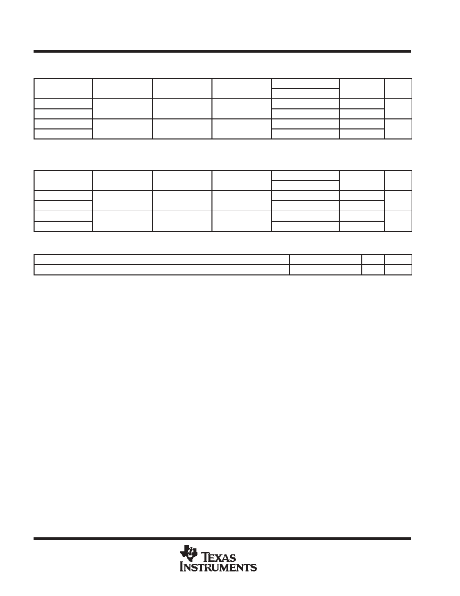
recommended operating conditions (see Note 3)
MIN
MAX
UNIT
VCC
Supply voltage
2
5.5
V
VCC = 2 V
1.5
VIH
High-level input voltage
VCC = 3 V
2.1
V
VIH
High-level input voltage
VCC = 5.5 V
3.85
V
VCC = 2 V
0.5
VIL
Low-level input voltage
VCC = 3 V
0.9
V
VIL
Low-level input voltage
VCC = 5.5 V
1.65
V
VI
Input voltage
0
5.5
V
VO
Output voltage
0
VCC
V
VCC = 2 V
-50
m
A
IOH
High-level output current
VCC = 3.3 V
±
0.3 V
-4
mA
IOH
High-level output current
VCC = 5 V
±
0.5 V
-8
mA
VCC = 2 V
50
m
A
IOL
Low-level output current
VCC = 3.3 V
±
0.3 V
4
mA
IOL
Low-level output current
VCC = 5 V
±
0.5 V
8
mA
t/
v
Input transition rise or fall rate
VCC = 3.3 V
±
0.3 V
100
ns/V
t/
v
Input transition rise or fall rate
VCC = 5 V
±
0.5 V
20
ns/V
TA
Operating free-air temperature
-40
85
∞
C
NOTE 3: All unused inputs of the device must be held at VCC or GND to ensure proper device operation. Refer to the TI application report,
Implications of Slow or Floating CMOS Inputs, literature number SCBA004.
electrical characteristics over recommended operating free-air temperature range (unless
otherwise noted)
PARAMETER
TEST CONDITIONS
VCC
TA = 25
∞
C
MIN
MAX
UNIT
PARAMETER
TEST CONDITIONS
VCC
MIN
TYP
MAX
MIN
MAX
UNIT
2 V
1.9
2
1.9
IOH = -50
m
A
3 V
2.9
3
2.9
VOH
IOH = -50
m
A
4.5 V
4.4
4.5
4.4
V
VOH
IOH = -4 mA
3 V
2.58
2.48
V
IOH = -8 mA
4.5 V
3.94
3.8
2 V
0.1
0.1
IOL = 50
m
A
3 V
0.1
0.1
VOL
IOL = 50
m
A
4.5 V
0.1
0.1
V
VOL
IOL = 4 mA
3 V
0.36
0.44
V
IOL = 8 mA
4.5 V
0.36
0.44
II
VI = 5.5 V or GND
0 V to 5.5 V
±
0.1
±
1
m
A
ICC
VI = VCC or GND,
IO = 0
5.5 V
1
10
m
A
Ci
VI = VCC or GND
5 V
4
10
10
pF
SN74AHC1G86
SINGLE 2 INPUT EXCLUSIVE OR GATE
SCLS323M - MARCH 1996 - REVISED JUNE 2005
4
POST OFFICE BOX 655303
∑
DALLAS, TEXAS 75265
switching characteristics over recommended operating free-air temperature range,
V
CC
= 3.3 V
±
0.3 V (unless otherwise noted) (see Figure 1)
PARAMETER
FROM
TO
LOAD
TA = 25
∞
C
MIN
MAX
UNIT
PARAMETER
FROM
(INPUT)
TO
(OUTPUT)
LOAD
CAPACITANCE
MIN
TYP
MAX
MIN
MAX
UNIT
tPLH
A or B
Y
CL = 15 pF
7
11
1
13
ns
tPHL
A or B
Y
CL = 15 pF
7
11
1
13
ns
tPLH
A or B
Y
CL = 50 pF
9.5
14.5
1
16.5
ns
tPHL
A or B
Y
CL = 50 pF
9.5
14.5
1
16.5
ns
switching characteristics over recommended operating free-air temperature range,
V
CC
= 5 V
±
0.5 V (unless otherwise noted) (see Figure 1)
PARAMETER
FROM
TO
LOAD
TA = 25
∞
C
MIN
MAX
UNIT
PARAMETER
FROM
(INPUT)
TO
(OUTPUT)
LOAD
CAPACITANCE
MIN
TYP
MAX
MIN
MAX
UNIT
tPLH
A or B
Y
CL = 15 pF
4.8
6.8
1
8
ns
tPHL
A or B
Y
CL = 15 pF
4.8
6.8
1
8
ns
tPLH
A or B
Y
CL = 50 pF
6.3
8.8
1
10
ns
tPHL
A or B
Y
CL = 50 pF
6.3
8.8
1
10
ns
operating characteristics, V
CC
= 5 V, T
A
= 25
∞
C
PARAMETER
TEST CONDITIONS
TYP
UNIT
Cpd
Power dissipation capacitance
No load,
f = 1 MHz
18
pF

SN74AHC1G86
SINGLE 2 INPUT EXCLUSIVE OR GATE
SCLS323M - MARCH 1996 - REVISED JUNE 2005
5
POST OFFICE BOX 655303
∑
DALLAS, TEXAS 75265
PARAMETER MEASUREMENT INFORMATION
50% VCC
VCC
VCC
0 V
0 V
th
tsu
VOLTAGE WAVEFORMS
SETUP AND HOLD TIMES
Data Input
tPLH
tPHL
tPHL
tPLH
VOH
VOH
VOL
VOL
VCC
0 V
50% VCC
50% VCC
Input
Out-of-Phase
Output
In-Phase
Output
Timing Input
50% VCC
VOLTAGE WAVEFORMS
PROPAGATION DELAY TIMES
INVERTING AND NONINVERTING OUTPUTS
Output
Control
Output
Waveform 1
S1 at VCC
(see Note B)
Output
Waveform 2
S1 at GND
(see Note B)
VOL
VOH
tPZL
tPZH
tPLZ
tPHZ
VCC
0 V
50% VCC
VOL
+ 0.3 V
50% VCC
0 V
VCC
VOLTAGE WAVEFORMS
ENABLE AND DISABLE TIMES
LOW- AND HIGH-LEVEL ENABLING
tPLH/tPHL
tPLZ/tPZL
tPHZ/tPZH
Open Drain
Open
VCC
GND
VCC
TEST
S1
VCC
0 V
50% VCC
tw
VOLTAGE WAVEFORMS
PULSE DURATION
Input
NOTES: A. CL includes probe and jig capacitance.
B. Waveform 1 is for an output with internal conditions such that the output is low, except when disabled by the output control.
Waveform 2 is for an output with internal conditions such that the output is high, except when disabled by the output control.
C. All input pulses are supplied by generators having the following characteristics: PRR
1 MHz, ZO = 50
, tr
3 ns, tf
3 ns.
D. The outputs are measured one at a time, with one input transition per measurement.
From Output
Under Test
CL
(see Note A)
LOAD CIRCUIT FOR
3-STATE AND OPEN-DRAIN OUTPUTS
S1
VCC
RL = 1 k
GND
From Output
Under Test
CL
(see Note A)
Test
Point
LOAD CIRCUIT FOR
TOTEM-POLE OUTPUTS
Open
50% VCC
50% VCC
50% VCC
50% VCC
50% VCC
50% VCC
50% VCC
50% VCC
VOH -
0.3 V
Figure 1. Load Circuit and Voltage Waveforms