Äîêóìåíòàöèÿ è îïèñàíèÿ www.docs.chipfind.ru
SN54AHC245, SN74AHC245
OCTAL BUS TRANSCEIVERS
WITH 3-STATE OUTPUTS
SCLS230I OCTOBER 1995 REVISED JULY 2003
1
POST OFFICE BOX 655303
·
DALLAS, TEXAS 75265
D
Operating Range 2-V to 5.5-V V
CC
D
Latch-Up Performance Exceeds 250 mA Per
JESD 17
description/ordering information
The 'AHC245 octal bus transceivers are designed
for asynchronous two-way communication
between data buses. The control-function
implementation minimizes external timing
requirements.
These devices allow data transmission from the
A bus to the B bus or from the B bus to the A bus,
depending on the logic level at the
direction-control (DIR) input. The output-enable
(OE) input can be used to disable the device so
that the buses are effectively isolated.
To ensure the high-impedance state during power
up or power down, OE should be tied to V
CC
through a pullup resistor; the minimum value of
the resistor is determined by the current-sinking
capability of the driver.
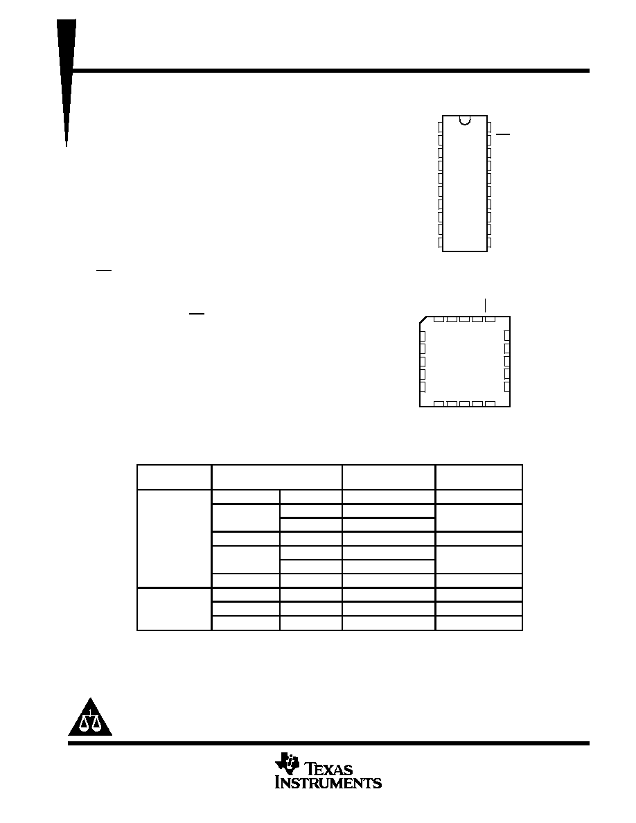
ORDERING INFORMATION
TA
PACKAGE
ORDERABLE
PART NUMBER
TOP-SIDE
MARKING
PDIP N
Tube
SN74AHC245N
SN74AHC245N
SOIC
DW
Tube
SN74AHC245DW
AHC245
SOIC DW
Tape and reel
SN74AHC245DWR
AHC245
40
°
C to 85
°
C
SSOP DB
Tape and reel
SN74AHC245DBR
HA245
TSSOP
PW
Tube
SN74AHC245PW
HA245
TSSOP PW
Tape and reel
SN74AHC245PWR
HA245
TVSOP DGV
Tape and reel
SN74AHC245DGVR
HA245
CDIP J
Tube
SNJ54AHC245J
SNJ54AHC245J
55
°
C to 125
°
C
CFP W
Tube
SNJ54AHC245W
SNJ54AHC245W
LCCC FK
Tube
SNJ54AHC245FK
SNJ54AHC245FK
Package drawings, standard packing quantities, thermal data, symbolization, and PCB design guidelines
are available at www.ti.com/sc/package.
Copyright
2003, Texas Instruments Incorporated
PRODUCTION DATA information is current as of publication date.
Products conform to specifications per the terms of Texas Instruments
standard warranty. Production processing does not necessarily include
testing of all parameters.
Please be aware that an important notice concerning availability, standard warranty, and use in critical applications of
Texas Instruments semiconductor products and disclaimers thereto appears at the end of this data sheet.
SN54AHC245 . . . J OR W PACKAGE
SN74AHC245 . . . DB, DGV, DW, N, OR PW PACKAGE
(TOP VIEW)
SN54AHC245 . . . FK PACKAGE
(TOP VIEW)
1
2
3
4
5
6
7
8
9
10
20
19
18
17
16
15
14
13
12
11
DIR
A1
A2
A3
A4
A5
A6
A7
A8
GND
V
CC
OE
B1
B2
B3
B4
B5
B6
B7
B8
3
2
1 20 19
9 10 11 12 13
4
5
6
7
8
18
17
16
15
14
B1
B2
B3
B4
B5
A3
A4
A5
A6
A7
A2
A1
DIR
B7
B6
OE
A8
GND
B8
V
CC
On products compliant to MIL-PRF-38535, all parameters are tested
unless otherwise noted. On all other products, production
processing does not necessarily include testing of all parameters.
SN54AHC245, SN74AHC245
OCTAL BUS TRANSCEIVERS
WITH 3-STATE OUTPUTS
SCLS230I OCTOBER 1995 REVISED JULY 2003
2
POST OFFICE BOX 655303
·
DALLAS, TEXAS 75265
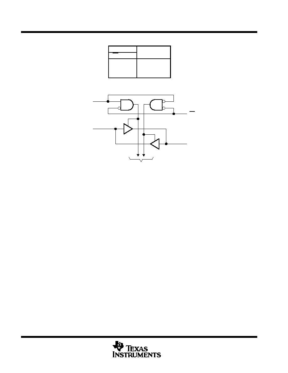
FUNCTION TABLE
(each transceiver)
INPUTS
OPERATION
OE
DIR
OPERATION
L
L
B data to A bus
L
H
A data to B bus
H
X
Isolation
logic diagram (positive logic)
DIR
OE
A1
B1
To Seven Other Channels
1
2
19
18
absolute maximum ratings over operating free-air temperature range (unless otherwise noted)
Supply voltage range, V
CC
0.5 V to 7 V
. . . . . . . . . . . . . . . . . . . . . . . . . . . . . . . . . . . . . . . . . . . . . . . . . . . . . . . . . .
Input voltage range, V
I
(see Note 1): Control inputs
0.5 V to 7 V
. . . . . . . . . . . . . . . . . . . . . . . . . . . . . . . . . . . .
I/O, Output voltage range, V
O
(see Note 1)
0.5 V to V
CC
+ 0.5 V
. . . . . . . . . . . . . . . . . . . . . . . . . . . . . . . . . . . . .
Input clamp current, I
IK
(V
I
< 0): Control inputs
20 mA
. . . . . . . . . . . . . . . . . . . . . . . . . . . . . . . . . . . . . . . . . . . . . .
I/O, Output clamp current, I
OK
(V
O
< 0 or V
O
> V
CC
)
±
20 mA
. . . . . . . . . . . . . . . . . . . . . . . . . . . . . . . . . . . . . . . .
Continuous output current, I
O
(V
O
= 0 to V
CC
)
±
25 mA
. . . . . . . . . . . . . . . . . . . . . . . . . . . . . . . . . . . . . . . . . . . . . .
Continuous current through V
CC
or GND
±
75 mA
. . . . . . . . . . . . . . . . . . . . . . . . . . . . . . . . . . . . . . . . . . . . . . . . . . .
Package thermal impedance,
JA
(see Note 2): DB package
70
°
C/W
. . . . . . . . . . . . . . . . . . . . . . . . . . . . . . . . .
DGV package
92
°
C/W
. . . . . . . . . . . . . . . . . . . . . . . . . . . . . . . .
DW package
58
°
C/W
. . . . . . . . . . . . . . . . . . . . . . . . . . . . . . . . .
N package
69
°
C/W
. . . . . . . . . . . . . . . . . . . . . . . . . . . . . . . . . . .
PW package
83
°
C/W
. . . . . . . . . . . . . . . . . . . . . . . . . . . . . . . . .
Storage temperature range, T
stg
65
°
C to 150
°
C
. . . . . . . . . . . . . . . . . . . . . . . . . . . . . . . . . . . . . . . . . . . . . . . . . . .
Stresses beyond those listed under "absolute maximum ratings" may cause permanent damage to the device. These are stress ratings only, and
functional operation of the device at these or any other conditions beyond those indicated under "recommended operating conditions" is not
implied. Exposure to absolute-maximum-rated conditions for extended periods may affect device reliability.
NOTES:
1. The input and output voltage ratings may be exceeded if the input and output current ratings are observed.
2. The package thermal impedance is calculated in accordance with JESD 51-7.
SN54AHC245, SN74AHC245
OCTAL BUS TRANSCEIVERS
WITH 3-STATE OUTPUTS
SCLS230I OCTOBER 1995 REVISED JULY 2003
3
POST OFFICE BOX 655303
·
DALLAS, TEXAS 75265
recommended operating conditions (see Note 3)
SN54AHC245
SN74AHC245
UNIT
MIN
MAX
MIN
MAX
UNIT
VCC
Supply voltage
2
5.5
2
5.5
V
VCC = 2 V
1.5
1.5
VIH
High-level input voltage
VCC = 3 V
2.1
2.1
V
VCC = 5.5 V
3.85
3.85
VCC = 2 V
0.5
0.5
VIL
Low-level input voltage
VCC = 3 V
0.9
0.9
V
VCC = 5.5 V
1.65
1.65
VI
Input voltage
OE or DIR
0
5.5
0
5.5
V
VO
Output voltage
A or B
0
VCC
0
VCC
V
VCC = 2 V
50
50
m
A
IOH
High-level output current
VCC = 3.3 V
±
0.3 V
4
4
mA
VCC = 5 V
±
0.5 V
8
8
mA
VCC = 2 V
50
50
m
A
IOL
Low-level output current
VCC = 3.3 V
±
0.3 V
4
4
mA
VCC = 5 V
±
0.5 V
8
8
mA
t
/
v
Input transition rise or fall rate
VCC = 3.3 V
±
0.3 V
100
100
ns/V
t
/
v
Input transition rise or fall rate
VCC = 5 V
±
0.5 V
20
20
ns/V
TA
Operating free-air temperature
55
125
40
85
°
C
NOTE 3: All unused inputs of the device must be held at VCC or GND to ensure proper device operation. Refer to the TI application report,
Implications of Slow or Floating CMOS Inputs, literature number SCBA004.
electrical characteristics over recommended operating free-air temperature range (unless
otherwise noted)
PARAMETER
TEST CONDITIONS
VCC
TA = 25
°
C
SN54AHC245
SN74AHC245
UNIT
PARAMETER
TEST CONDITIONS
VCC
MIN
TYP
MAX
MIN
MAX
MIN
MAX
UNIT
2 V
1.9
2
1.9
1.9
IOH = 50
m
A
3 V
2.9
3
2.9
2.9
VOH
4.5 V
4.4
4.5
4.4
4.4
V
IOH = 4 mA
3 V
2.58
2.48
2.48
IOH = 8 mA
4.5 V
3.94
3.8
3.8
2 V
0.1
0.1
0.1
IOL = 50
m
A
3 V
0.1
0.1
0.1
VOL
4.5 V
0.1
0.1
0.1
V
IOL = 4 mA
3 V
0.36
0.5
0.44
IOL = 8 mA
4.5 V
0.36
0.5
0.44
I
A or B inputs
V
V
or GND
5.5 V
±
0.1
±
1
±
1
A
II
OE or DIR
VI = VCC or GND
0 V to 5.5 V
±
0.1
±
1*
±
1
m
A
IOZ
VO = VCC or GND,
VI (OE) = VIL or VIH
5.5 V
±
0.25
±
2.5
±
2.5
m
A
ICC
VI = VCC or GND,
IO = 0
5.5 V
4
40
40
m
A
Ci
OE or DIR
VI = VCC or GND
5 V
2.5
10
10
pF
Cio
A or B inputs
VI = VCC or GND
5 V
4
pF
* On products compliant to MIL-PRF-38535, this parameter is not production tested at VCC = 0 V.
The parameter IOZ includes the input leakage current.
SN54AHC245, SN74AHC245
OCTAL BUS TRANSCEIVERS
WITH 3-STATE OUTPUTS
SCLS230I OCTOBER 1995 REVISED JULY 2003
4
POST OFFICE BOX 655303
·
DALLAS, TEXAS 75265
switching characteristics over recommended operating free-air temperature range,
V
CC
= 3.3 V
±
0.3 V (unless otherwise noted) (see Figure 1)
PARAMETER
FROM
TO
LOAD
TA = 25
°
C
SN54AHC245
SN74AHC245
UNIT
PARAMETER
(INPUT)
(OUTPUT)
CAPACITANCE
MIN
TYP
MAX
MIN
MAX
MIN
MAX
UNIT
tPLH
A or B
B or A
CL = 15 pF
5.8**
8.4**
1**
10**
1
10
ns
tPHL
A or B
B or A
CL = 15 pF
5.8**
8.4**
1**
10**
1
10
ns
tPZH
OE
A or B
CL = 15 pF
8.5**
13.2**
1**
15.5**
1
15.5
ns
tPZL
OE
A or B
CL = 15 pF
8.5**
13.2**
1**
15.5**
1
15.5
ns
tPHZ
OE
A or B
CL = 15 pF
8.9**
12.5**
1**
15.5**
1
15.5
ns
tPLZ
OE
A or B
CL = 15 pF
8.9**
12.5**
1**
15.5**
1
15.5
ns
tPLH
A or B
B or A
CL = 50 pF
8.3
11.9
1
13.5
1
13.5
ns
tPHL
A or B
B or A
CL = 50 pF
8.3
11.9
1
13.5
1
13.5
ns
tPZH
OE
A or B
CL = 50 pF
11
16.7
1
19
1
19
ns
tPZL
OE
A or B
CL = 50 pF
11
16.7
1
19
1
19
ns
tPHZ
OE
A or B
CL = 50 pF
11.5
15.8
1
18
1
18
ns
tPLZ
OE
A or B
CL = 50 pF
11.5
15.8
1
18
1
18
ns
tsk(o)
CL = 50 pF
1.5***
1.5
ns
** On products compliant to MIL-PRF-38535, this parameter is not production tested.
*** On products compliant to MIL-PRF-38535, this parameter does not apply.
switching characteristics over recommended operating free-air temperature range,
V
CC
= 5 V
±
0.5 V (unless otherwise noted) (see Figure 1)
PARAMETER
FROM
TO
LOAD
TA = 25
°
C
SN54AHC245
SN74AHC245
UNIT
PARAMETER
(INPUT)
(OUTPUT)
CAPACITANCE
MIN
TYP
MAX
MIN
MAX
MIN
MAX
UNIT
tPLH
A or B
B or A
CL = 15 pF
4*
5.5*
1*
6.5*
1
6.5
ns
tPHL
A or B
B or A
CL = 15 pF
4*
5.5*
1*
6.5*
1
6.5
ns
tPZH
OE
A or B
CL = 15 pF
5.8*
8.5*
1*
10*
1
10
ns
tPZL
OE
A or B
CL = 15 pF
5.8*
8.5*
1*
10*
1
10
ns
tPHZ
OE
A or B
CL = 15 pF
5.6*
7.8*
1*
9.2*
1
9.2
ns
tPLZ
OE
A or B
CL = 15 pF
5.6*
7.8*
1*
9.2*
1
9.2
ns
tPLH
A or B
B or A
CL = 50 pF
5.5
7.5
1
8.5
1
8.5
ns
tPHL
A or B
B or A
CL = 50 pF
5.5
7.5
1
8.5
1
8.5
ns
tPZH
OE
A or B
CL = 50 pF
7.3
10.6
1
12
1
12
ns
tPZL
OE
A or B
CL = 50 pF
7.3
10.6
1
12
1
12
ns
tPHZ
OE
A or B
CL = 50 pF
7
9.7
1
11
1
11
ns
tPLZ
OE
A or B
CL = 50 pF
7
9.7
1
11
1
11
ns
tsk(o)
CL = 50 pF
1**
1
ns
* On products compliant to MIL-PRF-38535, this parameter is not production tested.
** On products compliant to MIL-PRF-38535, this parameter does not apply.
SN54AHC245, SN74AHC245
OCTAL BUS TRANSCEIVERS
WITH 3-STATE OUTPUTS
SCLS230I OCTOBER 1995 REVISED JULY 2003
5
POST OFFICE BOX 655303
·
DALLAS, TEXAS 75265
noise characteristics, V
CC
= 5 V, C
L
= 50 pF, T
A
= 25
°
C (see Note 4)
PARAMETER
SN74AHC245
UNIT
PARAMETER
MIN
TYP
MAX
UNIT
VOL(P)
Quiet output, maximum dynamic VOL
0.9
V
VOL(V)
Quiet output, minimum dynamic VOL
0.9
V
VOH(V)
Quiet output, minimum dynamic VOH
4.3
V
VIH(D)
High-level dynamic input voltage
3.5
V
VIL(D)
Low-level dynamic input voltage
1.5
V
NOTE 4: Characteristics are for surface-mount packages only.
operating characteristics, V
CC
= 5 V, T
A
= 25
°
C
PARAMETER
TEST CONDITIONS
TYP
UNIT
Cpd
Power dissipation capacitance
No load,
f = 1 MHz
14
pF