
Please be aware that an important notice concerning availability, standard warranty, and use in critical applications of
Texas Instruments semiconductor products and disclaimers thereto appears at the end of this data sheet.
SN74ALVCH16244
16 BIT BUFFER/DRIVER
WITH 3 STATE OUTPUTS
SCES014I - JULY 1995 - REVISED AUGUST 2003
1
POST OFFICE BOX 655303
∑
DALLAS, TEXAS 75265
D
Member of the Texas Instruments
Widebus
Family
D
Operates From 1.65 V to 3.6 V
D
Max t
pd
of 3 ns at 3.3 V
D
±
24-mA Output Drive at 3.3 V
D
Bus Hold on Data Inputs Eliminates the
Need for External Pullup/Pulldown
Resistors
D
Latch-Up Performance Exceeds 250 mA Per
JESD 17
D
ESD Protection Exceeds JESD 22
- 2000-V Human-Body Model (A114-A)
- 200-V Machine Model (A115-A)
description/ordering information
This 16-bit buffer/driver is designed for 1.65-V to
3.6-V V
CC
operation.
The SN74ALVCH16244 is designed specifically
to improve the performance and density of 3-state
memory address drivers, clock drivers, and
bus-oriented receivers and transmitters.
The device can be used as four 4-bit buffers, two
8-bit buffers, or one 16-bit buffer. It provides true
outputs and symmetrical active-low
output-enable (OE) inputs.
To ensure the high-impedance state during power up or power down, OE should be tied to V
CC
through a pullup
resistor; the minimum value of the resistor is determined by the current-sinking capability of the driver.
Active bus-hold circuitry holds unused or undriven inputs at a valid logic state. Use of pullup or pulldown resistors
with the bus-hold circuitry is not recommended.
ORDERING INFORMATION
TA
PACKAGE
ORDERABLE
PART NUMBER
TOP-SIDE
MARKING
SSOP - DL
Tube
SN74ALVCH16244DL
ALVCH16244
SSOP - DL
Tape and reel
SN74ALVCH16244DLR
ALVCH16244
-40
∞
C to 85
∞
C
TSSOP - DGG
Tape and reel
SN74ALVCH16244DGGR
ALVCH16244
-40
∞
C to 85
∞
C
TVSOP - DGV
Tape and reel
SN74ALVCH16244DGVR
VH244
VFBGA - GQL
Tape and reel
SN74ALVCH16244KR
VH244
VFBGA - ZQL (Pb-free)
Tape and reel
74ALVCH16244ZQLR
VH244
Package drawings, standard packing quantities, thermal data, symbolization, and PCB design guidelines are
available at www.ti.com/sc/package.
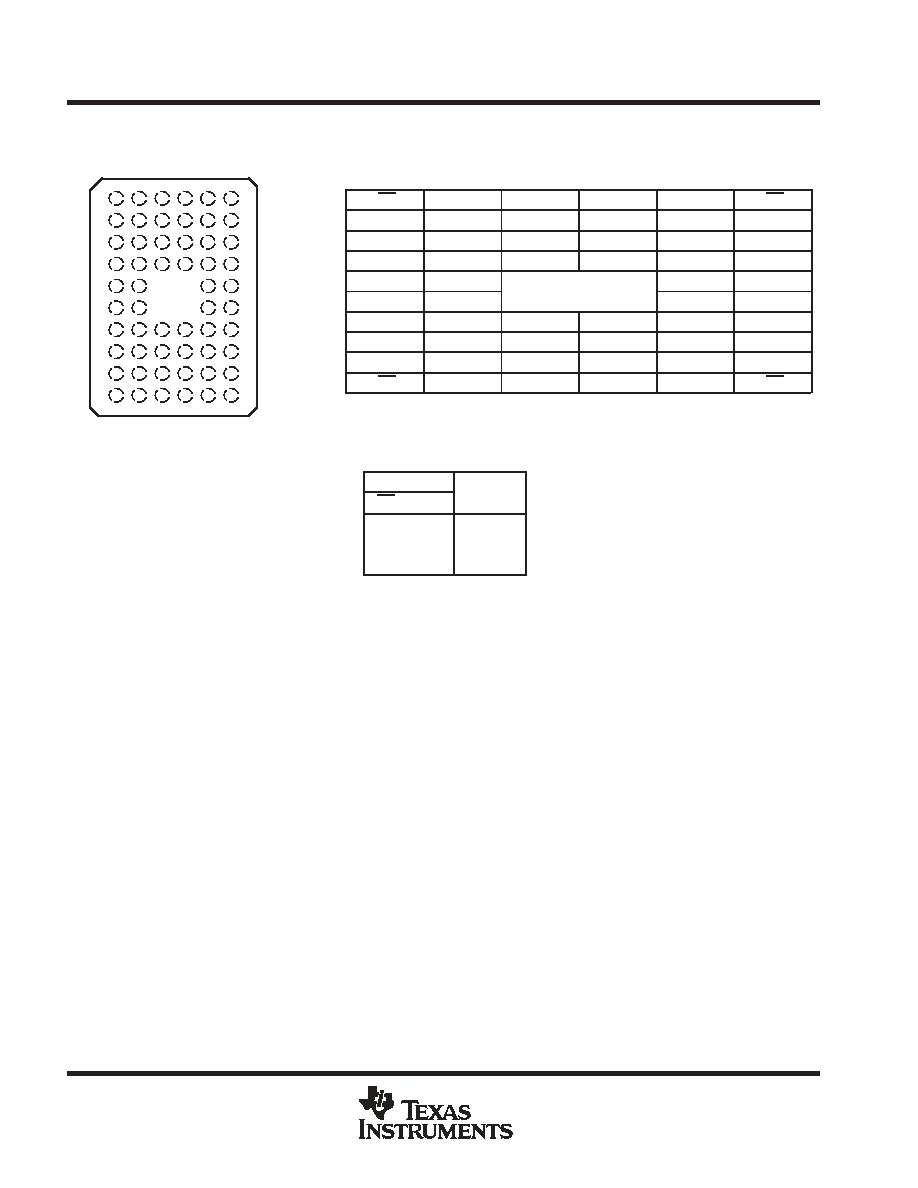
DGG, DGV, OR DL PACKAGE
(TOP VIEW)
1
2
3
4
5
6
7
8
9
10
11
12
13
14
15
16
17
18
19
20
21
22
23
24
48
47
46
45
44
43
42
41
40
39
38
37
36
35
34
33
32
31
30
29
28
27
26
25
1OE
1Y1
1Y2
GND
1Y3
1Y4
V
CC
2Y1
2Y2
GND
2Y3
2Y4
3Y1
3Y2
GND
3Y3
3Y4
V
CC
4Y1
4Y2
GND
4Y3
4Y4
4OE
2OE
1A1
1A2
GND
1A3
1A4
V
CC
2A1
2A2
GND
2A3
2A4
3A1
3A2
GND
3A3
3A4
V
CC
4A1
4A2
GND
4A3
4A4
3OE
PRODUCTION DATA information is current as of publication date.
Products conform to specifications per the terms of Texas Instruments
standard warranty. Production processing does not necessarily include
testing of all parameters.
Copyright
2003, Texas Instruments Incorporated
Widebus is a trademark of Texas Instruments.
SN74ALVCH16244
16 BIT BUFFER/DRIVER
WITH 3 STATE OUTPUTS
SCES014I - JULY 1995 - REVISED AUGUST 2003
2
POST OFFICE BOX 655303
∑
DALLAS, TEXAS 75265
terminal assignments
1
2
3
4
5
6
A
1OE
NC
NC
NC
NC
2OE
B
1Y2
1Y1
GND
GND
1A1
1A2
C
1Y4
1Y3
VCC
VCC
1A3
1A4
D
2Y2
2Y1
GND
GND
2A1
2A2
E
2Y4
2Y3
2A3
2A4
F
3Y1
3Y2
3A2
3A1
G
3Y3
3Y4
GND
GND
3A4
3A3
H
4Y1
4Y2
VCC
VCC
4A2
4A1
J
4Y3
4Y4
GND
GND
4A4
4A3
K
4OE
NC
NC
NC
NC
3OE
NC - No internal connection
FUNCTION TABLE
(each 4-bit buffer)
INPUTS
OUTPUT
OE
A
OUTPUT
Y
L
H
H
L
L
L
H
X
Z
GQL OR ZQL PACKAGE
(TOP VIEW)
J
H
G
F
E
D
C
B
A
2
1
3
4
6
5
K

SN74ALVCH16244
16 BIT BUFFER/DRIVER
WITH 3 STATE OUTPUTS
SCES014I - JULY 1995 - REVISED AUGUST 2003
3
POST OFFICE BOX 655303
∑
DALLAS, TEXAS 75265
logic diagram (positive logic)
1OE
1A1
1A2
1A3
1A4
1Y1
1Y2
1Y3
1Y4
1
47
46
44
43
2
3
5
6
2OE
2A1
2A2
2A3
2A4
2Y1
2Y2
2Y3
2Y4
48
41
40
38
37
8
9
11
12
3OE
3A1
3A2
3A3
3A4
3Y1
3Y2
3Y3
3Y4
25
36
35
33
32
13
14
16
17
4OE
4A1
4A2
4A3
4A4
4Y1
4Y2
4Y3
4Y4
24
30
29
27
26
19
20
22
23
Pin numbers shown are for the DGG, DGV, and DL packages.
absolute maximum ratings over operating free-air temperature range (unless otherwise noted)
Supply voltage range, V
CC
-0.5 V to 4.6 V
. . . . . . . . . . . . . . . . . . . . . . . . . . . . . . . . . . . . . . . . . . . . . . . . . . . . . . . . .
Input voltage range, V
I
(see Note 1)
-0.5 V to 4.6 V
. . . . . . . . . . . . . . . . . . . . . . . . . . . . . . . . . . . . . . . . . . . . . . . . .
Output voltage range, V
O
(see Notes 1 and 2)
-0.5 V to V
CC
+ 0.5 V
. . . . . . . . . . . . . . . . . . . . . . . . . . . . . . . . . .
Input clamp current, I
IK
(V
I
< 0)
-50 mA
. . . . . . . . . . . . . . . . . . . . . . . . . . . . . . . . . . . . . . . . . . . . . . . . . . . . . . . . . . .
Output clamp current, I
OK
(V
O
< 0)
-50 mA
. . . . . . . . . . . . . . . . . . . . . . . . . . . . . . . . . . . . . . . . . . . . . . . . . . . . . . . .
Continuous output current, I
O
±
50 mA
. . . . . . . . . . . . . . . . . . . . . . . . . . . . . . . . . . . . . . . . . . . . . . . . . . . . . . . . . . . . .
Continuous current through each V
CC
or GND
±
100 mA
. . . . . . . . . . . . . . . . . . . . . . . . . . . . . . . . . . . . . . . . . . . . .
Package thermal impedance,
JA
(see Note 3): DGG package
70
∞
C/W
. . . . . . . . . . . . . . . . . . . . . . . . . . . . . . .
DGV package
58
∞
C/W
. . . . . . . . . . . . . . . . . . . . . . . . . . . . . . . .
DL package
63
∞
C/W
. . . . . . . . . . . . . . . . . . . . . . . . . . . . . . . . .
GQL/ZQL package
42
∞
C/W
. . . . . . . . . . . . . . . . . . . . . . . . . . .
Storage temperature range, T
stg
-65
∞
C to 150
∞
C
. . . . . . . . . . . . . . . . . . . . . . . . . . . . . . . . . . . . . . . . . . . . . . . . . . .
Stresses beyond those listed under "absolute maximum ratings" may cause permanent damage to the device. These are stress ratings only, and
functional operation of the device at these or any other conditions beyond those indicated under "recommended operating conditions" is not
implied. Exposure to absolute-maximum-rated conditions for extended periods may affect device reliability.
NOTES:
1. The input negative-voltage and output voltage ratings may be exceeded if the input and output current ratings are observed.
2. This value is limited to 4.6 V maximum.
3. The package thermal impedance is calculated in accordance with JESD 51-7.

SN74ALVCH16244
16 BIT BUFFER/DRIVER
WITH 3 STATE OUTPUTS
SCES014I - JULY 1995 - REVISED AUGUST 2003
4
POST OFFICE BOX 655303
∑
DALLAS, TEXAS 75265
recommended operating conditions (see Note 4)
MIN
MAX
UNIT
VCC
Supply voltage
1.65
3.6
V
VCC = 1.65 V to 1.95 V
0.65
◊
VCC
VIH
High-level input voltage
VCC = 2.3 V to 2.7 V
1.7
V
VIH
High-level input voltage
VCC = 2.7 V to 3.6 V
2
V
VCC = 1.65 V to 1.95 V
0.35
◊
VCC
VIL
Low-level input voltage
VCC = 2.3 V to 2.7 V
0.7
V
VIL
Low-level input voltage
VCC = 2.7 V to 3.6 V
0.8
V
VI
Input voltage
0
VCC
V
VO
Output voltage
0
VCC
V
VCC = 1.65 V
-4
IOH
High-level output current
VCC = 2.3 V
-12
mA
IOH
High-level output current
VCC = 2.7 V
-12
mA
VCC = 3 V
-24
VCC = 1.65 V
4
IOL
Low-level output current
VCC = 2.3 V
12
mA
IOL
Low-level output current
VCC = 2.7 V
12
mA
VCC = 3 V
24
t/
v
Input transition rise or fall rate
10
ns/V
TA
Operating free-air temperature
-40
85
∞
C
NOTE 4: All unused control inputs of the device must be held at VCC or GND to ensure proper device operation. Refer to the TI application report,
Implications of Slow or Floating CMOS Inputs, literature number SCBA004.

SN74ALVCH16244
16 BIT BUFFER/DRIVER
WITH 3 STATE OUTPUTS
SCES014I - JULY 1995 - REVISED AUGUST 2003
5
POST OFFICE BOX 655303
∑
DALLAS, TEXAS 75265
electrical characteristics over recommended operating free-air temperature range (unless
otherwise noted)
PARAMETER
TEST CONDITIONS
VCC
MIN
TYP
MAX
UNIT
IOH = -100
µ
A
1.65 V to 3.6 V
VCC-0.2
IOH = -4 mA
1.65 V
1.2
IOH = -6 mA
2.3 V
2
VOH
2.3 V
1.7
V
VOH
IOH = -12 mA
2.7 V
2.2
V
IOH = -12 mA
3 V
2.4
IOH = -24 mA
3 V
2
IOL = 100
µ
A
1.65 V to 3.6 V
0.2
IOL = 4 mA
1.65 V
0.45
VOL
IOL = 6 mA
2.3 V
0.4
V
VOL
IOL = 12 mA
2.3 V
0.7
V
IOL = 12 mA
2.7 V
0.4
IOL = 24 mA
3 V
0.55
II
VI = VCC or GND
3.6 V
±
5
µ
A
VI = 0.58 V
1.65 V
25
VI = 1.07 V
1.65 V
-25
VI = 0.7 V
2.3 V
45
II(hold)
VI = 1.7 V
2.3 V
-45
µ
A
II(hold)
VI = 0.8 V
3 V
75
µ
A
VI = 2 V
3 V
-75
VI = 0 to 3.6 V
3.6 V
±
500
IOZ
VO = VCC or GND
3.6 V
±
10
µ
A
ICC
VI = VCC or GND,
IO = 0
3.6 V
40
µ
A
ICC
One input at VCC - 0.6 V,
Other inputs at VCC or GND
3 V to 3.6 V
750
µ
A
Ci
Control inputs
VI = VCC or GND
3.3 V
3
pF
Ci
Data inputs
VI = VCC or GND
3.3 V
6
pF
Co
Outputs
VO = VCC or GND
3.3 V
7
pF
All typical values are at VCC = 3.3 V, TA = 25
∞
C.
This is the bus-hold maximum dynamic current. It is the minimum overdrive current required to switch the input from one state to another.
switching characteristics over recommended operating free-air temperature range (unless
otherwise noted) (see Figure 1)
PARAMETER
FROM
(INPUT)
TO
(OUTPUT)
VCC = 1.8 V
VCC = 2.5 V
±
0.2 V
VCC = 2.7 V
VCC = 3.3 V
±
0.3 V
UNIT
PARAMETER
(INPUT)
(OUTPUT)
TYP
MIN
MAX
MIN
MAX
MIN
MAX
UNIT
tpd
A
Y
ß
1
3.7
3.6
1
3
ns
ten
OE
Y
ß
1
5.7
5.4
1
4.4
ns
tdis
OE
Y
ß
1
5.2
4.6
1
4.1
ns
ß This information was not available at the time of publication.