
SN74ALVCH16646
16-BIT BUS TRANSCEIVER AND REGISTER
WITH 3-STATE OUTPUTS
SCES032E≠ JULY 1995 ≠ REVISED FEBRUARY 1999
1
POST OFFICE BOX 655303
∑
DALLAS, TEXAS 75265
D
Member of the Texas Instruments
Widebus
TM
Family
D
EPIC
TM
(Enhanced-Performance Implanted
CMOS) Submicron Process
D
ESD Protection Exceeds 2000 V Per
MIL-STD-883, Method 3015; Exceeds 200 V
Using Machine Model (C = 200 pF, R = 0)
D
Latch-Up Performance Exceeds 250 mA Per
JESD 17
D
Bus Hold on Data Inputs Eliminates the
Need for External Pullup/Pulldown
Resistors
D
Package Options Include Plastic 300-mil
Shrink Small-Outline (DL), Thin Shrink
Small-Outline (DGG), and Thin Very
Small-Outline (DGV) Packages
description
This 16-bit bus transceiver and register is
designed for 1.65-V to 3.6-V V
CC
operation.
The SN74ALVCH16646 can be used as two 8-bit
transceivers or one 16-bit transceiver. Data on the
A or B bus is clocked into the registers on the
low-to-high transition of the appropriate clock
(CLKAB or CLKBA) input. Figure 1 illustrates the
four fundamental bus-management functions that
can be performed with the SN74ALVCH16646.
Output-enable (OE) and direction-control (DIR)
inputs are provided to control the transceiver
functions. In the transceiver mode, data present at
the high-impedance port may be stored in either
register or in both. The select-control (SAB and SBA) inputs can multiplex stored and real-time (transparent
mode) data. The circuitry used for select control eliminates the typical decoding glitch that occurs in a multiplexer
during the transition between stored and real-time data. DIR determines which bus receives data when OE is
low. In the isolation mode (OE high), A data may be stored in one register and/or B data may be stored in the
other register.
When an output function is disabled, the input function is still enabled and may be used to store and transmit
data. Only one of the two buses, A or B, can be driven at a time.
To ensure the high-impedance state during power up or power down, OE should be tied to V
CC
through a pullup
resistor; the minimum value of the resistor is determined by the current-sinking capability of the driver.
Active bus-hold circuitry is provided to hold unused or floating data inputs at a valid logic level.
The SN74ALVCH16646 is characterized for operation from ≠40
∞
C to 85
∞
C.
PRODUCTION DATA information is current as of publication date.
Products conform to specifications per the terms of Texas Instruments
standard warranty. Production processing does not necessarily include
testing of all parameters.
Please be aware that an important notice concerning availability, standard warranty, and use in critical applications of
Texas Instruments semiconductor products and disclaimers thereto appears at the end of this data sheet.
DGG, DGV, OR DL PACKAGE
(TOP VIEW)
1
2
3
4
5
6
7
8
9
10
11
12
13
14
15
16
17
18
19
20
21
22
23
24
25
26
27
28
56
55
54
53
52
51
50
49
48
47
46
45
44
43
42
41
40
39
38
37
36
35
34
33
32
31
30
29
1DIR
1CLKAB
1SAB
GND
1A1
1A2
V
CC
1A3
1A4
1A5
GND
1A6
1A7
1A8
2A1
2A2
2A3
GND
2A4
2A5
2A6
V
CC
2A7
2A8
GND
2SAB
2CLKAB
2DIR
1OE
1CLKBA
1SBA
GND
1B1
1B2
V
CC
1B3
1B4
1B5
GND
1B6
1B7
1B8
2B1
2B2
2B3
GND
2B4
2B5
2B6
V
CC
2B7
2B8
GND
2SBA
2CLKBA
2OE
EPIC and Widebus are trademarks of Texas Instruments Incorporated.
Copyright
©
1999, Texas Instruments Incorporated
SN74ALVCH16646
16-BIT BUS TRANSCEIVER AND REGISTER
WITH 3-STATE OUTPUTS
SCES032E≠ JULY 1995 ≠ REVISED FEBRUARY 1999
2
POST OFFICE BOX 655303
∑
DALLAS, TEXAS 75265
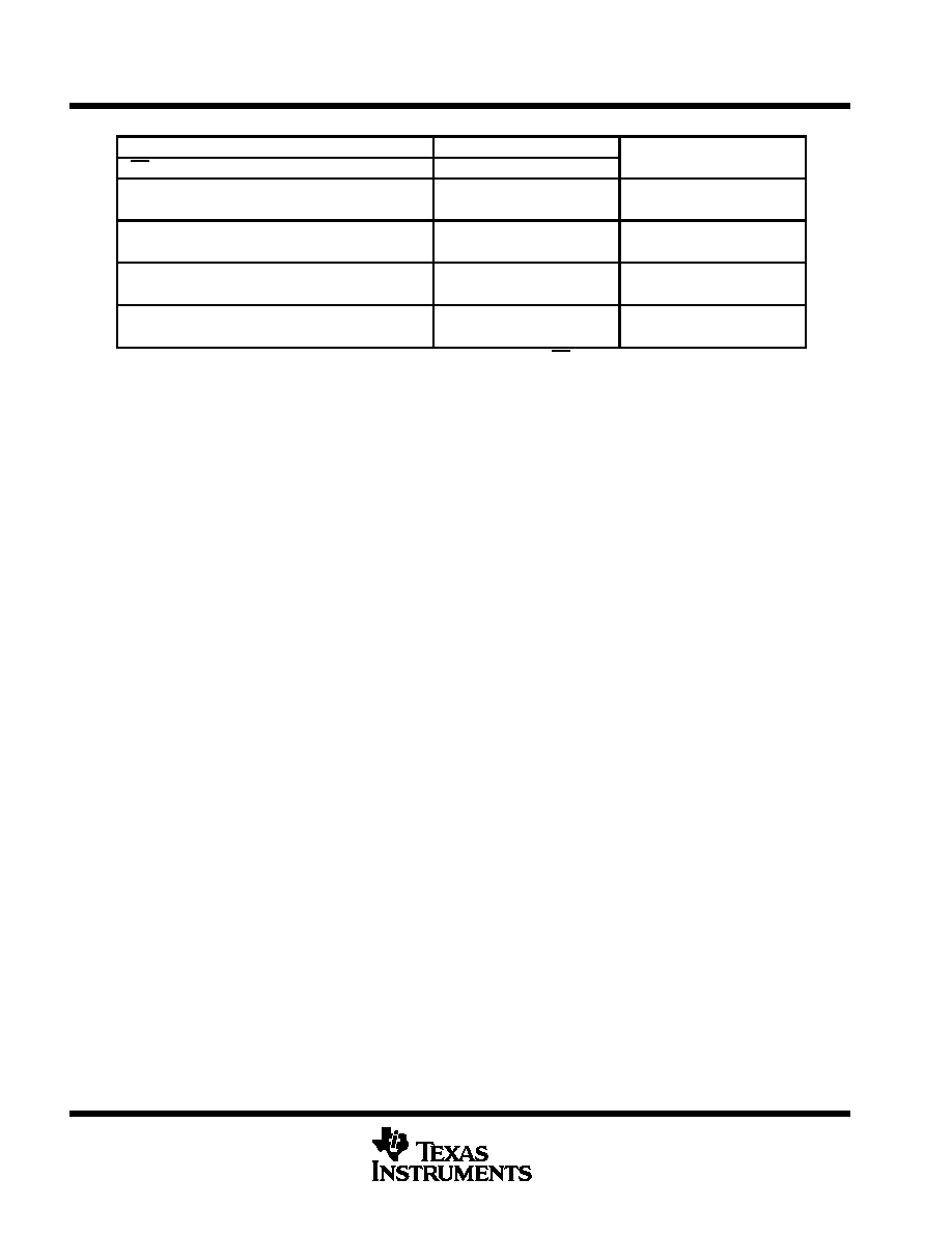
FUNCTION TABLE
INPUTS
DATA I/Os
OPERATION OR FUNCTION
OE
DIR
CLKAB
CLKBA
SAB
SBA
A1≠A8
B1≠B8
OPERATION OR FUNCTION
X
X
X
X
X
Input
Unspecified
Store A, B unspecified
X
X
X
X
X
Unspecified
Input
Store B, A unspecified
H
X
X
X
Input
Input
Store A and B data
H
X
H or L
H or L
X
X
Input disabled
Input disabled
Isolation, hold storage
L
L
X
X
X
L
Output
Input
Real-time B data to A bus
L
L
X
H or L
X
H
Output
Input
Stored B data to A bus
L
H
X
X
L
X
Input
Output
Real-time A data to B bus
L
H
H or L
X
H
X
Input
Output
Stored A data to B bus
The data-output functions may be enabled or disabled by various signals at OE and DIR. Data-input functions always are
enabled; i.e., data at the bus terminals is stored on every low-to-high transition of the clock inputs.


