
www.ti.com
FEATURES
DGG, DGV, OR DL PACKAGE
(TOP VIEW)
1
2
3
4
5
6
7
8
9
10
11
12
13
14
15
16
17
18
19
20
21
22
23
24
25
26
27
28
56
55
54
53
52
51
50
49
48
47
46
45
44
43
42
41
40
39
38
37
36
35
34
33
32
31
30
29
OEA
OEB1
2B3
GND
2B2
2B1
V
CC
A1
A2
A3
GND
A4
A5
A6
A7
A8
A9
GND
A10
A11
A12
V
CC
1B1
1B2
GND
1B3
NC
SEL
OEB2
CLKENA2
2B4
GND
2B5
2B6
V
CC
2B7
2B8
2B9
GND
2B10
2B11
2B12
1B12
1B11
1B10
GND
1B9
1B8
1B7
V
CC
1B6
1B5
GND
1B4
CLKENA1
CLK
NC - No internal connection
SN74ALVCHR16269A
12-BIT TO 24-BIT REGISTERED BUS EXCHANGER
WITH 3-STATE OUTPUTS
SCES050O ≠ AUGUST 1995 ≠ REVISED SEPTEMBER 2004
∑
Member of the Texas Instruments WidebusTM
Family
∑
Operates From 1.65 V to 3.6 V
∑
Max t
pd
of 5.2 ns at 3.3 V
∑
±
24-mA Output Drive at 3.3 V
∑
All Outputs Have Equivalent 26-
Series
Resistors, So No External Resistors Are
Required
∑
Bus Hold on Data Inputs Eliminates the Need
for External Pullup/Pulldown Resistors
∑
Latch-Up Performance Exceeds 250 mA Per
JESD 17
∑
ESD Protection Exceeds JESD 22
≠ 2000-V Human-Body Model (A114-A)
≠ 200-V Machine Model (A115-A)
DESCRIPTION/ORDERING INFORMATION
This 12-bit to 24-bit registered bus exchanger is
designed for 1.65-V to 3.6-V V
CC
operation.
The SN74ALVCHR16269A is used in applications in
which two ports must be multiplexed onto, or
demultiplexed from, a single port. It is particularly
suitable
as
an
interface
between
synchronous
DRAMs and high-speed microprocessors.
Data is stored in the internal B-port registers on the
low-to-high transition of the clock (CLK) input, when
the appropriate clock-enable (CLKENA) inputs are
low. Proper control of these inputs allows two
sequential 12-bit words to be presented as a 24-bit
word on the B port. For data transfer in the B-to-A
direction, a single storage register is provided. The select (SEL) line selects 1B or 2B data for the A outputs. The
register on the A output permits the fastest possible data transfer, thus extending the period during which the
data is valid on the bus. The control terminals are registered so that all transactions are synchronous with CLK.
Data flow is controlled by the active-low output enables (OEA, OEB1, and OEB2).
ORDERING INFORMATION
T
A
PACKAGE
(1)
ORDERABLE PART NUMBER
TOP-SIDE MARKING
Tube
SN74ALVCHR16269AL
SSOP ≠ DL
ALVCHR16269A
Tape and reel
SN74ALVCHR16269ALR
-40
∞
C to 85
∞
C
TSSOP ≠ DGG
Tape and reel
SN74ALVCHR16269AGR
ALVCHR16269A
TVSOP ≠ DGV
Tape and reel
SN74ALVCHR16269AVR
VR269A
(1)
Package drawings, standard packing quantities, thermal data, symbolization, and PCB design guidelines are available at
www.ti.com/sc/package.
Please be aware that an important notice concerning availability, standard warranty, and use in critical applications of Texas
Instruments semiconductor products and disclaimers thereto appears at the end of this data sheet.
Widebus is a trademark of Texas Instruments.
PRODUCTION DATA information is current as of publication date.
Copyright © 1995≠2004, Texas Instruments Incorporated
Products conform to specifications per the terms of the Texas
Instruments standard warranty. Production processing does not
necessarily include testing of all parameters.

www.ti.com
DESCRIPTION/ORDERING INFORMATION (CONTINUED)
FUNCTION TABLES
SN74ALVCHR16269A
12-BIT TO 24-BIT REGISTERED BUS EXCHANGER
WITH 3-STATE OUTPUTS
SCES050O ≠ AUGUST 1995 ≠ REVISED SEPTEMBER 2004
To ensure the high-impedance state during power up or power down, a clock pulse should be applied as soon as
possible, and OE should be tied to V
CC
through a pullup resistor; the minimum value of the resistor is determined
by the current-sinking capability of the driver. Due to OE being routed through a register, the active state of the
outputs cannot be determined prior to the arrival of the first clock pulse.
Active bus-hold circuitry holds unused or undriven inputs at a valid logic state. Use of pullup or pulldown resistors
with the bus-hold circuitry is not recommended.
All outputs are designed to sink up to 12 mA and include equivalent 26-
resistors to reduce overshoot and
undershoot.
OUTPUT ENABLE
INPUTS
OUTPUTS
CLK
OEA
OEB
A
1B, 2B
H
H
Z
Z
H
L
Z
Active
L
H
Active
Z
L
L
Active
Active
A-TO-B STORAGE (OEB = L)
INPUTS
OUTPUTS
CLKENA1
CLKENA2
CLK
A
1B
2B
L
H
L
L
2B
0
(1)
L
H
H
H
2B
0
(1)
L
L
L
L
L
L
L
H
H
H
H
L
L
1B
0
(1)
L
H
L
H
1B
0
(1)
H
H
H
X
X
1B
0
(1)
2B
0
(1)
(1)
Output level before the indicated steady-state input conditions were
established
B-TO-A STORAGE (OEA = L)
INPUTS
OUTPUT
A
CLK
SEL
1B
2B
X
H
X
X
A
0
(1)
X
L
X
X
A
0
(1)
H
L
X
L
H
H
X
H
L
X
L
L
L
X
H
H
(1)
Output level before the indicated steady-state input conditions were
established
2
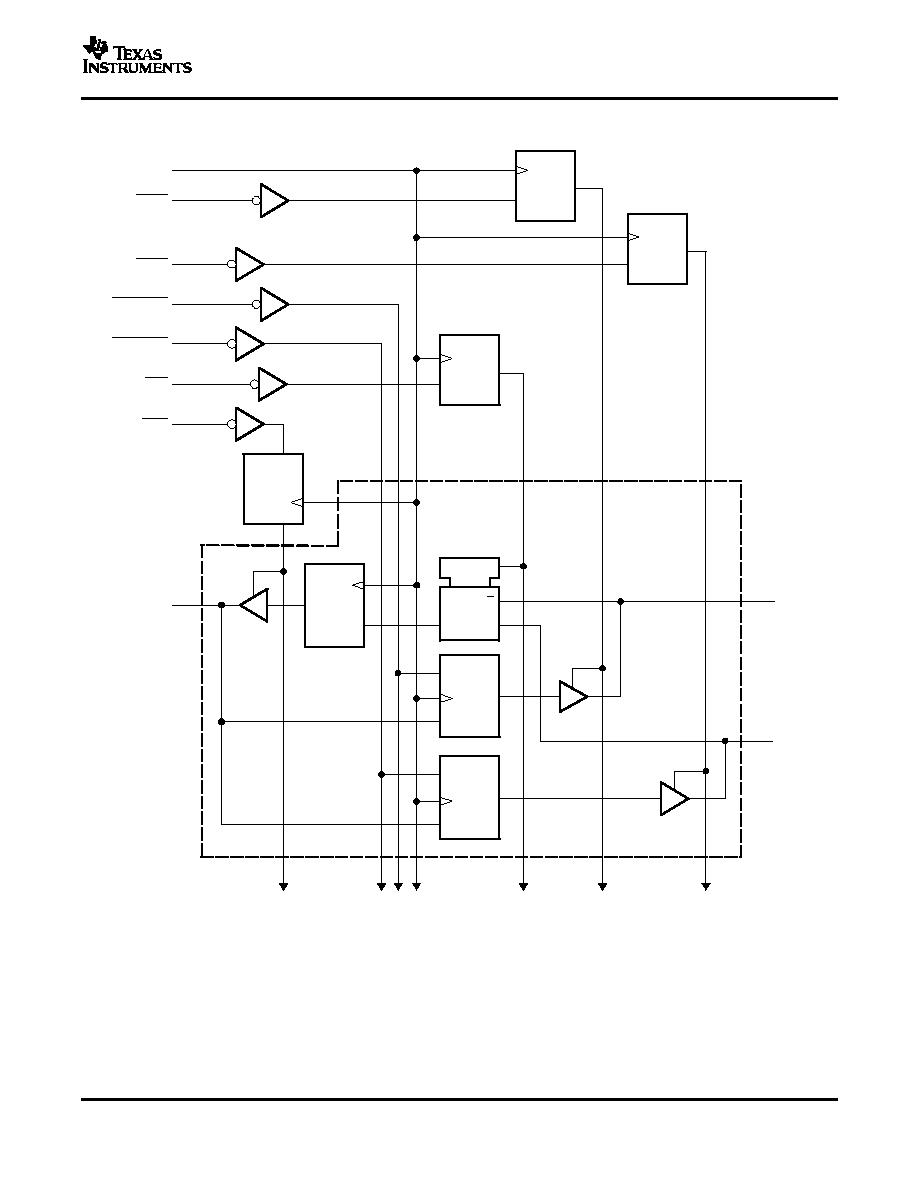
www.ti.com
CLK
SEL
A1
1B1
2B1
CLKENA1
CLKENA2
1D
CE
1D
CE
G1
1
1
OEA
1D
C1
1 of 12 Channels
OEB1
OEB2
1D
1D
C1
C1
C1
C1
1D
C1
1D
C1
29
2
56
30
55
28
1
8
23
6
SN74ALVCHR16269A
12-BIT TO 24-BIT REGISTERED BUS EXCHANGER
WITH 3-STATE OUTPUTS
SCES050O ≠ AUGUST 1995 ≠ REVISED SEPTEMBER 2004
LOGIC DIAGRAM (POSITIVE LOGIC)
3

www.ti.com
ABSOLUTE MAXIMUM RATINGS
(1)
RECOMMENDED OPERATING CONDITIONS
(1)
SN74ALVCHR16269A
12-BIT TO 24-BIT REGISTERED BUS EXCHANGER
WITH 3-STATE OUTPUTS
SCES050O ≠ AUGUST 1995 ≠ REVISED SEPTEMBER 2004
over operating free-air temperature range (unless otherwise noted)
MIN
MAX
UNIT
V
CC
Supply voltage range
-0.5
4.6
V
Except I/O ports
(2)
-0.5
4.6
V
I
Input voltage range
V
I/O ports
(2) (3)
-0.5
V
CC
+ 0.5
V
O
Output voltage range
(2) (3)
V
CC
+ 0.5
V
I
IK
Input clamp current
V
I
< 0
-50
mA
I
OK
Output clamp current
V
O
< 0
-50
mA
I
O
Continuous output current
±
50
mA
Continuous current through each V
CC
or GND
±
100
mA
DGG package
64
JA
Package thermal impedance
(4)
DGV package
48
∞
C/W
DL package
56
T
stg
Storage temperature range
-65
150
∞
C
(1)
Stresses beyond those listed under "absolute maximum ratings" may cause permanent damage to the device. These are stress ratings
only, and functional operation of the device at these or any other conditions beyond those indicated under "recommended operating
conditions" is not implied. Exposure to absolute-maximum-rated conditions for extended periods may affect device reliability.
(2)
The input negative-voltage and output voltage ratings may be exceeded if the input and output current ratings are observed.
(3)
This value is limited to 4.6 V, maximum.
(4)
The package thermal impedance is calculated in accordance with JESD 51-7.
MIN
MAX
UNIT
V
CC
Supply voltage
1.65
3.6
V
V
CC
= 1.65 V to 1.95 V
0.65
◊
V
CC
V
IH
High-level input voltage
V
CC
= 2.3 V to 2.7 V
1.7
V
V
CC
= 2.7 V to 3.6 V
2
V
CC
= 1.65 V to 1.95 V
0.35
◊
V
CC
V
IL
Low-level input voltage
V
CC
= 2.3 V to 2.7 V
0.7
V
V
CC
= 2.7 V to 3.6 V
0.8
V
I
Input voltage
0
V
CC
V
V
O
Output voltage
0
V
CC
V
V
CC
= 1.65 V
-2
V
CC
= 2.3 V
-6
I
OH
High-level output current
mA
V
CC
= 2.7 V
-8
V
CC
= 3 V
-12
V
CC
= 1.65 V
2
V
CC
= 2.3 V
6
I
OL
Low-level output current
mA
V
CC
= 2.7 V
8
V
CC
= 3 V
12
t/
v
Input transition rise or fall rate
10
ns/V
T
A
Operating free-air temperature
-40
85
∞
C
(1)
All unused control inputs of the device must be held at V
CC
or GND to ensure proper device operation. Refer to the TI application report,
Implications of Slow or Floating CMOS Inputs, literature number SCBA004.
4

www.ti.com
ELECTRICAL CHARACTERISTICS
SN74ALVCHR16269A
12-BIT TO 24-BIT REGISTERED BUS EXCHANGER
WITH 3-STATE OUTPUTS
SCES050O ≠ AUGUST 1995 ≠ REVISED SEPTEMBER 2004
over recommended operating free-air temperature range (unless otherwise noted)
PARAMETER
TEST CONDITIONS
V
CC
MIN TYP
(1)
MAX
UNIT
I
OH
= -100
µ
A
1.65 V to 3.6 V
V
CC
- 0.2
I
OH
= -2 mA
1.65 V
1.2
I
OH
= -4 mA
2.3 V
1.9
V
OH
2.3 V
1.7
V
I
OH
= -6 mA
3 V
2.4
I
OH
= -8 mA
2.7 V
2
I
OH
= -12 mA
3 V
2
I
OL
= 100
µ
A
1.65 V to 3.6 V
0.2
I
OL
= 2 mA
1.65 V
0.45
I
OL
= 4 mA
2.3 V
0.4
V
OL
2.3 V
0.55
V
I
OL
= 6 mA
3 V
0.55
I
OL
= 8 mA
2.7 V
0.6
I
OL
= 12 mA
3 V
0.8
I
I
V
I
= V
CC
or GND
3.6 V
±
5
µ
A
V
I
= 0.58 V
25
1.65 V
V
I
= 1.07 V
-25
V
I
= 0.7 V
45
2.3 V
I
I(hold)
V
I
= 1.7 V
-45
µ
A
V
I
= 0.8 V
75
3 V
V
I
= 2 V
-75
V
I
= 0 to 3.6 V
(2)
3.6 V
±
500
I
OZ
(3)
V
O
= V
CC
or GND
3.6 V
±
10
µ
A
I
CC
V
I
= V
CC
or GND,
I
O
= 0
3.6 V
40
µ
A
I
CC
One input at V
CC
- 0.6 V,
Other inputs at V
CC
or GND
3 V to 3.6 V
750
µ
A
C
i
Control inputs
V
I
= V
CC
or GND
3.3 V
5
pF
C
io
A or B ports
V
O
= V
CC
or GND
3.3 V
8.5
pF
(1)
All typical values are at V
CC
= 3.3 V, T
A
= 25
∞
C.
(2)
This is the bus-hold maximum dynamic current. It is the minimum overdrive current required to switch the input from one state to
another.
(3)
For I/O ports, the parameter I
OZ
includes the input leakage current.
5