SN54HC151, SN74HC151
8-LINE TO 1-LINE DATA SELECTORS/MULTIPLEXERS
SCLS110C ≠ DECEMBER 1982 ≠ MAY 1997
1
POST OFFICE BOX 655303
∑
DALLAS, TEXAS 75265
D
8-Line to 1-Line Multiplexers Can Perform
as:
≠ Boolean Function Generators
≠ Parallel-to-Serial Converters
≠ Data Source Selectors
D
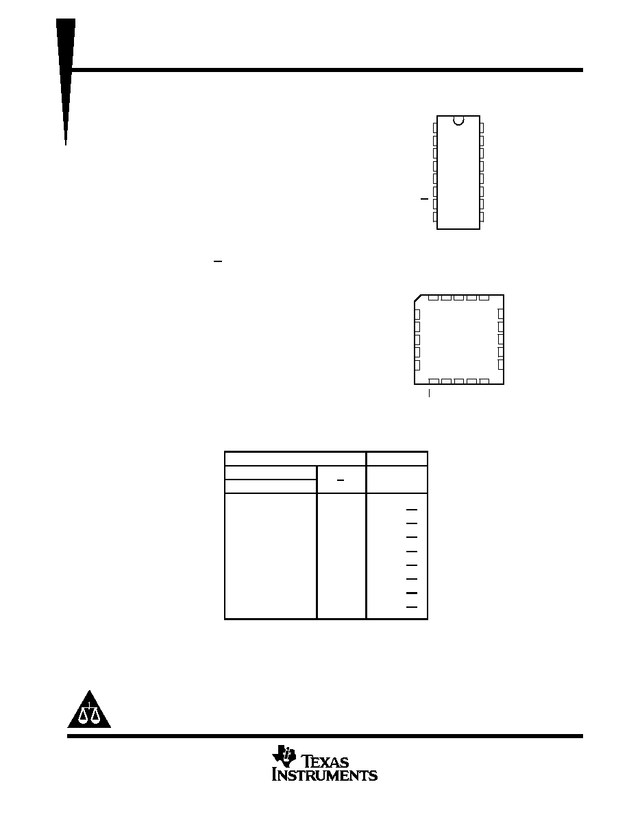
Package Options Include Plastic
Small-Outline (D) and Ceramic Flat (W)
Packages, Ceramic Chip Carriers (FK), and
Standard Plastic (N) and Ceramic (J)
300-mil DIPs
description
These monolithic data selectors/multiplexers
provide full binary decoding to select one of eight
data sources. The strobe (G) input must be at a
low logic level to enable the inputs. A high level at
the strobe terminal forces the W output high and
the Y output low.
The SN54HC151 is characterized for operation
over the full military temperature range of ≠55
∞
C
to125
∞
C. The SN74HC151 is characterized for
operation from ≠40
∞
C to 85
∞
C.
FUNCTION TABLE
INPUTS
OUTPUTS
SELECT
STROBE
Y
W
C
B
A
G
Y
W
X
X
X
H
L
H
L
L
L
L
D0
D0
L
L
H
L
D1
D1
L
H
L
L
D2
D2
L
H
H
L
D3
D3
H
L
L
L
D4
D4
H
L
H
L
D5
D5
H
H
L
L
D6
D6
H
H
H
L
D7
D7
D0, D1 . . . D7 = the level of the respective D input
1
2
3
4
5
6
7
8
16
15
14
13
12
11
10
9
D3
D2
D1
D0
Y
W
G
GND
V
CC
D4
D5
D6
D7
A
B
C
SN54HC151 . . . J OR W PACKAGE
SN74HC151 . . . D OR N PACKAGE
(TOP VIEW)
3
2 1 20 19
9 10 11 12 13
4
5
6
7
8
18
17
16
15
14
D5
D6
NC
D7
A
D1
D0
NC
Y
W
D2
D3
NC
C
B
V
D4
G
GND
NC
SN54HC151 . . . FK PACKAGE
(TOP VIEW)
CC
NC ≠ No internal connection
Copyright
©
1997, Texas Instruments Incorporated
Please be aware that an important notice concerning availability, standard warranty, and use in critical applications of
Texas Instruments semiconductor products and disclaimers thereto appears at the end of this data sheet.
PRODUCTION DATA information is current as of publication date.
Products conform to specifications per the terms of Texas Instruments
standard warranty. Production processing does not necessarily include
testing of all parameters.
SN54HC151, SN74HC151
8-LINE TO 1-LINE DATA SELECTORS/MULTIPLEXERS
SCLS110C ≠ DECEMBER 1982 ≠ MAY 1997
2
POST OFFICE BOX 655303
∑
DALLAS, TEXAS 75265
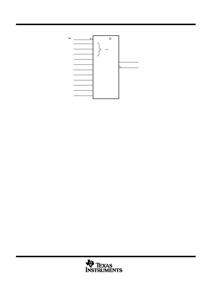
logic symbol
G 0
7
MUX
This symbol is in accordance with ANSI/IEEE Std 91-1984 and IEC Publication 617-12.
Pin numbers shown are for the D, J, N, and W packages.
W
6
Y
5
4
15
D4
5
14
D5
6
13
D6
7
12
D7
0
4
D0
1
3
D1
2
2
D2
3
1
D3
0
11
A
10
B
2
9
C
EN
7
G
SN54HC151, SN74HC151
8-LINE TO 1-LINE DATA SELECTORS/MULTIPLEXERS
SCLS110C ≠ DECEMBER 1982 ≠ MAY 1997
3
POST OFFICE BOX 655303
∑
DALLAS, TEXAS 75265
logic diagram (positive logic)
Y
5
W
6
TG
TG
TG
TG
TG
TG
TG
TG
Pin numbers shown are for the D, J, N, and W packages.
7
11
10
9
4
3
2
1
15
14
13
12
G
A
B
C
D0
D1
D2
D3
D4
D5
D6
D7
SN54HC151, SN74HC151
8-LINE TO 1-LINE DATA SELECTORS/MULTIPLEXERS
SCLS110C ≠ DECEMBER 1982 ≠ MAY 1997
4
POST OFFICE BOX 655303
∑
DALLAS, TEXAS 75265
absolute maximum ratings over operating free-air temperature range
Supply voltage range, V
CC
≠0.5 V to 7 V
. . . . . . . . . . . . . . . . . . . . . . . . . . . . . . . . . . . . . . . . . . . . . . . . . . . . . . . . . .
Input clamp current, I
IK
(V
I
< 0 or V
I
> V
CC
) (see Note 1)
±
20 mA
. . . . . . . . . . . . . . . . . . . . . . . . . . . . . . . . . . . .
Output clamp current, I
OK
(V
O
< 0 or V
O
> V
CC
) (see Note 1)
±
20 mA
. . . . . . . . . . . . . . . . . . . . . . . . . . . . . . . .
Continuous output current, I
O
(V
O
= 0 to V
CC
)
±
35 mA
. . . . . . . . . . . . . . . . . . . . . . . . . . . . . . . . . . . . . . . . . . . . . .
Continuous current through V
CC
or GND
±
70 mA
. . . . . . . . . . . . . . . . . . . . . . . . . . . . . . . . . . . . . . . . . . . . . . . . . . .
Package thermal impedance,
JA
(see Note 2): D package
113
∞
C/W
. . . . . . . . . . . . . . . . . . . . . . . . . . . . . . . . . .
N package
78
∞
C/W
. . . . . . . . . . . . . . . . . . . . . . . . . . . . . . . . . . .
Storage temperature range, T
stg
≠65
∞
C to 150
∞
C
. . . . . . . . . . . . . . . . . . . . . . . . . . . . . . . . . . . . . . . . . . . . . . . . . . .
Stresses beyond those listed under "absolute maximum ratings" may cause permanent damage to the device. These are stress ratings only, and
functional operation of the device at these or any other conditions beyond those indicated under "recommended operating conditions" is not
implied. Exposure to absolute-maximum-rated conditions for extended periods may affect device reliability.
NOTES:
1. The input and output voltage ratings may be exceeded if the input and output current ratings are observed.
2. The package thermal impedance is calculated in accordance with JESD 51, except for through-hole packages, which use a trace
length of zero.
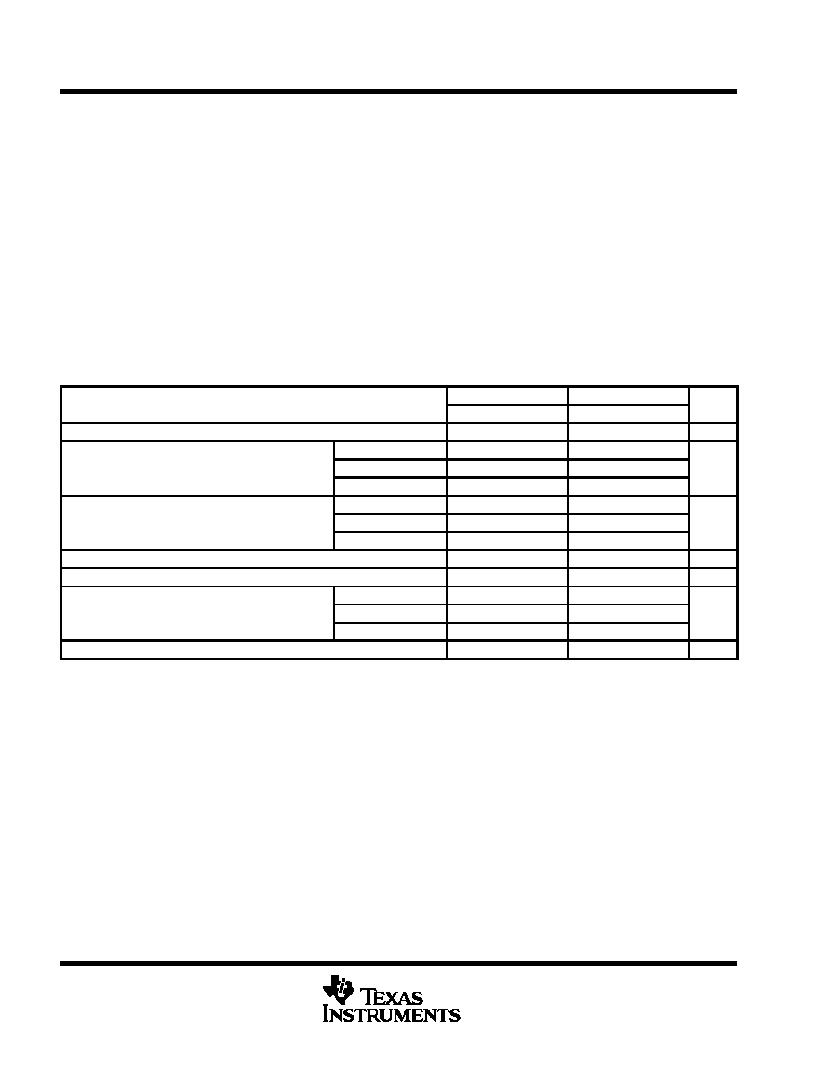
recommended operating conditions
SN54HC151
SN74HC151
UNIT
MIN
NOM
MAX
MIN
NOM
MAX
UNIT
VCC
Supply voltage
2
5
6
2
5
6
V
VCC = 2 V
1.5
1.5
VIH
High-level input voltage
VCC = 4.5 V
3.15
3.15
V
VCC = 6 V
4.2
4.2
VCC = 2 V
0
0.5
0
0.5
VIL
Low-level input voltage
VCC = 4.5 V
0
1.35
0
1.35
V
VCC = 6 V
0
1.8
0
1.8
VI
Input voltage
0
VCC
0
VCC
V
VO
Output voltage
0
VCC
0
VCC
V
VCC = 2 V
0
1000
0
1000
tt
Input transition (rise and fall) time
VCC = 4.5 V
0
500
0
500
ns
VCC = 6 V
0
400
0
400
TA
Operating free-air temperature
≠55
125
≠40
85
∞
C

SN54HC151, SN74HC151
8-LINE TO 1-LINE DATA SELECTORS/MULTIPLEXERS
SCLS110C ≠ DECEMBER 1982 ≠ MAY 1997
5
POST OFFICE BOX 655303
∑
DALLAS, TEXAS 75265
electrical characteristics over recommended operating free-air temperature range (unless
otherwise noted)
PARAMETER
TEST CONDITIONS
VCC
TA = 25
∞
C
SN54HC151
SN74HC151
UNIT
PARAMETER
TEST CONDITIONS
VCC
MIN
TYP
MAX
MIN
MAX
MIN
MAX
UNIT
2 V
1.9
1.998
1.9
1.9
IOH = ≠20
µ
A
4.5 V
4.4
4.499
4.4
4.4
VOH
VI = VIH or VIL
6 V
5.9
5.999
5.9
5.9
V
IOH = ≠6 mA
4.5 V
3.98
4.3
3.7
3.84
IOH = ≠7.8 mA
6 V
5.48
5.8
5.2
5.34
2 V
0.002
0.1
0.1
0.1
IOL = 20
µ
A
4.5 V
0.001
0.1
0.1
0.1
VOL
VI = VIH or VIL
6 V
0.001
0.1
0.1
0.1
V
IOL = 6 mA
4.5 V
0.17
0.26
0.4
0.33
IOL = 7.8 mA
6 V
0.15
0.26
0.4
0.33
II
VI = VCC or 0
6 V
±
0.1
±
100
±
1000
±
1000
nA
ICC
VI = VCC or 0,
IO = 0
6 V
8
160
80
µ
A
Ci
2 V to 6 V
3
10
10
10
pF
switching characteristics over recommended operating free-air temperature range, C
L
= 50 pF
(unless otherwise noted) (see Figure 1)
PARAMETER
FROM
TO
VCC
TA = 25
∞
C
SN54HC151
SN74HC151
UNIT
PARAMETER
(INPUT)
(OUTPUT)
VCC
MIN
TYP
MAX
MIN
MAX
MIN
MAX
UNIT
2 V
94
250
360
312
A, B, or C
Y or W
4.5 V
30
50
73
63
6 V
25
43
62
54
2 V
74
195
283
244
tpd
Any D
Y or W
4.5 V
23
39
57
49
ns
6 V
20
33
48
41
2 V
49
127
185
159
G
Y or W
4.5 V
15
25
37
32
6 V
13
22
32
28
2 V
22
75
110
95
tt
Y or W
4.5 V
9
15
22
19
ns
6 V
8
13
19
16