SN54HC164, SN74HC164
8-BIT PARALLEL-OUT SERIAL SHIFT REGISTERS
SCLS115D ≠ DECEMBER 1982 ≠ REVISED AUGUST 2003
1
POST OFFICE BOX 655303
∑
DALLAS, TEXAS 75265
D
Wide Operating Voltage Range of 2 V to 6 V
D
Outputs Can Drive Up To 10 LSTTL Loads
D
Low Power Consumption, 80-
µ
A Max I
CC
D
Typical t
pd
= 20 ns
D
±
4-mA Output Drive at 5 V
D
Low Input Current of 1
µ
A Max
D
AND-Gated (Enable / Disable) Serial Inputs
D
Fully Buffered Clock and Serial Inputs
D
Direct Clear
description/ordering information
These 8-bit shift registers feature AND-gated
serial inputs and an asynchronous clear (CLR)
input. The gated serial (A and B) inputs permit
complete control over incoming data; a low at
either input inhibits entry of the new data and
resets the first flip-flop to the low level at the next
clock (CLK) pulse. A high-level input enables the
other input, which then determines the state of the
first flip-flop. Data at the serial inputs can be
changed while CLK is high or low, provided the
minimum setup time requirements are met.
Clocking occurs on the low-to-high-level transition
of CLK.
ORDERING INFORMATION
TA
PACKAGE
ORDERABLE
PART NUMBER
TOP-SIDE
MARKING
≠40 C to 85 C
PDIP ≠ N
Tube of 25
SN74HC164N
SN74HC164N
≠40 C to 85 C
SOIC ≠ D
Tube of 50
SN74HC164D
HC164
≠40 C to 85 C
SOIC ≠ D
Reel of 2500
SN74HC164DR
HC164
≠40
∞
C to 85
∞
C
Reel of 250
SN74HC164DT
≠40
∞
C to 85
∞
C
SOP ≠ NS
Reel of 2000
SN74HC164NSR
HC164
TSSOP ≠ PW
Tube of 90
SN74HC164PW
HC164
TSSOP ≠ PW
Reel of 2000
SN74HC164PWR
HC164
Reel of 250
SN74HC164PWT
≠55 C to 125 C
CDIP ≠ J
Tube of 25
SNJ54HC164J
SNJ54HC164J
≠55
∞
C to 125
∞
C
CFP ≠ W
Tube of 150
SNJ54HC164W
SNJ54HC164W
LCCC ≠ FK
Tube of 55
SNJ54HC164FK
SNJ54HC164FK
Package drawings, standard packing quantities, thermal data, symbolization, and PCB design guidelines are
available at www.ti.com/sc/package.
Please be aware that an important notice concerning availability, standard warranty, and use in critical applications of
Texas Instruments semiconductor products and disclaimers thereto appears at the end of this data sheet.
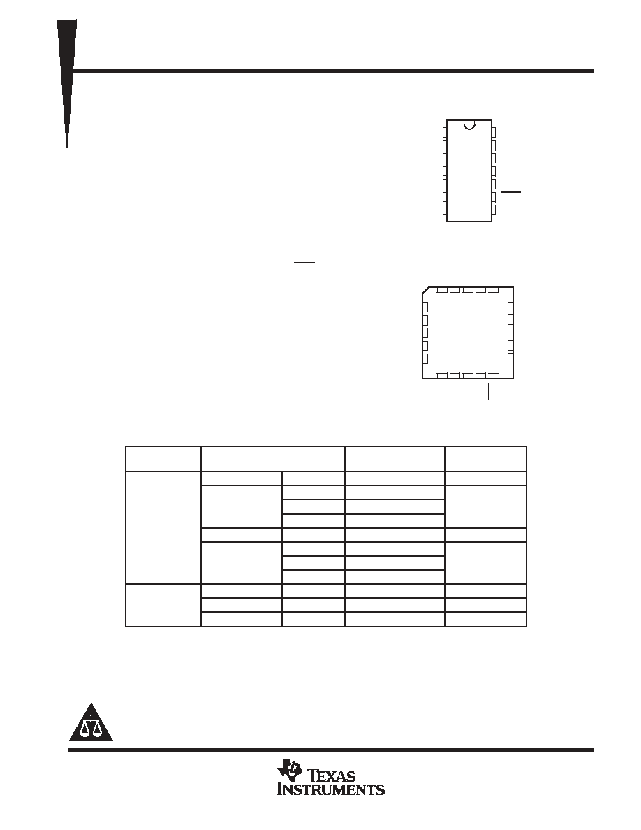
SN54HC164 . . . J OR W PACKAGE
SN74HC164 . . . D, N, NS, OR PW PACKAGE
(TOP VIEW)
1
2
3
4
5
6
7
14
13
12
11
10
9
8
A
B
Q
A
Q
B
Q
C
Q
D
GND
V
CC
Q
H
Q
G
Q
F
Q
E
CLR
CLK
3
2 1 20 19
9 10 11 12 13
4
5
6
7
8
18
17
16
15
14
Q
G
NC
Q
F
NC
Q
E
Q
A
NC
Q
B
NC
Q
C
B
A
NC
CLK
CLR
V
Q
D
GND
NC
SN54HC164 . . . FK PACKAGE
(TOP VIEW)
CC
H
Q
NC ≠ No internal connection
Copyright
2003, Texas Instruments Incorporated
PRODUCTION DATA information is current as of publication date.
Products conform to specifications per the terms of Texas Instruments
standard warranty. Production processing does not necessarily include
testing of all parameters.
On products compliant to MIL-PRF-38535, all parameters are tested
unless otherwise noted. On all other products, production
processing does not necessarily include testing of all parameters.
SN54HC164, SN74HC164
8-BIT PARALLEL-OUT SERIAL SHIFT REGISTERS
SCLS115D ≠ DECEMBER 1982 ≠ REVISED AUGUST 2003
2
POST OFFICE BOX 655303
∑
DALLAS, TEXAS 75265
FUNCTION TABLE
INPUTS
OUTPUTS
CLR
CLK
A
B
QA
QB . . . QH
L
X
X
X
L
L
L
H
L
X
X
QA0
QB0
QH0
H
H
H
H
QAn
QGn
H
L
X
L
QAn
QGn
H
X
L
L
QAn
QGn
QA0, QB0, QH0 = the level of QA, QB, or QH, respectively,
before the indicated steady-state input conditions were
established
QAn, QGn = the level of QA or QG before the most recent
transition of CLK: indicates a 1-bit shift
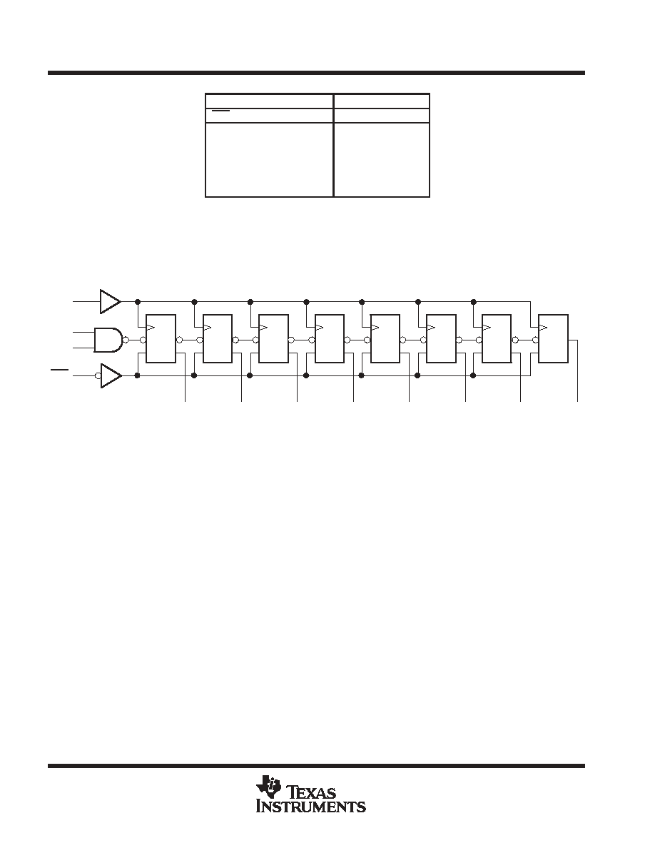
logic diagram (positive logic)
9
A
B
CLR
CLK
Pin numbers shown are for the D, J, N, NS, PW, and W packages.
C1
1D
R
3
QA
C1
1D
R
4
QB
C1
1D
R
5
QC
C1
1D
R
6
QD
C1
1D
R
10
QE
C1
1D
R
11
QF
C1
1D
R
12
QG
C1
1D
R
13
QH
2
1
8
SN54HC164, SN74HC164
8-BIT PARALLEL-OUT SERIAL SHIFT REGISTERS
SCLS115D ≠ DECEMBER 1982 ≠ REVISED AUGUST 2003
3
POST OFFICE BOX 655303
∑
DALLAS, TEXAS 75265
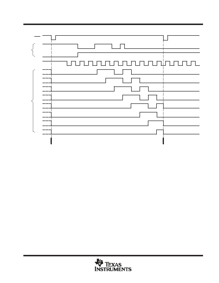
typical clear, shift, and clear sequence
CLK
A
B
CLR
QA
QB
QC
QD
QE
QF
QG
QH
Clear
Clear
Serial Inputs
Outputs
absolute maximum ratings over operating free-air temperature range (unless otherwise noted)
Supply voltage range, V
CC
≠0.5 V to 7 V
. . . . . . . . . . . . . . . . . . . . . . . . . . . . . . . . . . . . . . . . . . . . . . . . . . . . . . . . . .
Input clamp current, I
IK
(V
I
< 0 or V
I
> V
CC
) (see Note 1)
±
20 mA
. . . . . . . . . . . . . . . . . . . . . . . . . . . . . . . . . . . .
Output clamp current, I
OK
(V
O
< 0 or V
O
> V
CC
) (see Note 1)
±
20 mA
. . . . . . . . . . . . . . . . . . . . . . . . . . . . . . . .
Continuous output current, I
O
(V
O
= 0 to V
CC
)
±
25 mA
. . . . . . . . . . . . . . . . . . . . . . . . . . . . . . . . . . . . . . . . . . . . . .
Continuous current through V
CC
or GND
±
50 mA
. . . . . . . . . . . . . . . . . . . . . . . . . . . . . . . . . . . . . . . . . . . . . . . . . . .
Package thermal impedance,
JA
(see Note 2): D package
86
∞
C/W
. . . . . . . . . . . . . . . . . . . . . . . . . . . . . . . . . . .
N package
80
∞
C/W
. . . . . . . . . . . . . . . . . . . . . . . . . . . . . . . . . . .
NS package
76
∞
C/W
. . . . . . . . . . . . . . . . . . . . . . . . . . . . . . . . .
PW package
113
∞
C/W
. . . . . . . . . . . . . . . . . . . . . . . . . . . . . . . .
Storage temperature range, T
stg
≠65
∞
C to 150
∞
C
. . . . . . . . . . . . . . . . . . . . . . . . . . . . . . . . . . . . . . . . . . . . . . . . . . .
Stresses beyond those listed under "absolute maximum ratings" may cause permanent damage to the device. These are stress ratings only, and
functional operation of the device at these or any other conditions beyond those indicated under "recommended operating conditions" is not
implied. Exposure to absolute-maximum-rated conditions for extended periods may affect device reliability.
NOTES:
1. The input and output voltage ratings may be exceeded if the input and output current ratings are observed.
2. The package thermal impedance is calculated in accordance with JESD 51-7.
SN54HC164, SN74HC164
8-BIT PARALLEL-OUT SERIAL SHIFT REGISTERS
SCLS115D ≠ DECEMBER 1982 ≠ REVISED AUGUST 2003
4
POST OFFICE BOX 655303
∑
DALLAS, TEXAS 75265
recommended operating conditions (see Note 3)
SN54HC164
SN74HC164
UNIT
MIN
NOM
MAX
MIN
NOM
MAX
UNIT
VCC
Supply voltage
2
5
6
2
5
6
V
V
High-level input voltage
VCC = 2 V
1.5
1.5
V
VIH
High-level input voltage
VCC = 4.5 V
3.15
3.15
V
IH
VCC = 6 V
4.2
4.2
V
Low-level input voltage
VCC = 2 V
0.5
0.5
V
VIL
Low-level input voltage
VCC = 4.5 V
1.35
1.35
V
IL
VCC = 6 V
1.8
1.8
VI
Input voltage
0
VCC
0
VCC
V
VO
Output voltage
0
VCC
0
VCC
V
t/ v
Input transition rise/fall time
VCC = 2 V
1000
1000
ns
t/
v
Input transition rise/fall time
VCC = 4.5 V
500
500
ns
VCC = 6 V
400
400
TA
Operating free-air temperature
≠55
125
≠40
85
∞
C
NOTE 3: All unused inputs of the device must be held at VCC or GND to ensure proper device operation. Refer to the TI application report,
Implications of Slow or Floating CMOS Inputs, literature number SCBA004.
If this device is used in the threshold region (from VILmax = 0.5 V to VIHmin = 1.5 V), there is a potential to go into the wrong state from induced
grounding, causing double clocking. Operating with the inputs at tt = 1000 ns and VCC = 2 V does not damage the device; however, functionally,
the CLK inputs are not ensured while in the shift, count, or toggle operating modes.
electrical characteristics over recommended operating free-air temperature range (unless
otherwise noted)
PARAMETER
TEST CONDITIONS
VCC
TA = 25
∞
C
SN54HC164
SN74HC164
UNIT
PARAMETER
TEST CONDITIONS
VCC
MIN
TYP
MAX
MIN
MAX
MIN
MAX
UNIT
V
V = V
or V
I
= ≠20 A
2 V
1.9
1.998
1.9
1.9
V
V
V = V
or V
IOH = ≠20
µ
A
4.5 V
4.4
4.499
4.4
4.4
V
VOH
VI = VIH or VIL
OH
6 V
5.9
5.999
5.9
5.9
V
OH
I
IH
IL
IOH = ≠4 mA
4.5 V
3.98
4.3
3.7
3.84
IOH = ≠5.2 mA
6 V
5.48
5.8
5.2
5.34
V
V = V
or V
I
= 20 A
2 V
0.002
0.1
0.1
0.1
V
V
V = V
or V
IOL = 20
µ
A
4.5 V
0.001
0.1
0.1
0.1
V
VOL
VI = VIH or VIL
OL
6 V
0.001
0.1
0.1
0.1
V
OL
I
IH
IL
IOL = 4 mA
4.5 V
0.17
0.26
0.4
0.33
IOL = 5.2 mA
6 V
0.15
0.26
0.4
0.33
II
VI = VCC or 0
6 V
±
0.1
±
100
±
1000
±
1000
nA
ICC
VI = VCC or 0,
IO = 0
6 V
8
160
80
µ
A
Ci
2 V to 6 V
3
10
10
10
pF
SN54HC164, SN74HC164
8-BIT PARALLEL-OUT SERIAL SHIFT REGISTERS
SCLS115D ≠ DECEMBER 1982 ≠ REVISED AUGUST 2003
5
POST OFFICE BOX 655303
∑
DALLAS, TEXAS 75265
timing requirements over recommended operating free-air temperature range (unless otherwise
noted)
VCC
TA = 25
∞
C
SN54HC164
SN74HC164
UNIT
VCC
MIN
MAX
MIN
MAX
MIN
MAX
UNIT
f
Clock frequency
2 V
6
4.2
5
MHz
fclock
Clock frequency
4.5 V
31
21
25
MHz
clock
6 V
36
25
28
t
Pulse duration
CLR low
2 V
100
150
125
ns
t
Pulse duration
CLR low
4.5 V
20
30
25
ns
tw
Pulse duration
6 V
17
25
21
ns
tw
Pulse duration
CLK high or low
2 V
80
120
100
ns
CLK high or low
4.5 V
16
24
20
6 V
14
20
18
t
Setup time before CLK
Data
2 V
100
150
125
ns
t
Setup time before CLK
Data
4.5 V
20
30
25
ns
tsu
Setup time before CLK
6 V
17
25
21
ns
tsu
Setup time before CLK
CLR inactive
2 V
100
150
125
ns
CLR inactive
4.5 V
20
30
25
6 V
17
25
21
t
Hold time, data after CLK
2 V
5
5
5
ns
th
Hold time, data after CLK
4.5 V
5
5
5
ns
h
6 V
5
5
5
switching characteristics over recommended operating free-air temperature range, C
L
= 50 pF
(unless otherwise noted) (see Figure 1)
PARAMETER
FROM
TO
VCC
TA = 25
∞
C
SN54HC164
SN74HC164
UNIT
PARAMETER
FROM
(INPUT)
TO
(OUTPUT)
VCC
MIN
TYP
MAX
MIN
MAX
MIN
MAX
UNIT
f
2 V
6
10
4.2
5
MHz
fmax
4.5 V
31
54
21
25
MHz
max
6 V
36
62
25
28
t
CLR
Any Q
2 V
140
205
295
255
ns
tPHL
CLR
Any Q
4.5 V
28
41
59
51
ns
PHL
6 V
24
35
51
46
ns
t
CLK
Any Q
2 V
115
175
265
220
ns
tpd
CLK
Any Q
4.5 V
23
35
53
44
pd
6 V
20
30
45
38
t
2 V
38
75
110
95
ns
tt
4.5 V
8
15
22
19
ns
t
6 V
6
13
19
16
operating characteristics, T
A
= 25
∞
C
PARAMETER
TEST CONDITIONS
TYP
UNIT
Cpd
Power dissipation capacitance
No load
135
pF