SN54HC166, SN74HC166
8-BIT PARALLEL-LOAD SHIFT REGISTERS
SCLS117B ≠ DECEMBER 1982 ≠ REVISED MAY 1997
1
POST OFFICE BOX 655303
∑
DALLAS, TEXAS 75265
D
Synchronous Load
D
Direct Overriding Clear
D
Parallel-to-Serial Conversion
D
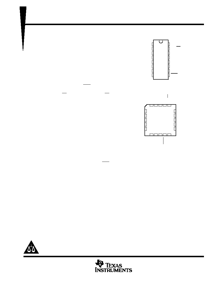
Package Options Include Plastic
Small-Outline (D) and Ceramic Flat (W)
Packages, Ceramic Chip Carriers (FK), and
Standard Plastic (N) and Ceramic (J)
300-mil DIPs
description
The 'HC166 parallel-in or serial-in, serial-out
registers feature gated clock (CLK, CLK INH)
inputs and an overriding clear (CLR) input. The
parallel-in or serial-in modes are established by
the shift / load (SH/LD) input. When high, SH/LD
enables the serial (SER) data input and couples
the eight flip-flops for serial shifting with each
clock (CLK) pulse. When low, the parallel
(broadside) data inputs are enabled, and
synchronous loading occurs on the next clock
pulse. During parallel loading, serial data flow is
inhibited. Clocking is accomplished on the
low-to-high-level edge of CLK through a 2-input
positive-NOR gate permitting one input to be used
as a clock-enable or clock-inhibit function. Holding
either CLK or CLK INH high inhibits clocking;
holding either low enables the other clock input.
This allows the system clock to be free running,
and the register can be stopped on command with
the other clock input. CLK INH should be changed
to the high level only when CLK is high. CLR
overrides all other inputs, including CLK, and
resets all flip-flops to zero.
The SN54HC166 is characterized for operation over the full military temperature range of ≠55
∞
C to 125
∞
C. The
SN74HC166 is characterized for operation from ≠40
∞
C to 85
∞
C.
Please be aware that an important notice concerning availability, standard warranty, and use in critical applications of
Texas Instruments semiconductor products and disclaimers thereto appears at the end of this data sheet.
3
2 1 20 19
9 10 11 12 13
4
5
6
7
8
18
17
16
15
14
H
Q
H
NC
G
F
B
C
NC
D
CLK INH
A
SER
NC
CLR
E
V
SH/LD
CLK
GND
NC
SN54HC166 . . . FK PACKAGE
(TOP VIEW)
CC
NC ≠ No internal connection
1
2
3
4
5
6
7
8
16
15
14
13
12
11
10
9
SER
A
B
C
D
CLK INH
CLK
GND
V
CC
SH/LD
H
Q
H
G
F
E
CLR
SN54HC166 . . . J OR W PACKAGE
SN74HC166 . . . D OR N PACKAGE
(TOP VIEW)
Copyright
©
1997, Texas Instruments Incorporated
PRODUCTION DATA information is current as of publication date.
Products conform to specifications per the terms of Texas Instruments
standard warranty. Production processing does not necessarily include
testing of all parameters.

SN54HC166, SN74HC166
8-BIT PARALLEL-LOAD SHIFT REGISTERS
SCLS117B ≠ DECEMBER 1982 ≠ REVISED MAY 1997
2
POST OFFICE BOX 655303
∑
DALLAS, TEXAS 75265
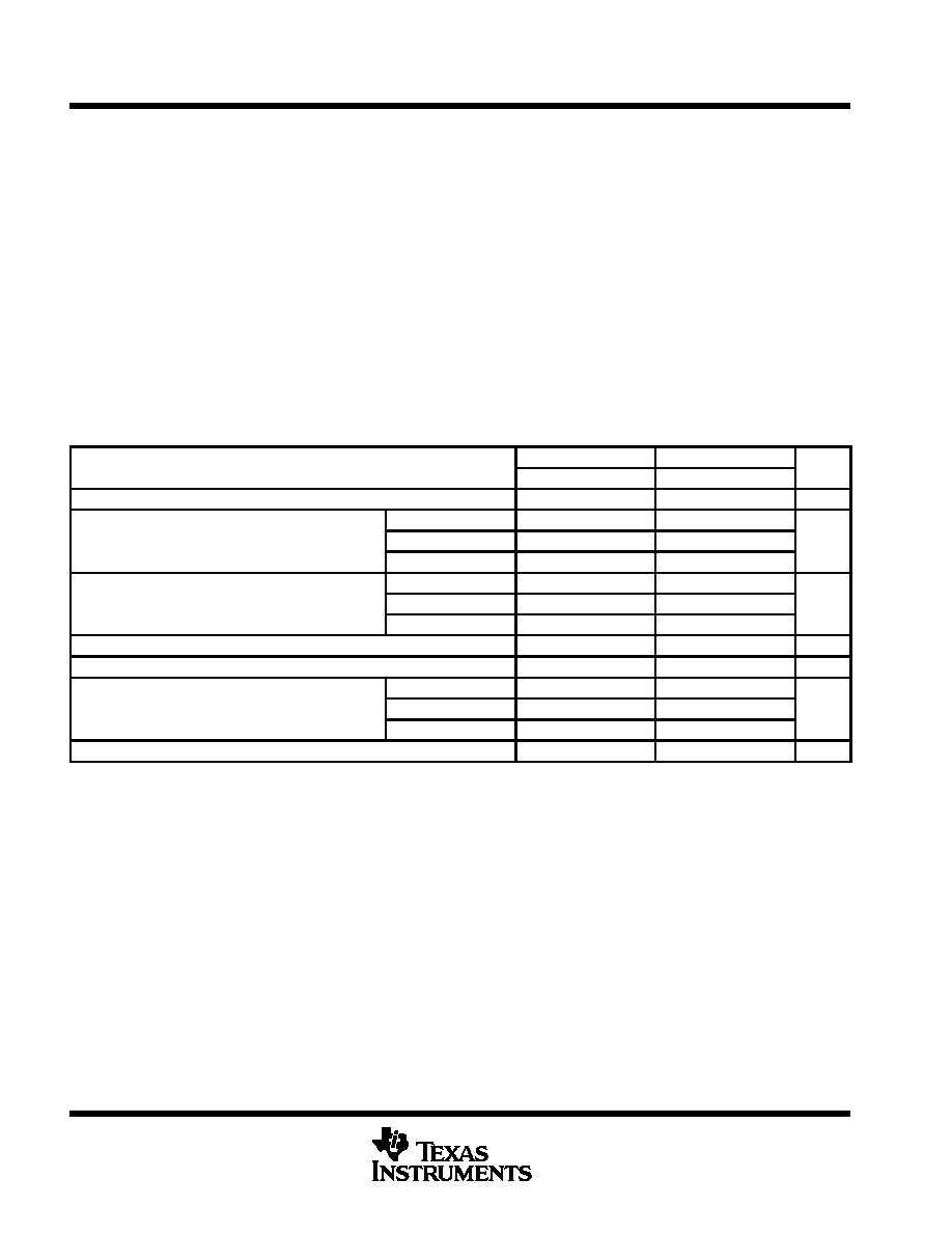
FUNCTION TABLE
INPUTS
OUTPUTS
INPUTS
INTERNAL
CLR
SH/LD
CLK INH
CLK
SER
PARALLEL
A . . . H
QA
QB
QH
L
X
X
X
X
X
L
L
L
H
X
L
L
X
X
QA0
QB0
QH0
H
L
L
X
a . . . h
a
b
h
H
H
L
H
X
H
QAn
QGn
H
H
L
L
X
L
QAn
QGn
H
X
H
X
X
QA0
QB0
QH0
logic symbol
CLR
SRG8
R
9
M1 [Shift]
15
M2 [Load]
6
CLK INH
7
CLK
C3/1
2, 3D
3
B
4
C
5
D
10
E
11
F
12
G
14
H
1, 3D
1
SER
2, 3D
2
A
13
1
QH
SH/LD
This symbol is in accordance with ANSI/IEEE Std 91-1984 and IEC Publication 617-12.
Pin numbers shown are for the D, J, N, and W packages.

SN54HC166, SN74HC166
8-BIT PARALLEL-LOAD SHIFT REGISTERS
SCLS117B ≠ DECEMBER 1982 ≠ REVISED MAY 1997
3
POST OFFICE BOX 655303
∑
DALLAS, TEXAS 75265
logic diagram (positive logic)
1D
C1
15
9
7
6
13
SH/LD
CLR
CLK
CLK INH
QH
2
3
4
5
10
11
12
14
SER
A
B
C
D
E
F
G
H
R
1D
C1
R
1D
C1
R
1D
C1
R
1D
C1
R
1D
C1
R
1D
C1
R
1D
C1
R
1
Pin numbers shown are for the D, J, N, and W packages.
typical clear, shift, load, inhibit, and shift sequence
Clear
Load
Inhibit
H
H
H
H
H
H
H
H
H
H
L
L
L
L
L
L
CLK
CLK INH
SER
A
B
C
D
E
F
G
H
SH/LD
CLR
QH
Parallel
Inputs
Serial Shift
Serial Shift
SN54HC166, SN74HC166
8-BIT PARALLEL-LOAD SHIFT REGISTERS
SCLS117B ≠ DECEMBER 1982 ≠ REVISED MAY 1997
4
POST OFFICE BOX 655303
∑
DALLAS, TEXAS 75265
absolute maximum ratings over operating free-air temperature range
Supply voltage range, V
CC
≠0.5 V to 7 V
. . . . . . . . . . . . . . . . . . . . . . . . . . . . . . . . . . . . . . . . . . . . . . . . . . . . . . . . . .
Input clamp current, I
IK
(V
I
< 0 or V
I
> V
CC
) (see Note 1)
±
20 mA
. . . . . . . . . . . . . . . . . . . . . . . . . . . . . . . . . . . .
Output clamp current, I
OK
(V
O
< 0 or V
O
> V
CC
) (see Note 1)
±
20 mA
. . . . . . . . . . . . . . . . . . . . . . . . . . . . . . . .
Continuous output current, I
O
(V
O
= 0 to V
CC
)
±
25 mA
. . . . . . . . . . . . . . . . . . . . . . . . . . . . . . . . . . . . . . . . . . . . . .
Continuous current through V
CC
or GND
±
50 mA
. . . . . . . . . . . . . . . . . . . . . . . . . . . . . . . . . . . . . . . . . . . . . . . . . . .
Package thermal impedance,
JA
(see Note 2): D package
113
∞
C/W
. . . . . . . . . . . . . . . . . . . . . . . . . . . . . . . . . .
N package
78
∞
C/W
. . . . . . . . . . . . . . . . . . . . . . . . . . . . . . . . . . .
Storage temperature range, T
stg
≠65
∞
C to 150
∞
C
. . . . . . . . . . . . . . . . . . . . . . . . . . . . . . . . . . . . . . . . . . . . . . . . . . .
Stresses beyond those listed under "absolute maximum ratings" may cause permanent damage to the device. These are stress ratings only, and
functional operation of the device at these or any other conditions beyond those indicated under "recommended operating conditions" is not
implied. Exposure to absolute-maximum-rated conditions for extended periods may affect device reliability.
NOTES:
1. The input and output voltage ratings may be exceeded if the input and output current ratings are observed.
2. The package thermal impedance is calculated in accordance with JESD 51, except for through-hole packages, which use a trace
length of zero.
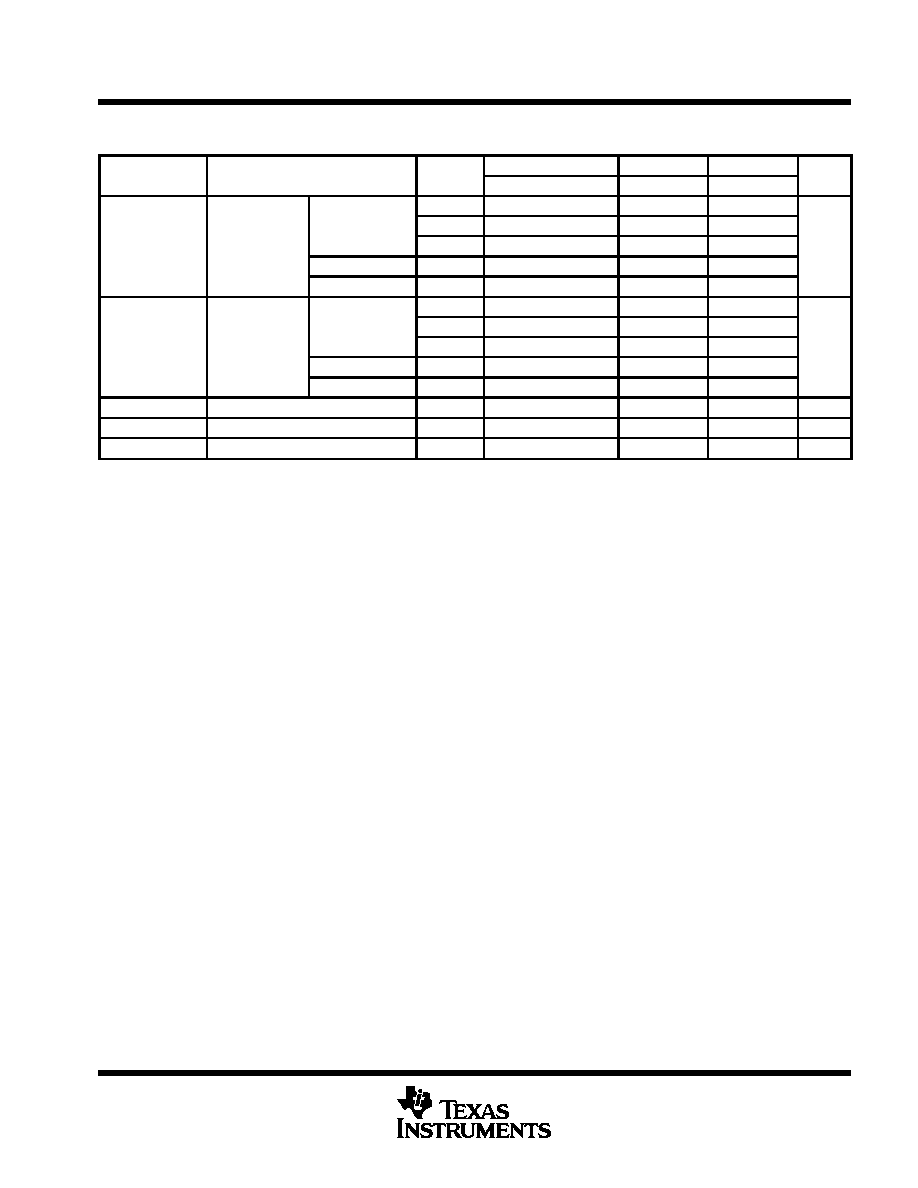
recommended operating conditions
SN54HC166
SN74HC166
UNIT
MIN
NOM
MAX
MIN
NOM
MAX
UNIT
VCC
Supply voltage
2
5
6
2
5
6
V
VCC = 2 V
1.5
1.5
VIH
High-level input voltage
VCC = 4.5 V
3.15
3.15
V
VCC = 6 V
4.2
4.2
VCC = 2 V
0
0.5
0
0.5
VIL
Low-level input voltage
VCC = 4.5 V
0
1.35
0
1.35
V
VCC = 6 V
0
1.8
0
1.8
VI
Input voltage
0
VCC
0
VCC
V
VO
Output voltage
0
VCC
0
VCC
V
VCC = 2 V
0
1000
0
1000
tt
Input transition (rise and fall) time
VCC = 4.5 V
0
500
0
500
ns
VCC = 6 V
0
400
0
400
TA
Operating free-air temperature
≠55
125
≠40
85
∞
C
If this device is used in the threshold region (from VILmax = 0.5 V to VIHmin = 1.5 V), there is a potential to go into the wrong state from induced
grounding, causing double clocking. Operating with the inputs at tt = 1000 ns and VCC = 2 V does not damage the device; however, functionally,
the CLK inputs are not ensured while in the shift, count, or toggle operating modes.
SN54HC166, SN74HC166
8-BIT PARALLEL-LOAD SHIFT REGISTERS
SCLS117B ≠ DECEMBER 1982 ≠ REVISED MAY 1997
5
POST OFFICE BOX 655303
∑
DALLAS, TEXAS 75265
electrical characteristics over recommended operating free-air temperature range (unless
otherwise noted)
PARAMETER
TEST CONDITIONS
VCC
TA = 25
∞
C
SN54HC166
SN74HC166
UNIT
PARAMETER
TEST CONDITIONS
VCC
MIN
TYP
MAX
MIN
MAX
MIN
MAX
UNIT
2 V
1.9
1.998
1.9
1.9
IOH = ≠20
µ
A
4.5 V
4.4
4.499
4.4
4.4
VOH
VI = VIH or VIL
6 V
5.9
5.999
5.9
5.9
V
IOH = ≠4 mA
4.5 V
3.98
4.3
3.7
3.84
IOH = ≠5.2 mA
6 V
5.48
5.8
5.2
5.34
2 V
0.002
0.1
0.1
0.1
IOL = 20
µ
A
4.5 V
0.001
0.1
0.1
0.1
VOL
VI = VIH or VIL
6 V
0.001
0.1
0.1
0.1
V
IOL = 4 mA
4.5 V
0.17
0.26
0.4
0.33
IOL = 5.2 mA
6 V
0.15
0.26
0.4
0.33
II
VI = VCC or 0
6 V
±
0.1
±
100
±
1000
±
1000
nA
ICC
VI = VCC or 0,
IO = 0
6 V
8
160
80
µ
A
Ci
2 V to 6 V
3
10
10
10
pF