SN54LV139A, SN74LV139A
DUAL 2-LINE TO 4-LINE DECODERS/DEMULTIPLEXERS
SCLS396G ≠ APRIL 1998 ≠ REVISED JULY 2003
1
POST OFFICE BOX 655303
∑
DALLAS, TEXAS 75265
D
2-V to 5.5-V V
CC
Operation
D
Max t
pd
of 7.5 ns at 5 V
D
Support Mixed-Mode Voltage Operation on
All Ports
D
Designed Specifically for High-Speed
Memory Decoders and Data-Transmission
Systems
D
Incorporate Two Enable Inputs to Simplify
Cascading and/or Data Reception
D
I
off
Supports Partial-Power-Down Mode
Operation
D
Latch-Up Performance Exceeds 250 mA Per
JESD 17
D
ESD Protection Exceeds JESD 22
≠ 2000-V Human-Body Model (A114-A)
≠ 200-V Machine Model (A115-A)
≠ 1000-V Charged-Device Model (C101)
3
2 1 20 19
9 10 11 12 13
4
5
6
7
8
18
17
16
15
14
2A
2B
NC
2Y0
2Y1
1B
1Y0
NC
1Y1
1Y2
1A
1G
NC
2Y3
2Y2
V
2G
1Y3
GND
NC
SN54LV139A . . . FK PACKAGE
(TOP VIEW)
CC
NC ≠ No internal connection
1
2
3
4
5
6
7
8
16
15
14
13
12
11
10
9
1G
1A
1B
1Y0
1Y1
1Y2
1Y3
GND
V
CC
2G
2A
2B
2Y0
2Y1
2Y2
2Y3
SN54LV139A . . . J OR W PACKAGE
SN74LV139A . . . D, DB, DGV, NS,
OR PW PACKAGE
(TOP VIEW)
SN74LV139A . . . RGY PACKAGE
(TOP VIEW)
1
16
8
9
2
3
4
5
6
7
15
14
13
12
11
10
2G
2A
2B
2Y0
2Y1
2Y2
1A
1B
1Y0
1Y1
1Y2
1Y3
1G
2Y3
V
GND
CC
description/ordering information
The 'LV139A devices are dual 2-line to 4-line decoders/demultiplexers designed for 2-V to 5.5-V V
CC
operation.
ORDERING INFORMATION
TA
PACKAGE
ORDERABLE
PART NUMBER
TOP-SIDE
MARKING
QFN ≠ RGY
Reel of 1000
SN74LV139ARGYR
LV139A
SOIC
D
Tube of 40
SN74LV139AD
LV139A
SOIC ≠ D
Reel of 2500
SN74LV139ADR
LV139A
SOP ≠ NS
Reel of 2000
SN74LV139ANSR
74LV139A
≠40
∞
C to 85
∞
C
SSOP ≠ DB
Reel of 2000
SN74LV139ADBR
LV139A
Tube of 90
SN74LV139APW
TSSOP ≠ PW
Reel of 2000
SN74LV139APWR
LV139A
Reel of 250
SN74LV139APWT
TVSOP ≠ DGV
Reel of 2000
SN74LV139ADGVR
LV139A
CDIP ≠ J
Tube of 25
SNJ54LV139AJ
SNJ54LV139AJ
≠55
∞
C to 125
∞
C
CFP ≠ W
Tube of 150
SNJ54LV139AW
SNJ54LV139AW
LCCC ≠ FK
Tube of 55
SNJ54LV139AFK
SNJ54LV139AFK
Package drawings, standard packing quantities, thermal data, symbolization, and PCB design
guidelines are available at www.ti.com/sc/package.
UNLESS OTHERWISE NOTED this document contains PRODUCTION
DATA information current as of publication date. Products conform to
specifications per the terms of Texas Instruments standard warranty.
Production processing does not necessarily include testing of all
parameters.
Copyright
2003, Texas Instruments Incorporated
Please be aware that an important notice concerning availability, standard warranty, and use in critical applications of
Texas Instruments semiconductor products and disclaimers thereto appears at the end of this data sheet.
SN54LV139A, SN74LV139A
DUAL 2-LINE TO 4-LINE DECODERS/DEMULTIPLEXERS
SCLS396G ≠ APRIL 1998 ≠ REVISED JULY 2003
2
POST OFFICE BOX 655303
∑
DALLAS, TEXAS 75265
description/ordering information(continued)
These devices are designed for high-performance memory-decoding or data-routing applications requiring very
short propagation delay times. In high-performance memory systems, these decoders can minimize the effects
of system decoding. When employed with high-speed memories utilizing a fast enable circuit, the delay time
of these decoders and the enable time of the memory usually are less than the typical access time of the
memory. This means that the effective system delay introduced by the decoders is negligible.
The 'LV139A devices comprise two individual 2-line to 4-line decoders in a single package. The active-low
enable (G) input can be used as a data line in demultiplexing applications. These decoders/demultiplexers
feature fully buffered inputs, each of which represents only one normalized load to its driving circuit.
These devices are fully specified for partial-power-down applications using I
off
. The I
off
circuitry disables the
outputs, preventing damaging current backflow through the devices when they are powered down.
FUNCTION TABLE
INPUTS
OUTPUTS
G
SELECT
OUTPUTS
G
B
A
Y0
Y1
Y2
Y3
H
X
X
H
H
H
H
L
L
L
L
H
H
H
L
L
H
H
L
H
H
L
H
L
H
H
L
H
L
H
H
H
H
H
L
SN54LV139A, SN74LV139A
DUAL 2-LINE TO 4-LINE DECODERS/DEMULTIPLEXERS
SCLS396G ≠ APRIL 1998 ≠ REVISED JULY 2003
3
POST OFFICE BOX 655303
∑
DALLAS, TEXAS 75265
logic diagram (positive logic)
1G
1Y0
1Y1
1Y2
1Y3
2Y0
2Y1
2Y2
2Y3
1A
1B
2G
2A
2B
Pin numbers shown are for the D, DB, DGV, J, NS, PW, RGY, and W packages.
1
2
3
15
14
13
4
5
6
7
12
11
10
9
absolute maximum ratings over operating free-air temperature range (unless otherwise noted)
Supply voltage range, V
CC
≠0.5 V to 7 V
. . . . . . . . . . . . . . . . . . . . . . . . . . . . . . . . . . . . . . . . . . . . . . . . . . . . . . . . . .
Input voltage range, V
I
(see Note 1)
≠0.5 V to 7 V
. . . . . . . . . . . . . . . . . . . . . . . . . . . . . . . . . . . . . . . . . . . . . . . . . .
Voltage range applied to any output in the high-impedance
or power-off state, V
O
(see Note 1)
≠0.5 V to 7 V
. . . . . . . . . . . . . . . . . . . . . . . . . . . . . . . . . . . . . . . . . . . . . . . .
Output voltage range, V
O
(see Notes 1 and 2)
≠0.5 V to V
CC
+ 0.5 V
. . . . . . . . . . . . . . . . . . . . . . . . . . . . . . . . . .
Input clamp current, I
IK
(V
I
< 0)
≠20 mA
. . . . . . . . . . . . . . . . . . . . . . . . . . . . . . . . . . . . . . . . . . . . . . . . . . . . . . . . . . .
Output clamp current, I
OK
(V
O
< 0 or V
O
> V
CC
)
±
50 mA
. . . . . . . . . . . . . . . . . . . . . . . . . . . . . . . . . . . . . . . . . . . .
Continuous output current, I
O
(V
O
= 0 to V
CC
)
±
25 mA
. . . . . . . . . . . . . . . . . . . . . . . . . . . . . . . . . . . . . . . . . . . . . .
Continuous current through V
CC
or GND
±
50 mA
. . . . . . . . . . . . . . . . . . . . . . . . . . . . . . . . . . . . . . . . . . . . . . . . . . .
Package thermal impedance,
JA
(see Note 3): D package
73
∞
C/W
. . . . . . . . . . . . . . . . . . . . . . . . . . . . . . . . . . .
(see Note 3): DB package
82
∞
C/W
. . . . . . . . . . . . . . . . . . . . . . . . . . . . . . . . .
(see Note 3): DGV package
120
∞
C/W
. . . . . . . . . . . . . . . . . . . . . . . . . . . . . . .
(see Note 3): NS package
64
∞
C/W
. . . . . . . . . . . . . . . . . . . . . . . . . . . . . . . . .
(see Note 3): PW package
108
∞
C/W
. . . . . . . . . . . . . . . . . . . . . . . . . . . . . . . .
(see Note 4): RGY package
39
∞
C/W
. . . . . . . . . . . . . . . . . . . . . . . . . . . . . . . .
Storage temperature range, T
stg
≠65
∞
C to 150
∞
C
. . . . . . . . . . . . . . . . . . . . . . . . . . . . . . . . . . . . . . . . . . . . . . . . . . .
Stresses beyond those listed under "absolute maximum ratings" may cause permanent damage to the device. These are stress ratings only, and
functional operation of the device at these or any other conditions beyond those indicated under "recommended operating conditions" is not
implied. Exposure to absolute-maximum-rated conditions for extended periods may affect device reliability.
NOTES:
1. The input and output voltage ratings may be exceeded if the input and output current ratings are observed.
2. This value is limited to 5.5 V maximum.
3. The package thermal impedance is calculated in accordance with JESD 51-7.
4. The package thermal impedance is calculated in accordance with JESD 51-5.
SN54LV139A, SN74LV139A
DUAL 2-LINE TO 4-LINE DECODERS/DEMULTIPLEXERS
SCLS396G ≠ APRIL 1998 ≠ REVISED JULY 2003
4
POST OFFICE BOX 655303
∑
DALLAS, TEXAS 75265
recommended operating conditions (see Note 5)
SN54LV139A
SN74LV139A
UNIT
MIN
MAX
MIN
MAX
UNIT
VCC
Supply voltage
2
5.5
2
5.5
V
VCC = 2 V
1.5
1.5
VIH
High level input voltage
VCC = 2.3 V to 2.7 V
VCC
◊
0.7
VCC
◊
0.7
V
VIH
High-level input voltage
VCC = 3 V to 3.6 V
VCC
◊
0.7
VCC
◊
0.7
V
VCC = 4.5 V to 5.5 V
VCC
◊
0.7
VCC
◊
0.7
VCC = 2 V
0.5
0.5
VIL
Low level input voltage
VCC = 2.3 V to 2.7 V
VCC
◊
0.3
VCC
◊
0.3
V
VIL
Low-level input voltage
VCC = 3 V to 3.6 V
VCC
◊
0.3
VCC
◊
0.3
V
VCC = 4.5 V to 5.5 V
VCC
◊
0.3
VCC
◊
0.3
VI
Input voltage
0
5.5
0
5.5
V
VO
Output voltage
0
VCC
0
VCC
V
VCC = 2 V
≠50
≠50
µ
A
IOH
High level output current
VCC = 2.3 V to 2.7 V
≠2
≠2
IOH
High-level output current
VCC = 3 V to 3.6 V
≠6
≠6
mA
VCC = 4.5 V to 5.5 V
≠12
≠12
VCC = 2 V
50
50
µ
A
IOL
Low level output current
VCC = 2.3 V to 2.7 V
2
2
IOL
Low-level output current
VCC = 3 V to 3.6 V
6
6
mA
VCC = 4.5 V to 5.5 V
12
12
VCC = 2.3 V to 2.7 V
200
200
t/
v
Input transition rise or fall rate
VCC = 3 V to 3.6 V
100
100
ns/V
VCC = 4.5 V to 5.5 V
20
20
TA
Operating free-air temperature
≠55
125
≠40
85
∞
C
NOTE 5: All unused inputs of the device must be held at VCC or GND to ensure proper device operation. Refer to the TI application report,
Implications of Slow or Floating CMOS Inputs, literature number SCBA004.
electrical characteristics over recommended operating free-air temperature range (unless
otherwise noted)
PARAMETER
TEST CONDITIONS
V
SN54LV139A
SN74LV139A
UNIT
PARAMETER
TEST CONDITIONS
VCC
MIN
TYP
MAX
MIN
TYP
MAX
UNIT
IOH = ≠50
µ
A
2 V to 5.5 V
VCC≠0.1
VCC≠0.1
VOH
IOH = ≠2 mA
2.3 V
2
2
V
VOH
IOH = ≠6 mA
3 V
2.48
2.48
V
IOH = ≠12 mA
4.5 V
3.8
3.8
IOL = 50
µ
A
2 V to 5.5 V
0.1
0.1
VOL
IOL = 2 mA
2.3 V
0.4
0.4
V
VOL
IOL = 6 mA
3 V
0.44
0.44
V
IOL = 12 mA
4.5 V
0.55
0.55
II
VI = 5.5 V or GND
0 to 5.5 V
±
1
±
1
µ
A
ICC
VI = VCC or GND,
IO = 0
5.5 V
20
20
µ
A
Ioff
VI or VO = 0 to 5.5 V
0
5
5
µ
A
Ci
VI = VCC or GND
3.3 V
1.9
1.9
pF
PRODUCT PREVIEW information concerns products in the formative or
design phase of development. Characteristic data and other
specifications are design goals. Texas Instruments reserves the right to
change or discontinue these products without notice.
SN54LV139A, SN74LV139A
DUAL 2-LINE TO 4-LINE DECODERS/DEMULTIPLEXERS
SCLS396G ≠ APRIL 1998 ≠ REVISED JULY 2003
5
POST OFFICE BOX 655303
∑
DALLAS, TEXAS 75265
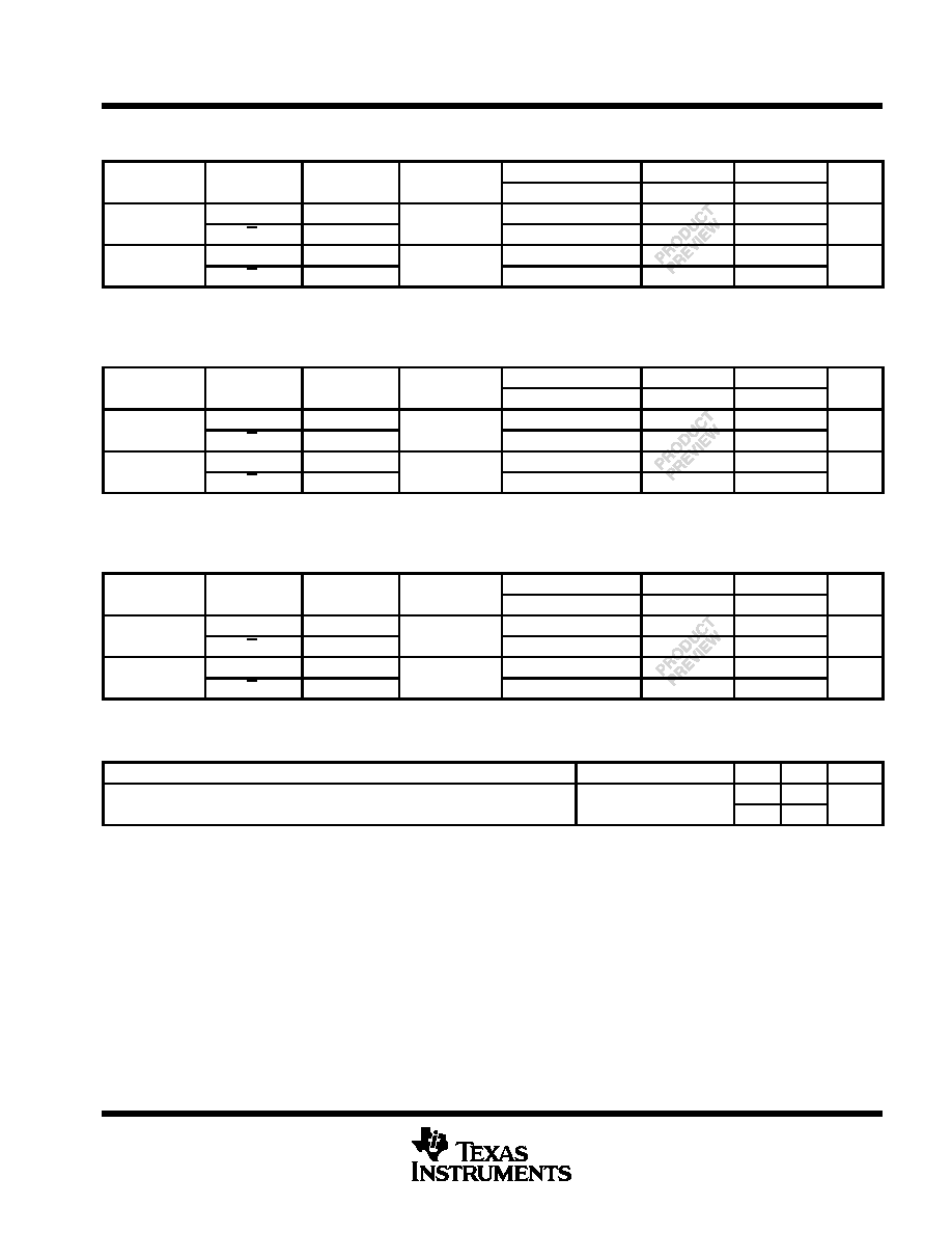
switching characteristics over recommended operating free-air temperature range,
V
CC
= 2.5 V
±
0.2 V (unless otherwise noted) (see Figure 1)
PARAMETER
FROM
TO
LOAD
TA = 25
∞
C
SN54LV139A
SN74LV139A
UNIT
PARAMETER
(INPUT)
(OUTPUT)
CAPACITANCE
MIN
TYP
MAX
MIN
MAX
MIN
MAX
UNIT
t d
A or B
Y
CL = 15 pF
7.7*
17.6*
1*
21*
1
21
ns
tpd
G
Y
CL = 15 pF
7.4*
15.8*
1*
19*
1
19
ns
t d
A or B
Y
CL = 50 pF
10.2
22.5
1
26.5
1
26.5
ns
tpd
G
Y
CL = 50 pF
9.9
20.2
1
24
1
24
ns
* On products compliant to MIL-PRF-38535, this parameter is not production tested.
switching characteristics over recommended operating free-air temperature range,
V
CC
= 3.3 V
±
0.3 V (unless otherwise noted) (see Figure 1)
PARAMETER
FROM
TO
LOAD
TA = 25
∞
C
SN54LV139A
SN74LV139A
UNIT
PARAMETER
(INPUT)
(OUTPUT)
CAPACITANCE
MIN
TYP
MAX
MIN
MAX
MIN
MAX
UNIT
t d
A or B
Y
CL = 15 pF
5.3*
11*
1*
13*
1
13
ns
tpd
G
Y
CL = 15 pF
5.1*
9.2*
1*
11*
1
11
ns
t d
A or B
Y
CL = 50 pF
7.3
14.5
1
16.5
1
16.5
ns
tpd
G
Y
CL = 50 pF
7
12.7
1
14.5
1
14.5
ns
* On products compliant to MIL-PRF-38535, this parameter is not production tested.
switching characteristics over recommended operating free-air temperature range,
V
CC
= 5 V
±
0.5 V (unless otherwise noted) (see Figure 1)
PARAMETER
FROM
TO
LOAD
TA = 25
∞
C
SN54LV139A
SN74LV139A
UNIT
PARAMETER
(INPUT)
(OUTPUT)
CAPACITANCE
MIN
TYP
MAX
MIN
MAX
MIN
MAX
UNIT
t d
A or B
Y
CL = 15 pF
3.7*
7.2*
1*
8.5*
1
8.5
ns
tpd
G
Y
CL = 15 pF
3.5*
6.3*
1*
7.5*
1
7.5
ns
t d
A or B
Y
CL = 50 pF
5.2
9.2
1
10.5
1
10.5
ns
tpd
G
Y
CL = 50 pF
4.9
8.3
1
9.5
1
9.5
ns
* On products compliant to MIL-PRF-38535, this parameter is not production tested.
operating characteristics, T
A
= 25
∞
C
PARAMETER
TEST CONDITIONS
VCC
TYP
UNIT
C d
Power dissipation capacitance
CL = 50 pF
f = 10 MHz
3.3 V
17.3
pF
Cpd
Power dissipation capacitance
CL = 50 pF,
f = 10 MHz
5 V
18.2
pF
PRODUCT PREVIEW information concerns products in the formative or
design phase of development. Characteristic data and other
specifications are design goals. Texas Instruments reserves the right to
change or discontinue these products without notice.