SN74LVC16374
16-BIT EDGE-TRIGGERED D-TYPE FLIP-FLOP
WITH 3-STATE OUTPUTS
SCAS316B ≠ NOVEMBER 1993 ≠ REVISED JULY 1995
1
POST OFFICE BOX 655303
∑
DALLAS, TEXAS 75265
D
Member of the Texas Instruments
Widebus
TM
Family
D
EPIC
TM
(Enhanced-Performance Implanted
CMOS) Submicron Process
D
Typical V
OLP
(Output Ground Bounce)
< 0.8 V at V
CC
= 3.3 V, T
A
= 25
∞
C
D
Typical V
OHV
(Output V
OH
Undershoot)
> 2 V at V
CC
= 3.3 V, T
A
= 25
∞
C
D
Latch-Up Performance Exceeds 250 mA
Per JEDEC Standard JESD-17
D
Bus Hold on Data Inputs Eliminates the
Need for External Pullup/Pulldown
Resistors
D
Package Options Include Plastic 300-mil
Shrink Small-Outline (DL) and Thin Shrink
Small-Outline (DGG) Packages
description
This 16-bit edge-triggered D-type flip-flop is
designed for 2.7-V to 3.6-V V
CC
operation.
The SN74LVC16374 is particularly suitable for
implementing buffer registers, I/O ports,
bidirectional bus drivers, and working registers. It
can be used as two 8-bit flip-flops or one 16-bit
flip-flop. On the positive transition of the clock
(CLK) input, the Q outputs of the flip-flop take on
the logic levels set up at the data (D) inputs.
A buffered output-enable (OE) input can be used to place the eight outputs in either a normal logic state (high
or low logic levels) or a high-impedance state. In the high-impedance state, the outputs neither load nor drive
the bus lines significantly. The high-impedance state and the increased drive provide the capability to drive bus
lines without need for interface or pullup components.
OE does not affect internal operations of the flip-flop. Old data can be retained or new data can be entered while
the outputs are in the high-impedance state.
To ensure the high-impedance state during power up or power down, OE should be tied to V
CC
through a pullup
resistor; the minimum value of the resistor is determined by the current-sinking capability of the driver.
Active bus-hold circuitry is provided to hold unused or floating data inputs at a valid logic level.
The SN74LVC16374 is characterized for operation from ≠ 40
∞
C to 85
∞
C.
Copyright
©
1995, Texas Instruments Incorporated
PRODUCTION DATA information is current as of publication date.
Products conform to specifications per the terms of Texas Instruments
standard warranty. Production processing does not necessarily include
testing of all parameters.
EPIC and Widebus are trademarks of Texas Instruments Incorporated.
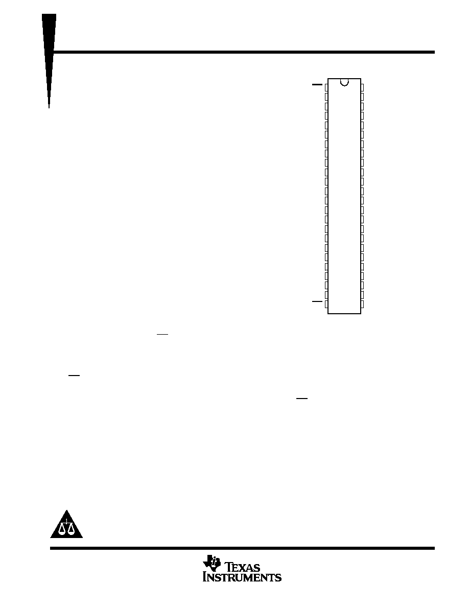
DGG OR DL PACKAGE
(TOP VIEW)
1
2
3
4
5
6
7
8
9
10
11
12
13
14
15
16
17
18
19
20
21
22
23
24
48
47
46
45
44
43
42
41
40
39
38
37
36
35
34
33
32
31
30
29
28
27
26
25
1OE
1Q1
1Q2
GND
1Q3
1Q4
V
CC
1Q5
1Q6
GND
1Q7
1Q8
2Q1
2Q2
GND
2Q3
2Q4
V
CC
2Q5
2Q6
GND
2Q7
2Q8
2OE
1CLK
1D1
1D2
GND
1D3
1D4
V
CC
1D5
1D6
GND
1D7
1D8
2D1
2D2
GND
2D3
2D4
V
CC
2D5
2D6
GND
2D7
2D8
2CLK
Please be aware that an important notice concerning availability, standard warranty, and use in critical applications of
Texas Instruments semiconductor products and disclaimers thereto appears at the end of this data sheet.
SN74LVC16374
16-BIT EDGE-TRIGGERED D-TYPE FLIP-FLOP
WITH 3-STATE OUTPUTS
SCAS316B ≠ NOVEMBER 1993 ≠ REVISED JULY 1995
2
POST OFFICE BOX 655303
∑
DALLAS, TEXAS 75265
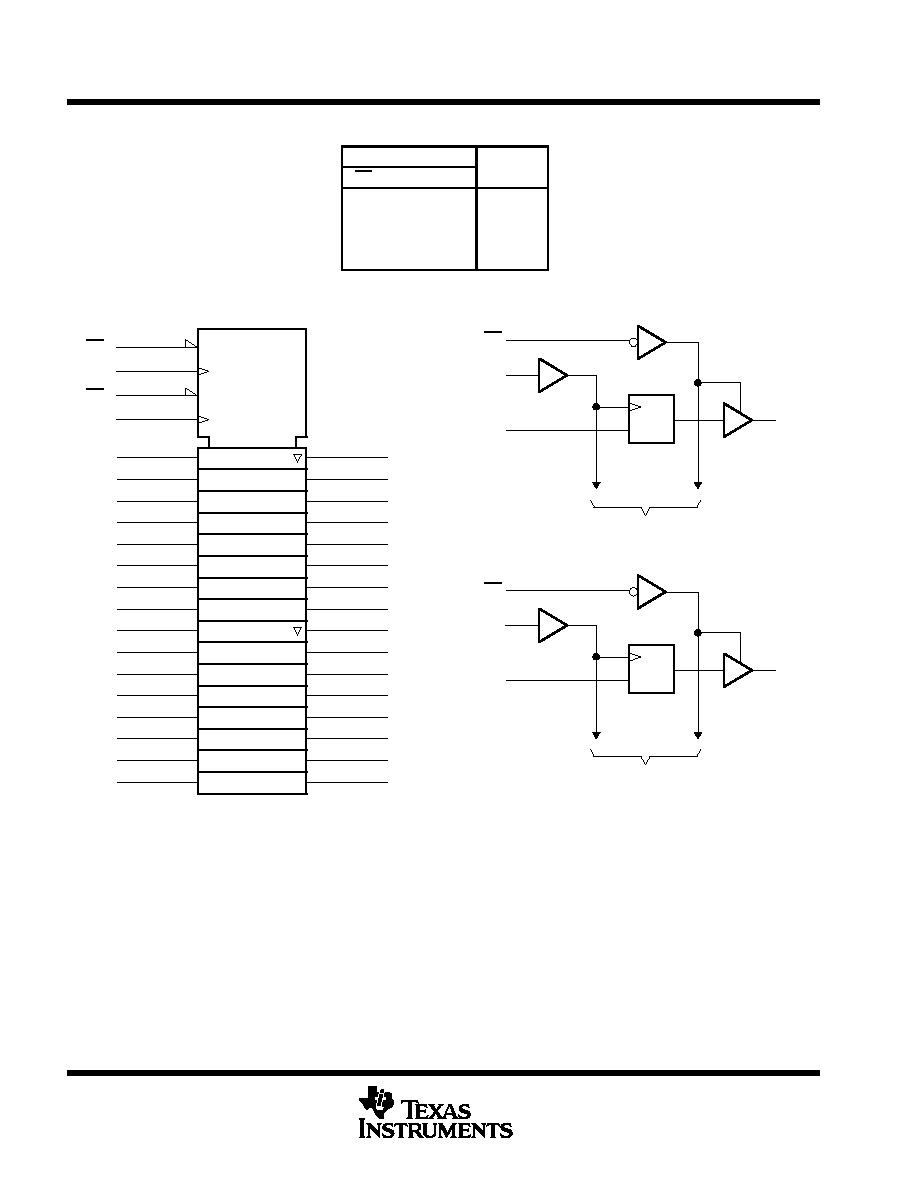
FUNCTION TABLE
(each flip-flop)
INPUTS
OUTPUT
OE
CLK
D
Q
L
H
H
L
L
L
L
H or L
X
Q0
H
X
X
Z
logic symbol
logic diagram (positive logic)
1OE
2OE
48
47
1OE
1
1CLK
1D1
To Seven Other Channels
2
1Q1
C1
1D
25
36
2OE
24
2CLK
2D1
13
2Q1
C1
1D
To Seven Other Channels
1EN
1
48
1CLK
1D
47
1D1
46
1D2
44
1D3
43
1D4
1Q1
2
1Q2
3
1Q3
5
1Q4
6
1
41
1D5
40
1D6
38
1D7
37
1D8
1Q5
8
1Q6
9
1Q7
11
1Q8
12
2D
36
2D1
35
2D2
33
2D3
32
2D4
2Q1
13
2Q2
14
2Q3
16
2Q4
17
30
2D5
29
2D6
27
2D7
26
2D8
2Q5
19
2Q6
20
2Q7
22
2Q8
23
2
2EN
24
25
2CLK
C1
C2
This symbol is in accordance with ANSI/IEEE Std 91-1984
and IEC Publication 617-12.
SN74LVC16374
16-BIT EDGE-TRIGGERED D-TYPE FLIP-FLOP
WITH 3-STATE OUTPUTS
SCAS316B ≠ NOVEMBER 1993 ≠ REVISED JULY 1995
3
POST OFFICE BOX 655303
∑
DALLAS, TEXAS 75265
absolute maximum ratings over operating free-air temperature range (unless otherwise noted)
Supply voltage range, V
CC
≠ 0.5 V to 4.6 V
. . . . . . . . . . . . . . . . . . . . . . . . . . . . . . . . . . . . . . . . . . . . . . . . . . . . . . . .
Input voltage range, V
I
(see Note 1)
≠ 0.5 V to 4.6 V
. . . . . . . . . . . . . . . . . . . . . . . . . . . . . . . . . . . . . . . . . . . . . . . .
Output voltage range, V
O
(see Notes 1 and 2)
≠ 0.5 V to V
CC
+ 0.5 V
. . . . . . . . . . . . . . . . . . . . . . . . . . . . . . . . .
Input clamp current, I
IK
(V
I
< 0)
≠ 50 mA
. . . . . . . . . . . . . . . . . . . . . . . . . . . . . . . . . . . . . . . . . . . . . . . . . . . . . . . . . .
Output clamp current, I
OK
(V
O
< 0 or V
O
> V
CC
)
±
50 mA
. . . . . . . . . . . . . . . . . . . . . . . . . . . . . . . . . . . . . . . . . . .
Continuous output current, I
O
(V
O
= 0 to V
CC
)
±
50 mA
. . . . . . . . . . . . . . . . . . . . . . . . . . . . . . . . . . . . . . . . . . . . .
Continuous current through V
CC
or GND
±
100 mA
. . . . . . . . . . . . . . . . . . . . . . . . . . . . . . . . . . . . . . . . . . . . . . . . .
Maximum power dissipation at T
A
= 55
∞
C (in still air) (see Note 3): DGG package
0.85 W
. . . . . . . . . . . . . . .
DL package
1.2 W
. . . . . . . . . . . . . . . . . .
Storage temperature range, T
stg
≠ 65
∞
C to 150
∞
C
. . . . . . . . . . . . . . . . . . . . . . . . . . . . . . . . . . . . . . . . . . . . . . . . . .
Stresses beyond those listed under "absolute maximum ratings" may cause permanent damage to the device. These are stress ratings only, and
functional operation of the device at these or any other conditions beyond those indicated under "recommended operating conditions" is not
implied. Exposure to absolute-maximum-rated conditions for extended periods may affect device reliability.
NOTES:
1. The input and output negative-voltage ratings may be exceeded if the input and output clamp-current ratings are observed.
2. This value is limited to 4.6 V maximum.
3. The maximum package power dissipation is calculated using a junction temperature of 150
∞
C and a board trace length of 750 mils.
For more information, refer to the
Package Thermal Considerations application note in the 1994 ABT Advanced BiCMOS Technology
Data Book, literature number SCBD002B.
recommended operating conditions (see Note 4)
MIN
MAX
UNIT
VCC
Supply voltage
2.7
3.6
V
VIH
High-level input voltage
VCC = 2.7 V to 3.6 V
2
V
VIL
Low-level input voltage
VCC = 2.7 V to 3.6 V
0.8
V
VI
Input voltage
0
VCC
V
VO
Output voltage
0
VCC
V
IOH
High level output current
VCC = 2.7 V
≠ 12
mA
IOH
High-level output current
VCC = 3 V
≠ 24
mA
IOL
Low level output current
VCC = 2.7 V
12
mA
IOL
Low-level output current
VCC = 3 V
24
mA
t /
v
Input transition rise or fall rate
0
10
ns / V
TA
Operating free-air temperature
≠ 40
85
∞
C
NOTE 4: Unused control inputs must be held high or low to prevent them from floating.

SN74LVC16374
16-BIT EDGE-TRIGGERED D-TYPE FLIP-FLOP
WITH 3-STATE OUTPUTS
SCAS316B ≠ NOVEMBER 1993 ≠ REVISED JULY 1995
4
POST OFFICE BOX 655303
∑
DALLAS, TEXAS 75265
electrical characteristics over recommended operating free-air temperature range (unless
otherwise noted)
PARAMETER
TEST CONDITIONS
VCC
MIN
TYP
MAX
UNIT
IOH = ≠ 100
µ
A
MIN to MAX
VCC ≠ 0.2
VOH
IOH = 12 mA
2.7 V
2.2
V
VOH
IOH = ≠ 12 mA
3 V
2.4
V
IOH = ≠ 24 mA
3 V
2
IOL = 100
µ
A
MIN to MAX
0.2
VOL
IOL = 12 mA
2.7 V
0.4
V
IOL = 24 mA
3 V
0.55
II
VI = VCC or GND
3.6 V
±
5
µ
A
VI = 0.8 V
3 V
75
II(hold)
Data inputs
VI = 2 V
3 V
≠75
µ
A
(
)
VI = 0 to 3.6 V
3.6 V
±
500
IOZ
VO = VCC or GND
3.6 V
±
10
µ
A
ICC
VI = VCC or GND,
IO = 0
3.6 V
40
µ
A
n
ICC
One input at VCC ≠ 0.6 V,
Other inputs at VCC or GND
3 V to 3.6 V
500
µ
A
Ci
VI = VCC or GND
3.3 V
3.5
pF
Co
VO = VCC or GND
3.3 V
7
pF
For conditions shown as MIN or MAX, use the appropriate values under recommended operating conditions.
All typical values are at VCC = 3.3 V, TA = 25
∞
C.
timing requirements over recommended operating free-air temperature range (unless otherwise
noted)
VCC = 3.3 V
±
0.3 V
VCC = 2.7 V
UNIT
MIN
MAX
MIN
MAX
fclock
Clock frequency
0
100
0
80
MHz
tw
Pulse duration, CLK high or low
4
4
ns
tsu
Setup time, data before CLK
High or low
2
3
ns
th
Hold time, data after CLK
High or low
1.5
1.5
ns
switching characteristics over recommended operating free-air temperature range, C
L
= 50 pF
(unless otherwise noted) (see Figure 1)
PARAMETER
FROM
(INPUT)
TO
(OUTPUT)
VCC = 3.3 V
±
0.3 V
VCC = 2.7 V
UNIT
(INPUT)
(OUTPUT)
MIN
MAX
MIN
MAX
fmax
100
80
MHz
tpd
CLK
Q
1.5
7.5
1.5
8.5
ns
ten
OE
Q
1.5
7.5
1.5
8.5
ns
tdis
OE
Q
1.5
7
1.5
8
ns

SN74LVC16374
16-BIT EDGE-TRIGGERED D-TYPE FLIP-FLOP
WITH 3-STATE OUTPUTS
SCAS316B ≠ NOVEMBER 1993 ≠ REVISED JULY 1995
5
POST OFFICE BOX 655303
∑
DALLAS, TEXAS 75265
operating characteristics, V
CC
= 3.3 V, T
A
= 25
∞
C
PARAMETER
TEST CONDITIONS
TYP
UNIT
C d
Power dissipation capacitance per flip flop
Outputs enabled
CL = 50 pF f = 10 MHz
22
pF
Cpd
Power dissipation capacitance per flip-flop
Outputs disabled
CL = 50 pF, f = 10 MHz
9
pF
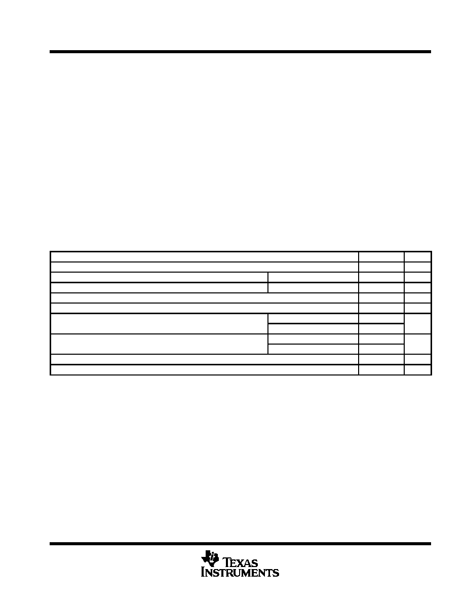
PARAMETER MEASUREMENT INFORMATION
500
1.5 V
th
tsu
From Output
Under Test
CL = 50 pF
(see Note A)
LOAD CIRCUIT FOR OUTPUTS
S1
6 V
Open
GND
500
Data Input
Timing Input
1.5 V
2.7 V
0 V
1.5 V
1.5 V
2.7 V
0 V
2.7 V
0 V
1.5 V
1.5 V
tw
Input
VOLTAGE WAVEFORMS
SETUP AND HOLD TIMES
VOLTAGE WAVEFORMS
PROPAGATION DELAY TIMES
INVERTING AND NONINVERTING OUTPUTS
VOLTAGE WAVEFORMS
PULSE DURATION
tPLH
tPHL
tPHL
tPLH
VOH
VOH
VOL
VOL
1.5 V
1.5 V
2.7 V
0 V
1.5 V
1.5 V
Input
1.5 V
Output
Control
Output
Waveform 1
S1 at 6 V
(see Note B)
Output
Waveform 2
S1 at GND
(see Note B)
VOL
VOH
tPZL
tPZH
tPLZ
tPHZ
1.5 V
1.5 V
3 V
0 V
1.5 V
VOL + 0.3 V
1.5 V
VOH ≠ 0.3 V
[
0 V
2.7 V
VOLTAGE WAVEFORMS
ENABLE AND DISABLE TIMES
LOW- AND HIGH-LEVEL ENABLING
Output
Output
tpd
tPLZ/tPZL
tPHZ/tPZH
Open
6 V
GND
TEST
S1
NOTES: A. CL includes probe and jig capacitance.
B. Waveform 1 is for an output with internal conditions such that the output is low except when disabled by the output control.
Waveform 2 is for an output with internal conditions such that the output is high except when disabled by the output control.
C. All input pulses are supplied by generators having the following characteristics: PRR
10 MHz, ZO = 50
, tr
2.5 ns, tf
2.5 ns.
D. The outputs are measured one at a time with one transition per measurement.
E. tPLZ and tPHZ are the same as tdis.
F. tPZL and tPZH are the same as ten.
G. tPLH and tPHL are the same as tpd.
Figure 1. Load Circuit and Voltage Waveforms