SN65ALS176, SN75ALS176, SN75ALS176A, SN75ALS176B
DIFFERENTIAL BUS TRANSCEIVERS
SLLS040G ≠ AUGUST 1987 ≠ REVISED DECEMBER 1999
1
POST OFFICE BOX 655303
∑
DALLAS, TEXAS 75265
D
Meet or Exceed the Requirements of
TIA/EIA-422-B, TIA/EIA-485-A, and ITU
Recommendations V.11 and X.27
D
Operate at Data Rates up to 35 MBaud
D
Four Skew Limits Available:
SN65ALS176 . . . 15 ns
SN75ALS176 . . . 10 ns
SN75ALS176A . . . 7.5 ns
SN75ALS176B . . . 5 ns
D
Designed for Multipoint Transmission on
Long Bus Lines in Noisy Environments
D
Low Supply-Current Requirements . . .
30 mA Max
D
Wide Positive and Negative Input/Output
Bus-Voltage Ranges
D
Thermal Shutdown Protection
D
Driver Positive and Negative Current
Limiting
D
Receiver Input Hysteresis
D
Glitch-Free Power-Up and Power-Down
Protection
D
Receiver Open-Circuit Fail-Safe Design
description
The SN65ALS176 and SN75ALS176 series differential bus transceivers are designed for bidirectional data
communication on multipoint bus transmission lines. They are designed for balanced transmission lines and
meet TIA/EIA-422-B, TIA/EIA-485-A, and ITU Recommendations V.11 and X.27.
The SN65ALS176 and SN75ALS176 series combine a 3-state, differential line driver and a differential input line
receiver, both of which operate from a single 5-V power supply. The driver and receiver have active-high and
active-low enables, respectively, that can be connected together externally to function as a direction control.
The driver differential outputs and the receiver differential inputs are connected internally to form a differential
input/output (I/O) bus port that is designed to offer minimum loading to the bus when the driver is disabled or
V
CC
= 0. This port features wide positive and negative common-mode voltage ranges, making the device
suitable for party-line applications.
The SN65ALS176 is characterized for operation from ≠ 40
∞
C to 85
∞
C, and the SN75ALS176 series is
characterized for operation from 0
∞
C to 70
∞
C.
Copyright
©
1999, Texas Instruments Incorporated
PRODUCTION DATA information is current as of publication date.
Products conform to specifications per the terms of Texas Instruments
standard warranty. Production processing does not necessarily include
testing of all parameters.
Please be aware that an important notice concerning availability, standard warranty, and use in critical applications of
Texas Instruments semiconductor products and disclaimers thereto appears at the end of this data sheet.
1
2
3
4
8
7
6
5
R
RE
DE
D
V
CC
B
A
GND
D OR P PACKAGE
(TOP VIEW)
SN65ALS176, SN75ALS176, SN75ALS176A, SN75ALS176B
DIFFERENTIAL BUS TRANSCEIVERS
SLLS040G ≠ AUGUST 1987 ≠ REVISED DECEMBER 1999
2
POST OFFICE BOX 655303
∑
DALLAS, TEXAS 75265
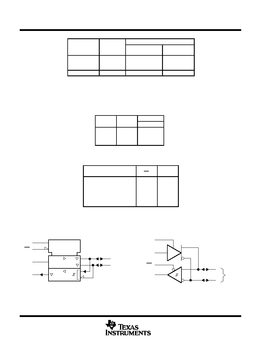
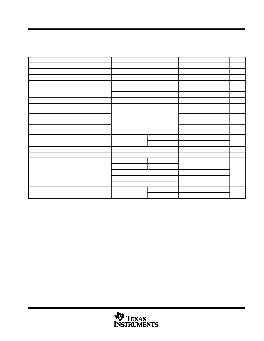
AVAILABLE OPTIONS
PACKAGED DEVICES
TA
tsk(lim)
SMALL OUTLINE
(D)
PLASTIC DIP
(P)
0
∞
C to 70
∞
C
10
7.5
5
SN75ALS176D
SN75ALS176AD
SN75ALS176BD
SN75ALS176P
SN75ALS176AP
SN75ALS176BP
≠ 40
∞
C to 85
∞
C
15
SN65ALS176D
SN65ALS176P
tsk(lim) This is the maximum range that the driver or receiver delay times vary
over temperature, VCC, and process (device to device).
The D package is available taped and reeled. Add the suffix R to the device type
(e.g., SN75ALS176DR).
Function Tables
DRIVER
INPUT
ENABLE
OUTPUTS
D
DE
A
B
H
H
H
L
L
H
L
H
X
L
Z
Z
H = high level, L = low level, X = irrelevant,
Z = high impedance
RECEIVER
DIFFERENTIAL INPUTS
ENABLE
OUTPUT
A≠B
RE
R
VID
0.2 V
L
H
≠ 0.2 V < VID < 0.2 V
L
?
VID
≠ 0.2 V
L
L
X
H
Z
Inputs open
L
H
H = high level, L = low level, X = irrelevant,
Z = high impedance
logic symbol
ß
R
D
RE
DE
1
4
2
3
EN2
EN1
B
A
7
6
2
1
1
ß This symbol is in accordance with ANSI/IEEE Std 91-1984
and IEC Publication 617-12.
logic diagram (positive logic)
Bus
B
7
A
6
1
R
2
RE
3
DE
4
D
SN65ALS176, SN75ALS176, SN75ALS176A, SN75ALS176B
DIFFERENTIAL BUS TRANSCEIVERS
SLLS040G ≠ AUGUST 1987 ≠ REVISED DECEMBER 1999
3
POST OFFICE BOX 655303
∑
DALLAS, TEXAS 75265
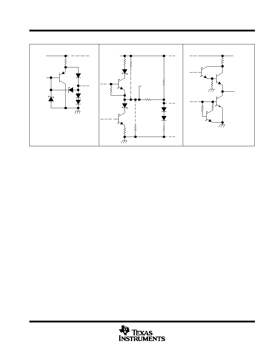
schematics of inputs and outputs
EQUIVALENT OF EACH INPUT
Driver Input: R(eq) = 3 k
NOM
Enable Inputs: R(eq) = 8 k
NOM
R(eq) = equivalent resistor
TYPICAL OF A AND B I/O PORTS
TYPICAL OF RECEIVER OUTPUT
Output
85
NOM
VCC
180 k
NOM
Connected
on B Port
1.1 k
NOM
3 k
NOM
18 k
NOM
Connected
on A Port
180 k
NOM
A or B
R(eq)
VCC
Input
VCC
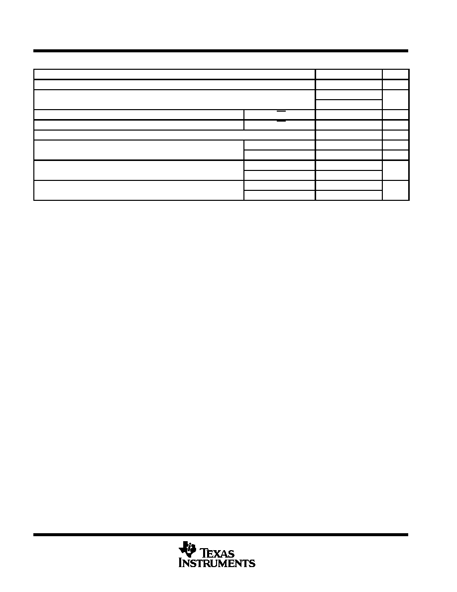
absolute maximum ratings over operating free-air temperature range (unless otherwise noted)
Supply voltage, V
CC
(see Note 1)
7 V
. . . . . . . . . . . . . . . . . . . . . . . . . . . . . . . . . . . . . . . . . . . . . . . . . . . . . . . . . . . . .
Voltage range at any bus terminal
≠ 7 V to 12 V
. . . . . . . . . . . . . . . . . . . . . . . . . . . . . . . . . . . . . . . . . . . . . . . . . . . . .
Enable input voltage, V
I
5.5 V
. . . . . . . . . . . . . . . . . . . . . . . . . . . . . . . . . . . . . . . . . . . . . . . . . . . . . . . . . . . . . . . . . . . .
Package thermal impedance,
JA
(see Note 2): D package
197
∞
C/W
. . . . . . . . . . . . . . . . . . . . . . . . . . . . . . . . .
P package
104
∞
C/W
. . . . . . . . . . . . . . . . . . . . . . . . . . . . . . . . . .
Lead temperature 1,6 mm (1/16 inch) from case for 10 seconds
260
∞
C
. . . . . . . . . . . . . . . . . . . . . . . . . . . . . . .
Storage temperature range, T
stg
≠ 65
∞
C to 150
∞
C
. . . . . . . . . . . . . . . . . . . . . . . . . . . . . . . . . . . . . . . . . . . . . . . . . . .
Stresses beyond those listed under "absolute maximum ratings" may cause permanent damage to the device. These are stress ratings only, and
functional operation of the device at these or any other conditions beyond those indicated under "recommended operating conditions" is not
implied. Exposure to absolute-maximum-rated conditions for extended periods may affect device reliability.
NOTES:
1. All voltage values, except differential I/O bus voltage, are with respect to network ground terminal.
2. The package thermal impedance is calculated in accordance with JESD 51.
SN65ALS176, SN75ALS176, SN75ALS176A, SN75ALS176B
DIFFERENTIAL BUS TRANSCEIVERS
SLLS040G ≠ AUGUST 1987 ≠ REVISED DECEMBER 1999
4
POST OFFICE BOX 655303
∑
DALLAS, TEXAS 75265
recommended operating conditions (unless otherwise noted)
MIN
NOM
MAX
UNIT
Supply voltage, VCC
4.75
5
5.25
V
Input voltage at any bus terminal (separately or common mode) VI or VIC
12
V
Input voltage at any bus terminal (separately or common mode), VI or VIC
≠ 7
V
High-level input voltage, VIH
D, DE, and RE
2
V
Low-level input voltage, VIL
D, DE, and RE
0.8
V
Differential input voltage, VID (see Note 3)
±
12
V
High level output current IOH
Driver
≠ 60
mA
High-level output current, IOH
Receiver
≠ 400
µ
A
Low level output current IOL
Driver
60
mA
Low-level output current, IOL
Receiver
8
mA
Operating free air temperature TA
SN65ALS176
≠ 40
85
∞
C
Operating free-air temperature, TA
SN75ALS176 series
0
70
∞
C
NOTE 3: Differential input/output bus voltage is measured at the noninverting terminal A with respect to the inverting terminal B.
SN65ALS176, SN75ALS176, SN75ALS176A, SN75ALS176B
DIFFERENTIAL BUS TRANSCEIVERS
SLLS040G ≠ AUGUST 1987 ≠ REVISED DECEMBER 1999
5
POST OFFICE BOX 655303
∑
DALLAS, TEXAS 75265
DRIVER SECTION
electrical characteristics over recommended ranges of supply voltage and operating free-air
temperature range (unless otherwise noted)
PARAMETER
TEST CONDITIONS
MIN
TYP
MAX
UNIT
VIK
Input clamp voltage
II = ≠ 18 mA
≠ 1.5
V
VO
Output voltage
IO = 0
0
6
V
| VOD1 |
Differential output voltage
IO = 0
1.5
6
V
| VOD2 |
Differential output voltage
RL = 100
,
See Figure 1
1/2 VOD1
or 2ß
V
OD2
g
RL = 54
,
See Figure 1
1.5
2.5
5
V
VOD3
Differential output voltage
Vtest = ≠ 7 V to 12 V,
See Figure 2
1.5
5
V
| VOD |
Change in magnitude of differential
output voltage ∂
±
0.2
V
VOC
Common mode output voltage
RL = 54
or 100
See Figure 1
3
V
VOC
Common-mode output voltage
RL = 54
or 100
,
See Figure 1
≠ 1
V
| VOC |
Change in magnitude of
common-mode output voltage∂
±
0.2
V
IO
Output current
Outputs disabled,
VO = 12 V
1
mA
IO
Output current
,
See Note 4
VO = ≠ 7 V
≠ 0.8
mA
IIH
High-level input current
VI = 2.4 V
20
µ
A
IIL
Low-level input current
VI = 0.4 V
≠ 400
µ
A
#
VO = ≠ 4 V
SN65ALS176
250
#
VO = ≠ 6 V
SN75ALS176
≠ 250
IOS
Short-circuit output current#
VO = 0
≠ 150
mA
VO = VCC
250
VO = 8 V
250
ICC
Supply current
No load
Outputs enabled
23
30
mA
ICC
Supply current
No load
Outputs disabled
19
26
mA
The power-off measurement in TIA/EIA-422-B applies to disabled outputs only and is not applied to combined inputs and outputs.
All typical values are at VCC = 5 V and TA = 25
∞
C.
ß The minimum VOD2 with a 100-
load is either 1/2 VOD1 or 2 V, whichever is greater.
∂
| VOD | and
| VOC | are the changes in magnitude of VOD and VOC, respectively, that occur when the input is changed from one logic state
to the other.
# Duration of the short circuit should not exceed one second for this test.
NOTE 4: This applies for power on and power off. Refer to TIA/EIA-485-A for exact conditions. The TIA/EIA-422-B limit does not apply for a
combined driver and receiver terminal.