
SN65C3221, SN75C3221
3 V TO 5.5 V SINGLE CHANNEL RS 232 COMPATIBLE LINE DRIVER/RECEIVER
SLLS351E - APRIL 2002 - REVISED OCTOBER 2004
1
POST OFFICE BOX 655303
∑
DALLAS, TEXAS 75265
D
Operate With 3-V to 5.5-V V
CC
Supply
D
Operate Up To 1 Mbit/s
D
Low Standby Current . . . 1
µ
A Typ
D
External Capacitors . . . 4
◊
0.1
µ
F
D
Accepts 5-V Logic Input With 3.3-V Supply
D
RS-232 Bus-Pin ESD Protection Exceeds
±
15 kV Using Human-Body Model (HBM)
D
Auto-Powerdown Feature Automatically
Disables Drivers for Power Savings
D
Applications
- Battery-Powered, Hand-Held, and
Portable Equipment
- PDAs and Palmtop PCs
- Notebooks, Sub-Notebooks, and Laptops
- Digital Cameras
- Mobile Phones and Wireless Devices
description/ordering information
The SN65C3221 and SN75C3221 consist of one line driver, one line receiver, and a dual charge-pump circuit
with
±
15-kV ESD protection pin to pin (serial-port connection pins, including GND). These devices provide the
electrical interface between an asynchronous communication controller and the serial-port connector. The
charge pump and four small external capacitors allow operation from a single 3-V to 5.5-V supply. These devices
operate at data signaling rates up to 1 Mbit/s and a driver output slew rate of 24 V/
µ
s to 150 V/
µ
s.
Flexible control options for power management are available when the serial port is inactive. The
auto-powerdown feature functions when FORCEON is low and FORCEOFF is high. During this mode of
operation, if the devices do not sense a valid RS-232 signal on the receiver input, the driver output is disabled.
If FORCEOFF is set low and EN is high, both the driver and receiver are shut off, and the supply current is
reduced to 1
µ
A. Disconnecting the serial port or turning off the peripheral drivers causes the auto-powerdown
condition to occur. Auto-powerdown can be disabled when FORCEON and FORCEOFF are high. With
auto-powerdown enabled, the device is activated automatically when a valid signal is applied to the receiver
input. The INVALID output notifies the user if an RS-232 signal is present at the receiver input. INVALID is high
(valid data) if the receiver input voltage is greater than 2.7 V or less than -2.7 V, or has been between -0.3 V
and 0.3 V for less than 30
µ
s. INVALID is low (invalid data) if the receiver input voltage is between -0.3 V and
0.3 V for more than 30
µ
s. Refer to Figure 5 for receiver input levels.
ORDERING INFORMATION
TA
PACKAGE
ORDERABLE
PART NUMBER
TOP-SIDE
MARKING
SSOP (DB)
Reel of 2000
SN75C3221DBR
CA3221
-0
∞
C to 70
∞
C
TSSOP (PW)
Tube of 90
SN75C3221PW
CA3221
-0 C to 70 C
TSSOP (PW)
Reel of 2000
SN75C3221PWR
CA3221
SSOP (DB)
Reel of 2000
SN65C3221DBR
CB3221
-40
∞
C to 85
∞
C
TSSOP (PW)
Tube of 90
SN65C3221PW
CB3221
-40 C to 85 C
TSSOP (PW)
Reel of 2000
SN65C3221PWR
CB3221
Package drawings, standard packing quantities, thermal data, symbolization, and PCB design guidelines are
available at www.ti.com/sc/package.
Copyright
2004, Texas Instruments Incorporated
Please be aware that an important notice concerning availability, standard warranty, and use in critical applications of
Texas Instruments semiconductor products and disclaimers thereto appears at the end of this data sheet.
DB OR PW PACKAGE
(TOP VIEW)
1
2
3
4
5
6
7
8
16
15
14
13
12
11
10
9
EN
C1+
V+
C1-
C2+
C2-
V-
RIN
FORCEOFF
V
CC
GND
DOUT
FORCEON
DIN
INVALID
ROUT
PRODUCTION DATA information is current as of publication date.
Products conform to specifications per the terms of Texas Instruments
standard warranty. Production processing does not necessarily include
testing of all parameters.

SN65C3221, SN75C3221
3 V TO 5.5 V SINGLE CHANNEL RS 232 COMPATIBLE LINE DRIVER/RECEIVER
SLLS351E - APRIL 2002 - REVISED OCTOBER 2004
2
POST OFFICE BOX 655303
∑
DALLAS, TEXAS 75265
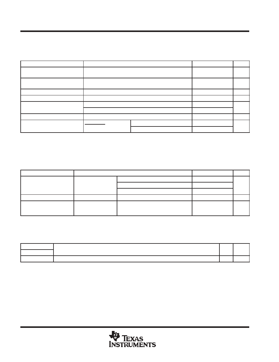
Function Tables
EACH DRIVER
INPUTS
OUTPUT
DIN
FORCEON
FORCEOFF
VALID RIN
RS-232 LEVEL
OUTPUT
DOUT
DRIVER STATUS
X
X
L
X
Z
Powered off
L
H
H
X
H
Normal operation with
H
H
H
X
L
Normal operation with
auto-powerdown disabled
L
L
H
Yes
H
Normal operation with
H
L
H
Yes
L
Normal operation with
auto-powerdown enabled
L
L
H
No
Z
Powered off by
H
L
H
No
Z
Powered off by
auto-powerdown feature
H = high level, L = low level, X = irrelevant, Z = high impedance
EACH RECEIVER
INPUTS
OUTPUT
RIN
EN
VALID RIN
RS-232 LEVEL
OUTPUT
ROUT
L
L
X
H
H
L
X
L
X
H
X
Z
Open
L
No
H
H = high level, L = low level, X = irrelevant,
Z = high impedance (off), Open = disconnected
input or connected driver off
logic diagram (positive logic)
DIN
DOUT
Auto-powerdown
INVALID
RIN
FORCEOFF
FORCEON
ROUT
EN
11
16
9
13
10
8
1
12

SN65C3221, SN75C3221
3 V TO 5.5 V SINGLE CHANNEL RS 232 COMPATIBLE LINE DRIVER/RECEIVER
SLLS351E - APRIL 2002 - REVISED OCTOBER 2004
3
POST OFFICE BOX 655303
∑
DALLAS, TEXAS 75265
absolute maximum ratings over operating free-air temperature range (unless otherwise noted)
Supply voltage range, V
CC
(see Note 1)
-0.3 V to 6 V
. . . . . . . . . . . . . . . . . . . . . . . . . . . . . . . . . . . . . . . . . . . . . .
Positive output supply voltage range, V+ (see Note 1)
-0.3 V to 7 V
. . . . . . . . . . . . . . . . . . . . . . . . . . . . . . . . . .
Negative output supply voltage range, V- (see Note 1)
0.3 V to -7 V
. . . . . . . . . . . . . . . . . . . . . . . . . . . . . . . . .
Supply voltage difference, V+
-
V- (see Note 1)
13 V
. . . . . . . . . . . . . . . . . . . . . . . . . . . . . . . . . . . . . . . . . . . . . . .
Input voltage range, V
I
: Driver (FORCEOFF, FORCEON, EN)
-0.3 V to 6 V
. . . . . . . . . . . . . . . . . . . . . . . . . . .
Receiver
-25 V to 25 V
. . . . . . . . . . . . . . . . . . . . . . . . . . . . . . . . . . . . . . . . . . . . . . . . . . . .
Output voltage range, V
O
: Driver
-13.2 V to 13.2 V
. . . . . . . . . . . . . . . . . . . . . . . . . . . . . . . . . . . . . . . . . . . . . . . . .
Receiver (INVALID)
-0.3 V to V
CC
+ 0.3 V
. . . . . . . . . . . . . . . . . . . . . . . . . . . . . . . . .
Package thermal impedance,
JA
(see Notes 2 and 3): DB package
82
∞
C/W
. . . . . . . . . . . . . . . . . . . . . . . . . . .
PW package
108
∞
C/W
. . . . . . . . . . . . . . . . . . . . . . . . .
Operating virtual junction temperature, T
J
150
∞
C
. . . . . . . . . . . . . . . . . . . . . . . . . . . . . . . . . . . . . . . . . . . . . . . . . . .
Storage temperature range, T
stg
-65
∞
C to 150
∞
C
. . . . . . . . . . . . . . . . . . . . . . . . . . . . . . . . . . . . . . . . . . . . . . . . . . .
Stresses beyond those listed under "absolute maximum ratings" may cause permanent damage to the device. These are stress ratings only, and
functional operation of the device at these or any other conditions beyond those indicated under "recommended operating conditions" is not
implied. Exposure to absolute-maximum-rated conditions for extended periods may affect device reliability.
NOTES:
1. All voltages are with respect to network GND.
2. Maximum power dissipation is a function of TJ(max),
JA, and TA. The maximum allowable power dissipation at any allowable
ambient temperature is PD = (TJ(max) - TA)/
JA. Operating at the absolute maximum TJ of 150
∞
C can affect reliability.
3. The package thermal impedance is calculated in accordance with JESD 51-7.
recommended operating conditions (see Note 4 and Figure 6)
MIN
NOM
MAX
UNIT
Supply voltage
VCC = 3.3 V
3
3.3
3.6
V
Supply voltage
VCC = 5 V
4.5
5
5.5
V
VIH
Driver and control high-level input voltage
DIN, FORCEOFF, FORCEON, EN
VCC = 3.3 V
2
V
VIH
Driver and control high-level input voltage
DIN, FORCEOFF, FORCEON, EN
VCC = 5 V
2.4
V
VIL
Driver and control low-level input voltage
DIN, FORCEOFF, FORCEON, EN
0.8
V
VI
Driver and control input voltage
DIN, FORCEOFF, FORCEON
0
5.5
V
VI
Receiver input voltage
-25
25
V
TA
Operating free-air temperature
SN65C3221
-40
85
∞
C
TA
Operating free-air temperature
SN75C3221
0
70
∞
C
NOTE 4: Test conditions are C1-C4 = 0.1
µ
F at VCC = 3.3 V
±
0.3 V; C1 = 0.047
µ
F, C2-C4 = 0.33
µ
F at VCC = 5 V
±
0.5 V.
electrical characteristics over recommended ranges of supply voltage and operating free-air
temperature (unless otherwise noted) (see Note 4 and Figure 6)
PARAMETER
TEST CONDITIONS
MIN
TYP
MAX
UNIT
II
Input leakage current
FORCEOFF, FORCEON, EN
±
0.01
±
1
µ
A
Auto-powerdown disabled
No load,
FORCEOFF and FORCEON at VCC
0.3
1
mA
ICC
Supply current
(T = 25 C)
Powered off
No load, FORCEOFF at GND
1
10
ICC
Supply current
(TA = 25
∞
C)
Auto-powerdown enabled
No load, FORCEOFF at VCC,
FORCEON at GND,
All RIN are open or grounded
1
10
µ
A
All typical values are at VCC = 3.3 V or VCC = 5 V, and TA = 25
∞
C.
NOTE 4: Test conditions are C1-C4 = 0.1
µ
F at VCC = 3.3 V
±
0.3 V; C1 = 0.047
µ
F, C2-C4 = 0.33
µ
F at VCC = 5 V
±
0.5 V.
SN65C3221, SN75C3221
3 V TO 5.5 V SINGLE CHANNEL RS 232 COMPATIBLE LINE DRIVER/RECEIVER
SLLS351E - APRIL 2002 - REVISED OCTOBER 2004
4
POST OFFICE BOX 655303
∑
DALLAS, TEXAS 75265
DRIVER SECTION
electrical characteristics over recommended ranges of supply voltage and operating free-air
temperature (unless otherwise noted) (see Note 4 and Figure 6)
PARAMETER
TEST CONDITIONS
MIN
TYP
MAX
UNIT
VOH
High-level output voltage
DOUT at RL = 3 k
to
GND,
DIN = GND
5
5.4
V
VOL
Low-level output voltage
DOUT at RL = 3 k
to
GND,
DIN = VCC
-5
-5.4
V
IIH
High-level input current
VI = VCC
±
0.01
±
1
µ
A
IIL
Low-level input current
VI at GND
±
0.01
±
1
µ
A
IOS
Short-circuit output current
VCC = 3.6 V,
VO = 0 V
±
35
±
60
mA
IOS
Short-circuit output current
VCC = 5.5 V,
VO = 0 V
±
35
±
90
mA
ro
Output resistance
VCC, V+, and V- = 0 V,
VO =
±
2 V
300
10M
Ioff
Output leakage current
FORCEOFF = GND
VO =
±
12 V,
VCC = 3 V to 3.6 V
±
25
µ
A
Ioff
Output leakage current
FORCEOFF = GND
VO =
±
10 V,
VCC = 4.5 V to 5.5 V
±
25
µ
A
All typical values are at VCC = 3.3 V or VCC = 5 V, and TA = 25
∞
C.
Short-circuit durations should be controlled to prevent exceeding the device absolute power-dissipation ratings, and not more than one output
should be shorted at a time.
NOTE 4: Test conditions are C1-C4 = 0.1
µ
F at VCC = 3.3 V
±
0.3 V; C1 = 0.047
µ
F, C2-C4 = 0.33
µ
F at VCC = 5 V
±
0.5 V.
switching characteristics over recommended ranges of supply voltage and operating free-air
temperature (unless otherwise noted) (see Note 4 and Figure 6)
PARAMETER
TEST CONDITIONS
MIN
TYP
MAX
UNIT
Maximum data rate
CL = 1000 pF
250
Maximum data rate
(see Figure 1)
RL = 3 k
CL = 250 pF,
VCC = 3 V to 4.5 V
1000
kbit/s
(see Figure 1)
RL = 3 k
CL = 1000 pF,
VCC = 4.5 V to 5.5 V
1000
kbit/s
tsk(p)
Pulse skewß
CL = 150 pF to 2500 pF
RL = 3 k
to 7 k
,
See Figure 2
100
ns
SR(tr)
Slew rate,
transition region
(see Figure 1)
VCC = 3.3 V,
RL = 3 k
to 7 k
CL = 150 pF to 1000 pF
18
150
V/
µ
s
All typical values are at VCC = 3.3 V or VCC = 5 V, and TA = 25
∞
C.
ß Pulse skew is defined as |tPLH - tPHL| of each channel of the same device.
NOTE 4: Test conditions are C1-C4 = 0.1
µ
F at VCC = 3.3 V
±
0.3 V; C1 = 0.047
µ
F, C2-C4 = 0.33
µ
F at VCC = 5 V
±
0.5 V.
ESD protection
TERMINAL
TEST CONDITIONS
TYP
UNIT
NAME
NO.
TEST CONDITIONS
TYP
UNIT
DOUT
13
HBM
±
15
kV

SN65C3221, SN75C3221
3 V TO 5.5 V SINGLE CHANNEL RS 232 COMPATIBLE LINE DRIVER/RECEIVER
SLLS351E - APRIL 2002 - REVISED OCTOBER 2004
5
POST OFFICE BOX 655303
∑
DALLAS, TEXAS 75265
RECEIVER SECTION
electrical characteristics over recommended ranges of supply voltage and operating free-air
temperature (unless otherwise noted) (see Note 4 and Figure 6)
PARAMETER
TEST CONDITIONS
MIN
TYP
MAX
UNIT
VOH
High-level output voltage
IOH = -1 mA
VCC - 0.6 V VCC - 0.1 V
V
VOL
Low-level output voltage
IOL = 1.6 mA
0.4
V
VIT+
Positive-going input threshold voltage
VCC = 3.3 V
1.6
2.4
V
VIT+
Positive-going input threshold voltage
VCC = 5 V
1.9
2.4
V
VIT-
Negative-going input threshold voltage
VCC = 3.3 V
0.6
1.1
V
VIT-
Negative-going input threshold voltage
VCC = 5 V
0.8
1.4
V
Vhys
Input hysteresis (VIT+ - VIT-)
0.5
V
Ioff
Output leakage current
FORCEOFF = 0 V
±
0.05
±
10
µ
A
ri
Input resistance
VI =
±
3 V to
±
25 V
3
5
7
k
All typical values are at VCC = 3.3 V or VCC = 5 V, and TA = 25
∞
C.
NOTE 4: Test conditions are C1-C4 = 0.1
µ
F at VCC = 3.3 V
±
0.3 V; C1 = 0.047
µ
F, C2-C4 = 0.33
µ
F at VCC = 5 V
±
0.5 V.
switching characteristics over recommended ranges of supply voltage and operating free-air
temperature (unless otherwise noted) (see Note 4)
PARAMETER
TEST CONDITIONS
MIN
TYP
MAX
UNIT
tPLH
Propagation delay time, low- to high-level output
CL = 150 pF, See Figure 3
150
ns
tPHL
Propagation delay time, high- to low-level output
CL = 150 pF, See Figure 3
150
ns
ten
Output enable time
CL = 150 pF, RL = 3 k
,
See Figure 4
200
ns
tdis
Output disable time
CL = 150 pF, RL = 3 k
,
See Figure 4
200
ns
tsk(p)
Pulse skew
See Figure 3
50
ns
All typical values are at VCC = 3.3 V or VCC = 5 V, and TA = 25
∞
C.
Pulse skew is defined as |tPLH - tPHL| of each channel of the same device.
NOTE 4: Test conditions are C1-C4 = 0.1
µ
F at VCC = 3.3 V
±
0.3 V; C1 = 0.047
µ
F, C2-C4 = 0.33
µ
F at VCC = 5 V
±
0.5 V.
ESD protection
TERMINAL
TEST CONDITIONS
TYP
UNIT
NAME
NO.
TEST CONDITIONS
TYP
UNIT
RIN
8
HBM
±
15
kV