SN54ABT534, SN74ABT534A
OCTAL EDGE-TRIGGERED D-TYPE FLIP-FLOPS
WITH 3-STATE OUTPUTS
SCBS187F ≠ JANUARY 1991 ≠ REVISED JANUARY 1997
1
POST OFFICE BOX 655303
∑
DALLAS, TEXAS 75265
D
State-of-the-Art
EPIC-
B
TM
BiCMOS Design
Significantly Reduces Power Dissipation
D
Latch-Up Performance Exceeds 500 mA Per
JEDEC Standard JESD-17
D
Typical V
OLP
(Output Ground Bounce) < 1 V
at V
CC
= 5 V, T
A
= 25
∞
C
D
High-Drive Outputs (≠32-mA I
OH
, 64-mA I
OL
)
D
ESD Protection Exceeds 2000 V Per
MIL-STD-883, Method 3015; Exceeds 200 V
Using Machine Model (C = 200 pF, R = 0)
D
Package Options Include Plastic
Small-Outline (DW), Shrink Small-Outline
(DB), and Thin Shrink Small-Outline (PW)
Packages, Ceramic Chip Carriers (FK),
Plastic (N) and Ceramic (J) DIPs, and
Ceramic Flat (W) Package
description
These 8-bit flip-flops with 3-state outputs are
designed specifically for driving highly capacitive
or relatively low-impedance loads. They are
particularly suitable for implementing buffer
registers, I/O ports, bidirectional bus drivers, and
working registers.
The eight flip-flops are edge-triggered D-type
flip-flops. On the positive transition of the clock
(CLK), the Q outputs are set to the complement of
the logic levels set up at the data (D) inputs.
A buffered output-enable (OE) input can be used to place the eight outputs in either a normal logic state (high
or low logic levels) or a high-impedance state. In the high-impedance state, the outputs neither load nor drive
the bus lines significantly. The high-impedance state and increased drive provide the capability to drive bus lines
without need for interface or pullup components.
OE does not affect the internal operations of the flip-flop. Previously stored data can be retained or new data
can be entered while the outputs are in the high-impedance state.
To ensure the high-impedance state during power up or power down, OE should be tied to V
CC
through a pullup
resistor; the minimum value of the resistor is determined by the current-sinking capability of the driver.
The SN54ABT534 is characterized for operation over the full military temperature range of ≠55
∞
C to 125
∞
C. The
SN74ABT534A is characterized for operation from ≠40
∞
C to 85
∞
C.
Copyright
©
1997, Texas Instruments Incorporated
PRODUCTION DATA information is current as of publication date.
Products conform to specifications per the terms of Texas Instruments
standard warranty. Production processing does not necessarily include
testing of all parameters.
Please be aware that an important notice concerning availability, standard warranty, and use in critical applications of
Texas Instruments semiconductor products and disclaimers thereto appears at the end of this data sheet.
EPIC-
B is a trademark of Texas Instruments Incorporated.
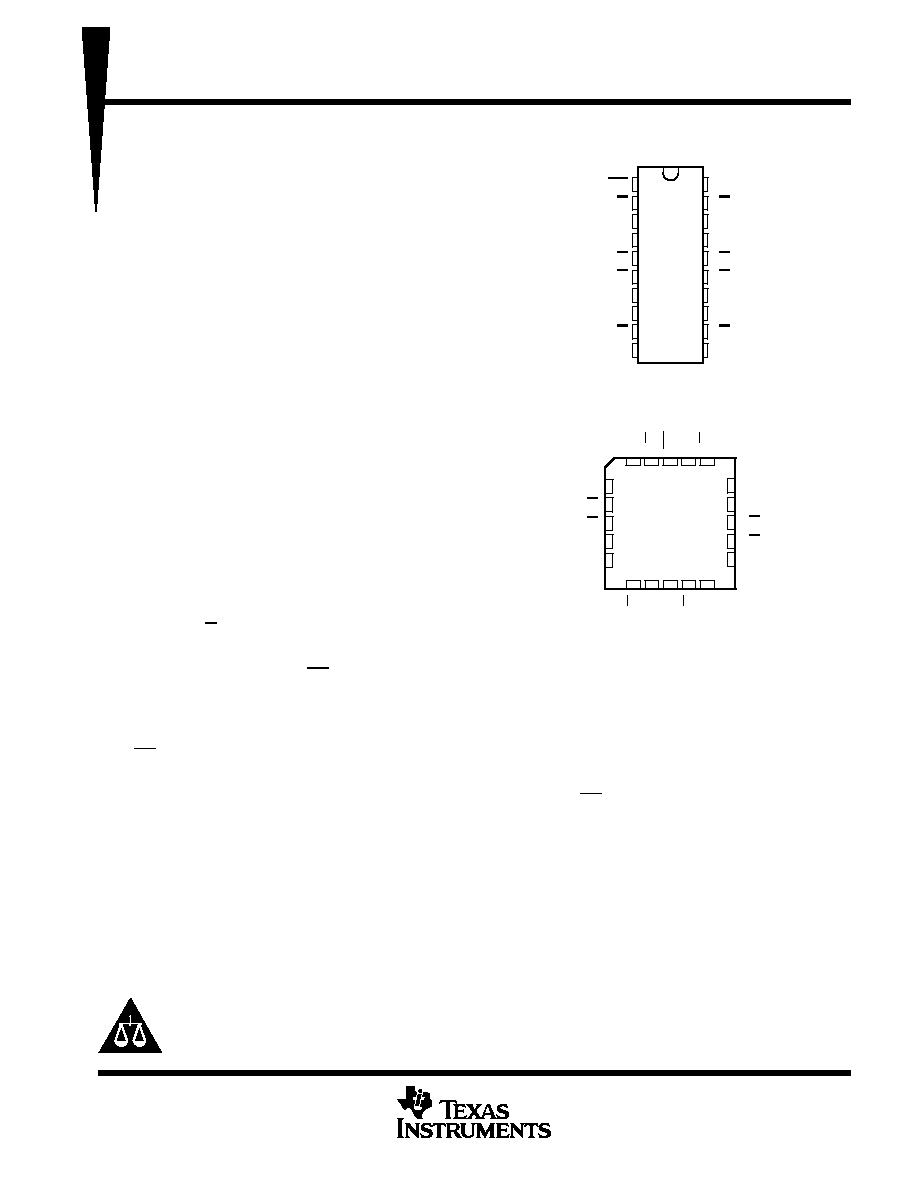
1
2
3
4
5
6
7
8
9
10
20
19
18
17
16
15
14
13
12
11
OE
1Q
1D
2D
2Q
3Q
3D
4D
4Q
GND
V
CC
8Q
8D
7D
7Q
6Q
6D
5D
5Q
CLK
SN54ABT534 . . . J OR W PACKAGE
SN74ABT534A . . . DB, DW, N, OR PW PACKAGE
(TOP VIEW)
3
2 1 20 19
9 10 11 12 13
4
5
6
7
8
18
17
16
15
14
8D
7D
7Q
6Q
6D
2D
2Q
3Q
3D
4D
SN54ABT534 . . . FK PACKAGE
(TOP VIEW)
1D
1Q
OE
5Q
5D
8Q
4Q
GND
CLK
V
CC
SN54ABT534, SN74ABT534A
OCTAL EDGE-TRIGGERED D-TYPE FLIP-FLOPS
WITH 3-STATE OUTPUTS
SCBS187F ≠ JANUARY 1991 ≠ REVISED JANUARY 1997
2
POST OFFICE BOX 655303
∑
DALLAS, TEXAS 75265
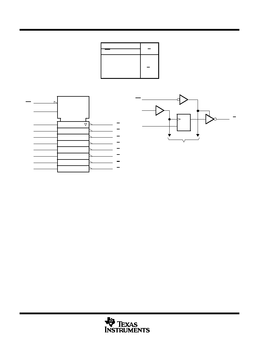
FUNCTION TABLE
(each flip-flop)
INPUTS
OUTPUT
OE
CLK
D
Q
L
H
L
L
L
H
L
H or L
X
Q0
H
X
X
Z
logic symbol
This symbol is in accordance with ANSI/IEEE Std 91-1984 and
IEC Publication 617-12.
1D
3
1D
4
2D
7
3D
8
4D
13
5D
14
6D
17
7D
18
8D
2
5
6
9
12
15
16
19
EN
1
C1
11
CLK
OE
1Q
2Q
3Q
4Q
5Q
6Q
8Q
7Q
logic diagram (positive logic)
1D
C1
OE
1D
1Q
CLK
1
11
3
2
To Seven Other Channels
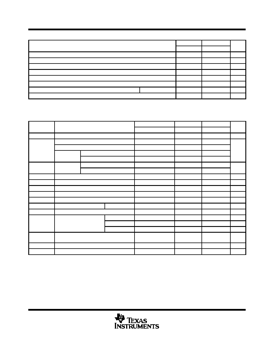
absolute maximum ratings over operating free-air temperature range (unless otherwise noted)
Supply voltage range, V
CC
≠0.5 V to 7 V
. . . . . . . . . . . . . . . . . . . . . . . . . . . . . . . . . . . . . . . . . . . . . . . . . . . . . . . . . .
Input voltage range, V
I
(see Note 1)
≠0.5 V to 7 V
. . . . . . . . . . . . . . . . . . . . . . . . . . . . . . . . . . . . . . . . . . . . . . . . . .
Voltage range applied to any output in the high or power-off state, V
O
≠0.5 V to 5.5 V
. . . . . . . . . . . . . . . . . . .
Current into any output in the low state, I
O
: SN54ABT534 96
mA
. . . . . . . . . . . . . . . . . . . . . . . . . . . . . . . . . . . .
SN74ABT534A 128
mA
. . . . . . . . . . . . . . . . . . . . . . . . . . . . . . . . . .
Input clamp current, I
IK
(V
I
< 0)
≠18 mA
. . . . . . . . . . . . . . . . . . . . . . . . . . . . . . . . . . . . . . . . . . . . . . . . . . . . . . . . . . .
Output clamp current, I
OK
(V
O
< 0)
≠50 mA
. . . . . . . . . . . . . . . . . . . . . . . . . . . . . . . . . . . . . . . . . . . . . . . . . . . . . . . .
Package thermal impedance,
JA
(see Note 2): DB package
115
∞
C/W
. . . . . . . . . . . . . . . . . . . . . . . . . . . . . . . .
DW package
97
∞
C/W
. . . . . . . . . . . . . . . . . . . . . . . . . . . . . . . . .
N package
67
∞
C/W
. . . . . . . . . . . . . . . . . . . . . . . . . . . . . . . . . . .
PW package
128
∞
C/W
. . . . . . . . . . . . . . . . . . . . . . . . . . . . . . . .
Storage temperature range, T
stg
≠65
∞
C to 150
∞
C
. . . . . . . . . . . . . . . . . . . . . . . . . . . . . . . . . . . . . . . . . . . . . . . . . . .
Stresses beyond those listed under "absolute maximum ratings" may cause permanent damage to the device. These are stress ratings only, and
functional operation of the device at these or any other conditions beyond those indicated under "recommended operating conditions" is not
implied. Exposure to absolute-maximum-rated conditions for extended periods may affect device reliability.
NOTES:
1. The input and output negative-voltage ratings may be exceeded if the input and output clamp-current ratings are observed.
2. The package thermal impedance is calculated in accordance with EIA/JEDEC Std JESD51, except for through-hole packages,
which use a trace length of zero.
SN54ABT534, SN74ABT534A
OCTAL EDGE-TRIGGERED D-TYPE FLIP-FLOPS
WITH 3-STATE OUTPUTS
SCBS187F ≠ JANUARY 1991 ≠ REVISED JANUARY 1997
3
POST OFFICE BOX 655303
∑
DALLAS, TEXAS 75265
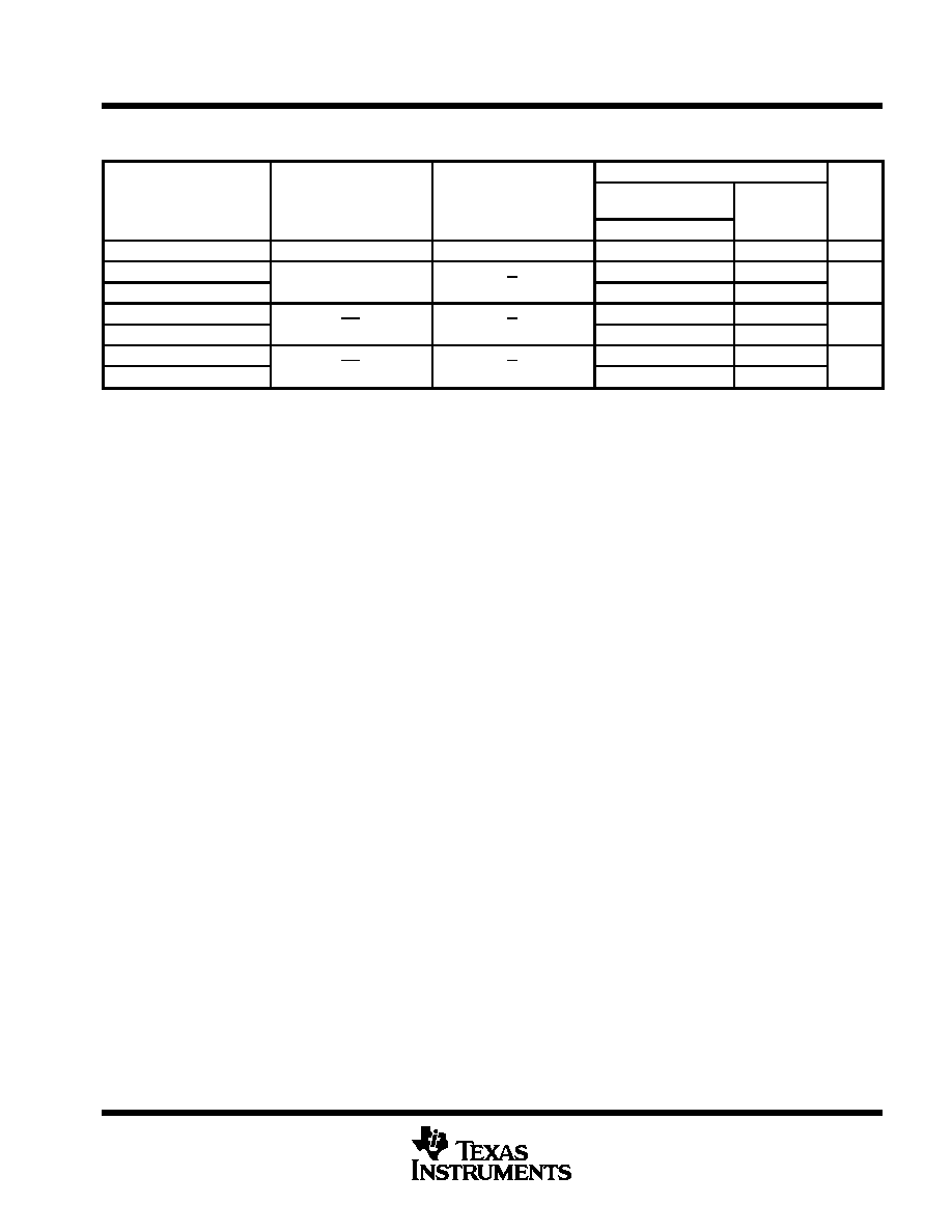
recommended operating conditions (see Note 3)
SN54ABT534
SN74ABT534A
UNIT
MAX
MIN
MAX
UNIT
VCC
Supply voltage
4.5
5.5
4.5
5.5
V
VIH
High-level input voltage
2
2
V
VIL
Low-level input voltage
0.8
0.8
V
VI
Input voltage
0
VCC
0
VCC
V
IOH
High-level output current
≠24
≠32
mA
IOL
Low-level output current
48
64
mA
t/
v
Input transition rise or fall rate
Outputs enabled
5
5
ns/V
TA
Operating free-air temperature
≠55
125
≠40
85
∞
C
NOTE 3: Unused inputs must be held high or low to prevent them from floating.
electrical characteristics over recommended operating free-air temperature range (unless
otherwise noted)
PARAMETER
TEST CONDITIONS
TA = 25
∞
C
SN54ABT534
SN74ABT534A
UNIT
PARAMETER
TEST CONDITIONS
MIN
TYP
MAX
MIN
MAX
MIN
MAX
UNIT
VIK
VCC = 4.5 V,
II = ≠18 mA
≠1.2
≠1.2
≠1.2
V
VCC = 4.5 V,
IOH = ≠3 mA
2.5
2.5
2.5
VOH
VCC = 5 V,
IOH = ≠3 mA
3
3
3
V
VOH
VCC = 4 5 V
IOH = ≠24 mA
2
2
V
VCC = 4.5 V
IOH = ≠32 mA
2*
2
VOL
VCC = 4 5 V
IOL = 48 mA
0.55
0.55
V
VOL
VCC = 4.5 V
IOL = 64 mA
0.55*
0.55
V
Vhys
100
mV
II
VCC = 5.5 V,
VI = VCC or GND
±
1
±
1
±
1
µ
A
IOZH
VCC = 5.5 V,
VO = 2.7 V
10
10
10
µ
A
IOZL
VCC = 5.5 V,
VO = 0.5 V
≠10
≠10
≠10
µ
A
Ioff
VCC = 0,
VI or VO
4.5 V
±
100
±
100
µ
A
ICEX
VCC = 5.5 V,
VO = 5.5 V
Outputs high
50
50
50
µ
A
IOß
VCC = 5.5 V,
VO = 2.5 V
≠50
≠100
≠180
≠50
≠180
≠50
≠180
mA
V
5 5 V I
0
Outputs high
1
250
250
250
µ
A
ICC
VCC = 5.5 V, IO = 0,
VI = VCC or GND
Outputs low
24
30
30
30
mA
VI = VCC or GND
Outputs disabled
0.5
250
250
250
µ
A
ICC∂
VCC = 5.5 V, One input at 3.4 V,
Other inputs at VCC or GND
1.5
1.5
1.5
mA
Ci
VI = 2.5 V or 0.5 V
3.5
pF
Co
VO = 2.5 V or 0.5 V
6.5
pF
* On products compliant to MIL-PRF-38535, this parameter does not apply.
All typical values are at VCC = 5 V.
This data sheet limit may vary among suppliers.
ß Not more than one output should be tested at a time, and the duration of the test should not exceed one second.
∂ This is the increase in supply current for each input that is at the specified TTL voltage level rather than VCC or GND.
SN54ABT534, SN74ABT534A
OCTAL EDGE-TRIGGERED D-TYPE FLIP-FLOPS
WITH 3-STATE OUTPUTS
SCBS187F ≠ JANUARY 1991 ≠ REVISED JANUARY 1997
4
POST OFFICE BOX 655303
∑
DALLAS, TEXAS 75265
timing requirements over recommended ranges of supply voltage and operating free-air
temperature (unless otherwise noted) (see Figure 1)
SN54ABT534
VCC = 5 V,
TA = 25
∞
C
MIN
MAX
UNIT
MIN
MAX
fclock
Clock frequency
125
125
MHz
tw
Pulse duration
CLK high or low
3.5
3.5
ns
tsu
Setup time, data before CLK
High or low
1.6
1.6
ns
th
Hold time, data after CLK
High or low
1.6
1.6
ns
timing requirements over recommended ranges of supply voltage and operating free-air
temperature (unless otherwise noted) (see Figure 1)
SN74ABT534A
VCC = 5 V,
TA = 25
∞
C
MIN
MAX
UNIT
MIN
MAX
fclock
Clock frequency
125
125
MHz
tw
Pulse duration
CLK high or low
3.5
3.5
ns
tsu
Setup time, data before CLK
High or low
1.6
1.6
ns
th
Hold time, data after CLK
High or low
2
2
ns
This data sheet limit may vary among suppliers.
switching characteristics over recommended ranges of supply voltage and operating free-air
temperature, C
L
= 50 pF (unless otherwise noted) (see Figure 1)
SN54ABT534
PARAMETER
FROM
(INPUT)
TO
(OUTPUT)
VCC = 5 V,
TA = 25
∞
C
MIN
MAX
UNIT
MIN
TYP
MAX
fmax
125
175
125
MHz
tPLH
CLK
Q
2.6
4.5
6.1
2.6
7
ns
tPHL
CLK
Q
3.4
5.5
6.7
3.4
7.9
ns
tPZH
OE
Q
1
3.4
5.2
1
5.8
ns
tPZL
OE
Q
2.6
4
5.8
2.6
7
ns
tPHZ
OE
Q
2.4
4.7
6.6
2.4
7.6
ns
tPLZ
OE
Q
2.3
3.8
5.8
2.3
6.8
ns
SN54ABT534, SN74ABT534A
OCTAL EDGE-TRIGGERED D-TYPE FLIP-FLOPS
WITH 3-STATE OUTPUTS
SCBS187F ≠ JANUARY 1991 ≠ REVISED JANUARY 1997
5
POST OFFICE BOX 655303
∑
DALLAS, TEXAS 75265
switching characteristics over recommended ranges of supply voltage and operating free-air
temperature, C
L
= 50 pF (unless otherwise noted) (see Figure 1)
SN74ABT534A
PARAMETER
FROM
(INPUT)
TO
(OUTPUT)
VCC = 5 V,
TA = 25
∞
C
MIN
MAX
UNIT
MIN
TYP
MAX
fmax
125
175
125
MHz
tPLH
CLK
Q
2.6
4.5
5.9
2.6
6.7
ns
tPHL
CLK
Q
3.4
5.5
6.7
3.4
7.6
ns
tPZH
OE
Q
1
3.4
4.2
1
5
ns
tPZL
OE
Q
2.6
4
5.8
2.6
6.8
ns
tPHZ
OE
Q
2.4
4.7
6.6
2.4
7.3
ns
tPLZ
OE
Q
2.3
3.8
5.8
2.3
6.5
ns