SN54ABT7820
512
◊
18
◊
2
STROBED BIDIRECTIONAL FIRST-IN, FIRST-OUT MEMORY
SGBS303E ≠ AUGUST 1994 ≠ REVISED APRIL 2000
1
POST OFFICE BOX 655303
∑
DALLAS, TEXAS 75265
D
Member of the Texas Instruments
Widebus
TM
Family
D
Advanced BiCMOS Technology
D
Released as DSCC SMD (Standard
Microcircuit Drawing) 5962-9650901QXA
D
Independent Asynchronous Inputs and
Outputs
D
Two Separate 512
◊
18 FIFOs Buffering
Data in Opposite Directions
D
Programmable Almost-Full/Almost-Empty
Flag
D
Empty, Full, and Half-Full Flags
D
Fast Access Times of 12 ns With a 50-pF
Load and Simultaneous Switching Data
Outputs
D
Packaged in 84-Pin Ceramic Pin Grid
Array
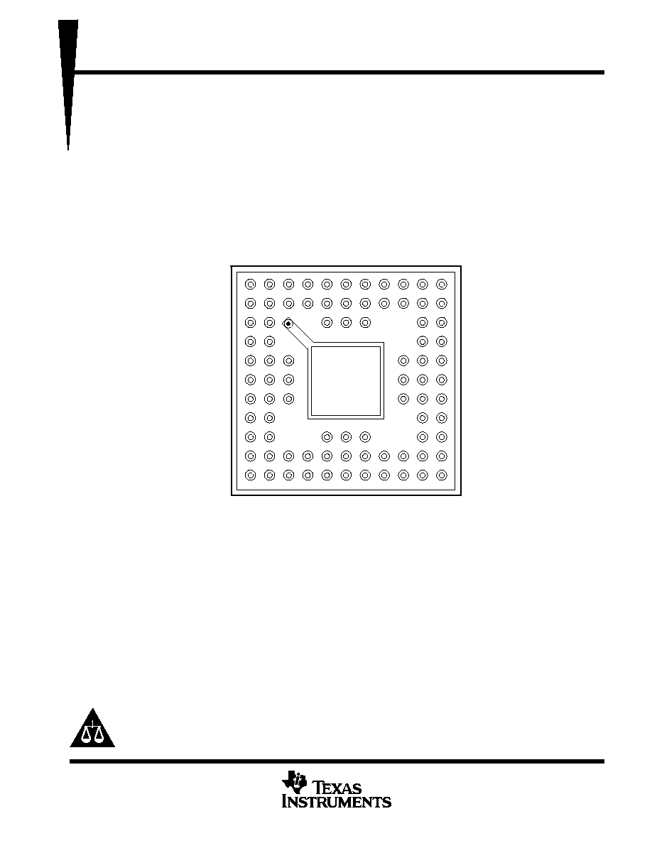
GB PACKAGE
(TOP VIEW)
A
B
C
D
E
F
G
H
J
K
L
1
2
3
4
5
6
7
8
9
10 11
description
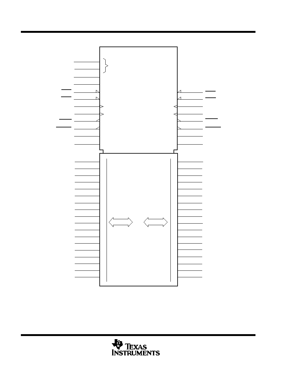
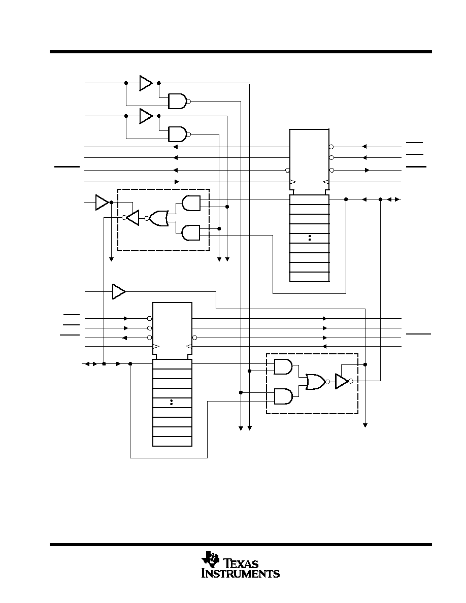
A FIFO memory is a storage device that allows data to be written into and read from its array at independent
data rates. The SN54ABT7820 is arranged as two 512
◊
18-bit FIFOs for high speed and fast access times.
It processes data at rates up to 40 MHz, with access times of 18 ns in a bit-parallel format.
The SN54ABT7820 consists of bus transceiver circuits, two 512
◊
18 FIFOs, and control circuitry arranged for
multiplexed transmission of data directly from the data bus or from the internal FIFO memories. Enable inputs
GAB and GBA control the transceiver functions. The SAB and SBA control inputs select whether real-time or
stored data is transferred. The circuitry used for select control eliminates the typical decoding glitch that occurs
in a multiplexer during the transition between stored and real-time data. Figure 1 illustrates the eight
fundamental bus-management functions that can be performed with the SN54ABT7820.
The SN54ABT7820 is characterized for operation over the full military temperature range of ≠55
∞
C to 125
∞
C.
Copyright
©
1998, Texas Instruments Incorporated
PRODUCTION DATA information is current as of publication date.
Products conform to specifications per the terms of Texas Instruments
standard warranty. Production processing does not necessarily include
testing of all parameters.
Widebus is a trademark of Texas Instruments.
Please be aware that an important notice concerning availability, standard warranty, and use in critical applications of
Texas Instruments semiconductor products and disclaimers thereto appears at the end of this data sheet.
On products compliant to MIL-PRF-38535, all parameters are tested
unless otherwise noted. On all other products, production
processing does not necessarily include testing of all parameters.
SN54ABT7820
512
◊
18
◊
2
STROBED BIDIRECTIONAL FIRST-IN, FIRST-OUT MEMORY
SGBS303E ≠ AUGUST 1994 ≠ REVISED APRIL 2000
3
POST OFFICE BOX 655303
∑
DALLAS, TEXAS 75265
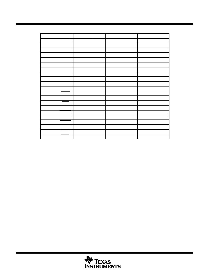
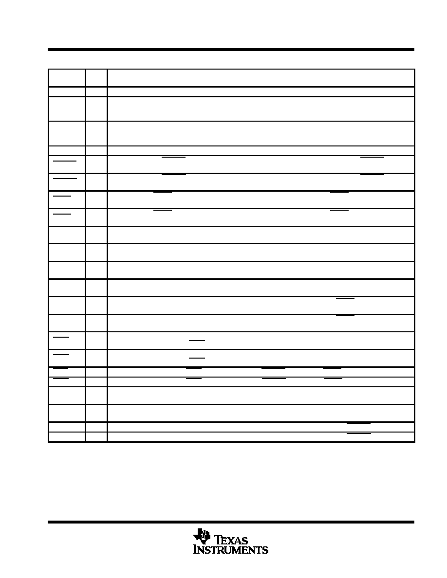
Terminal Functions
TERMINAL
NAME
I/O
DESCRIPTION
A0 ≠ A17
I/O
Port-A data. The 18-bit bidirectional data port for side A.
AF/AEA
O
FIFO A almost-full/almost-empty flag. Depth offset values can be programmed for AF/AEA, or the default value of 128
can be used for both the almost-empty offset (X) and the almost-full offset (Y). AF/AEA is high when FIFO A contains
X or fewer words or (512 ≠ Y) or more words. AF/AEA is set high after FIFO A is reset.
AF/AEB
O
FIFO B almost-full/almost-empty flag. Depth offset values can be programmed for AF/AEB, or the default value of 128
can be used for both the almost-empty offset (X) and the almost-full offset (Y). AF/AEB is high when FIFO B contains
X or fewer words or (512 ≠ Y) or more words. AF/AEB is set high after FIFO B is reset.
B0 ≠ B17
I/O
Port-B data. The 18-bit bidirectional data port for side B.
EMPTYA
O
FIFO A empty flag. EMPTYA is low when FIFO A is empty and is high when FIFO A is not empty. EMPTYA is set low
after FIFO A is reset.
EMPTYB
O
FIFO B empty flag. EMPTYB is low when FIFO B is empty and is high when FIFO B is not empty. EMPTYB is set low
after FIFO B is reset.
FULLA
O
FIFO A full flag. FULLA is low when FIFO A is full and is high when FIFO A is not full. FULLA is set high after FIFO A
is reset.
FULLB
O
FIFO B full flag. FULLB is low when FIFO B is full and is high when FIFO B is not full. FULLB is set high after FIFO B
is reset.
GAB
I
Port-B output enable. B0 ≠ B17 outputs are active when GAB is high and are in the high-impedance state when GAB
is low.
GBA
I
Port-A output enable. A0 ≠ A17 outputs are active when GBA is high and are in the high-impedance state when GBA
is low.
HFA
O
FIFO A half-full flag. HFA is high when FIFO A contains 256 or more words and is low when FIFO A contains 255 or
fewer words. HFA is set low after FIFO A is reset.
HFB
O
FIFO B half-full flag. HFB is high when FIFO B contains 256 or more words and is low when FIFO B contains 255 or
fewer words. HFB is set low after FIFO B is reset.
LDCKA
I
FIFO A load clock. Data is written into FIFO A on a low-to-high transition of LDCKA when FULLA is high. The first word
written into an empty FIFO A is sent directly to the FIFO A data outputs.
LDCKB
I
FIFO B load clock. Data is written into FIFO B on a low-to-high transition of LDCKB when FULLB is high. The first word
written into an empty FIFO B is sent directly to the FIFO B data outputs.
PENA
I
FIFO A program enable. After reset and before a word is written into FIFO A, the binary value on A0 ≠ A7 is latched as
an AF/AEA offset value when PENA is low and LDCKA is high.
PENB
I
FIFO B program enable. After reset and before a word is written into FIFO B, the binary value on B0 ≠ B7 is latched as
an AF/AEB offset value when PENB is low and LDCKB is high.
RSTA
I
FIFO A reset. A low level on RSTA resets FIFO A, forcing EMPTYA low, HFA low, FULLA high, and AF/AEA high.
RSTB
I
FIFO B reset. A low level on RSTB resets FIFO B, forcing EMPTYB low, HFB low, FULLB high, and AF/AEB high.
SAB
I
Port-B read select. SAB selects the source of B0 ≠ B17 read data. A low level selects real-time data from A0 ≠ A17. A
high level selects the FIFO A output.
SBA
I
Port-A read select. SBA selects the source of A0 ≠ A17 read data. A low level selects real-time data from B0 ≠ B17. A
high level selects the FIFO B output.
UNCKA
I
FIFO A unload clock. Data is read from FIFO A on a low-to-high transition of UNCKA when EMPTYA is high.
UNCKB
I
FIFO B unload clock. Data is read from FIFO B on a low-to-high transition of UNCKB when EMPTYB is high.