SN54LVTH16501, SN74LVTH16501
3.3-V ABT 18-BIT UNIVERSAL BUS TRANSCEIVERS
WITH 3-STATE OUTPUTS
SCBS700E ≠ JULY 1997 ≠ REVISED NOVEMBER 2002
1
POST OFFICE BOX 655303
∑
DALLAS, TEXAS 75265
D
Members of the Texas Instruments
Widebus
Family
D
UBT
Transceiver Combines D-Type
Latches and D-Type Flip-Flops for
Operation in Transparent, Latched, or
Clocked Mode
D
State-of-the-Art Advanced BiCMOS
Technology (ABT) Design for 3.3-V
Operation and Low Static-Power
Dissipation
D
Support Mixed-Mode Signal Operation (5-V
Input and Output Voltages With 3.3-V V
CC
)
D
Support Unregulated Battery Operation
Down to 2.7 V
D
Typical V
OLP
(Output Ground Bounce)
<0.8 V at V
CC
= 3.3 V, T
A
= 25
∞
C
D
I
off
and Power-Up 3-State Support Hot
Insertion
D
Bus Hold on Data Inputs Eliminates the
Need for External Pullup/Pulldown
Resistors
D
Distributed V
CC
and GND Pins Minimize
High-Speed Switching Noise
D
Flow-Through Architecture Optimizes PCB
Layout
D
Latch-Up Performance Exceeds 500 mA Per
JESD 17
D
ESD Protection Exceeds JESD 22
≠ 2000-V Human-Body Model (A114-A)
≠ 200-V Machine Model (A115-A)
description/ordering information
The 'LVTH16501 devices are 18-bit universal bus transceivers designed for low-voltage (3.3-V) V
CC
operation,
but with the capability to provide a TTL interface to a 5-V system environment.
ORDERING INFORMATION
TA
PACKAGE
ORDERABLE
PART NUMBER
TOP-SIDE
MARKING
SSOP
DL
Tube
SN74LVTH16501DL
LVTH16501
≠40
∞
C to 85
∞
C
SSOP ≠ DL
Tape and reel
SN74LVTH16501DLR
LVTH16501
TSSOP ≠ DGG
Tape and reel
SN74LVTH16501DGGR
LVTH16501
≠55
∞
C to 125
∞
C
CFP ≠ WD
Tube
SNJ54LVTH16501WD
SNJ54LVTH16501WD
Package drawings, standard packing quantities, thermal data, symbolization, and PCB design guidelines are available
at www.ti.com/sc/package.
Copyright
2002, Texas Instruments Incorporated
Please be aware that an important notice concerning availability, standard warranty, and use in critical applications of
Texas Instruments semiconductor products and disclaimers thereto appears at the end of this data sheet.
Widebus and UBT are trademarks of Texas Instruments.
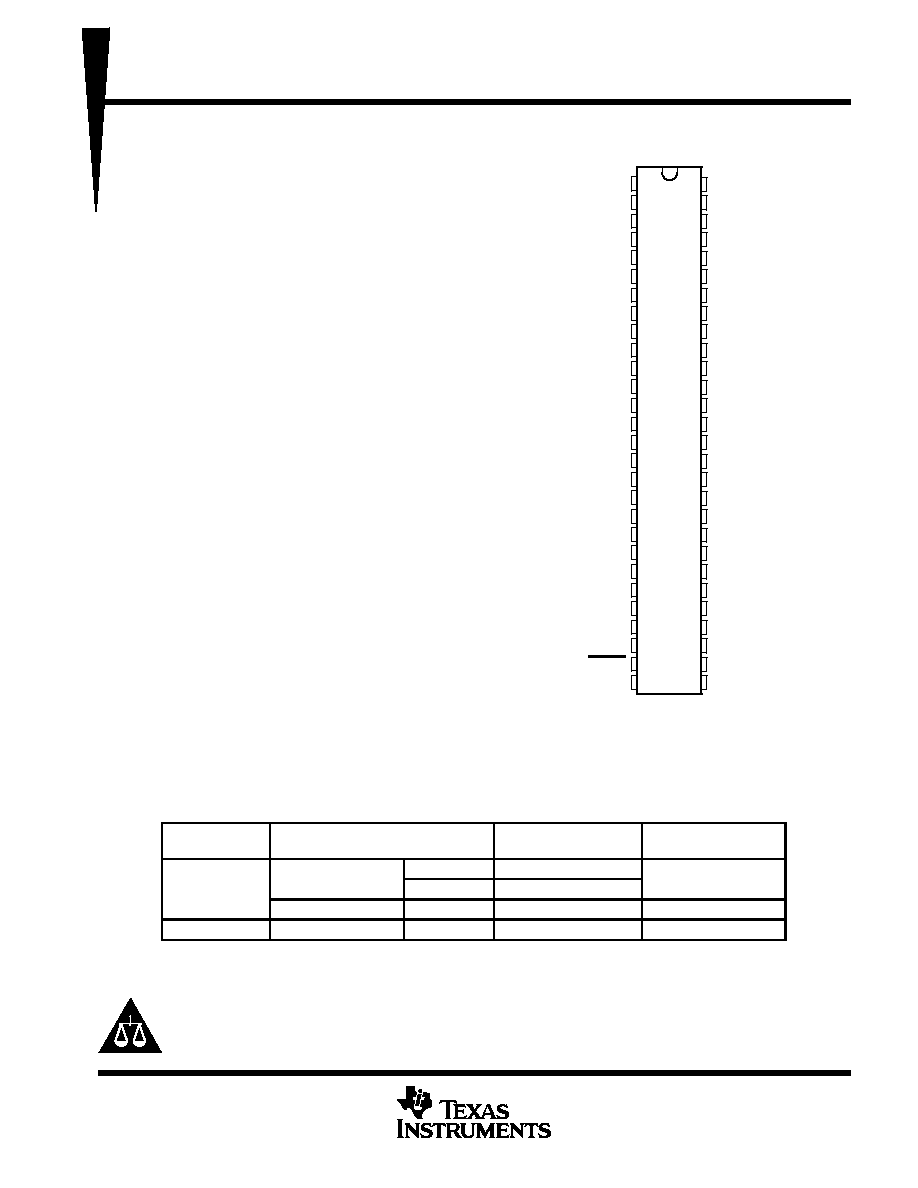
SN54LVTH16501 . . . WD PACKAGE
SN74LVTH16501 . . . DGG OR DL PACKAGE
(TOP VIEW)
1
2
3
4
5
6
7
8
9
10
11
12
13
14
15
16
17
18
19
20
21
22
23
24
25
26
27
28
56
55
54
53
52
51
50
49
48
47
46
45
44
43
42
41
40
39
38
37
36
35
34
33
32
31
30
29
OEAB
LEAB
A1
GND
A2
A3
V
CC
A4
A5
A6
GND
A7
A8
A9
A10
A11
A12
GND
A13
A14
A15
V
CC
A16
A17
GND
A18
OEBA
LEBA
GND
CLKAB
B1
GND
B2
B3
V
CC
B4
B5
B6
GND
B7
B8
B9
B10
B11
B12
GND
B13
B14
B15
V
CC
B16
B17
GND
B18
CLKBA
GND
PRODUCTION DATA information is current as of publication date.
Products conform to specifications per the terms of Texas Instruments
standard warranty. Production processing does not necessarily include
testing of all parameters.
On products compliant to MIL-PRF-38535, all parameters are tested
unless otherwise noted. On all other products, production
processing does not necessarily include testing of all parameters.
SN54LVTH16501, SN74LVTH16501
3.3-V ABT 18-BIT UNIVERSAL BUS TRANSCEIVERS
WITH 3-STATE OUTPUTS
SCBS700E ≠ JULY 1997 ≠ REVISED NOVEMBER 2002
2
POST OFFICE BOX 655303
∑
DALLAS, TEXAS 75265
description/ordering information (continued)
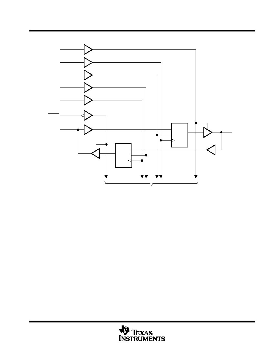
Data flow in each direction is controlled by output-enable (OEAB and OEBA), latch-enable (LEAB and LEBA),
and clock (CLKAB and CLKBA) inputs. For A-to-B data flow, the devices operate in the transparent mode when
LEAB is high. When LEAB is low, the A data is latched if CLKAB is held at a high or low logic level. If LEAB is
low, the A data is stored in the latch/flip-flop on the low-to-high transition of CLKAB. When OEAB is high, the
outputs are active. When OEAB is low, the outputs are in the high-impedance state.
Data flow for B to A is similar to that of A to B but uses OEBA, LEBA, and CLKBA. The output enables are
complementary (OEAB is active high and OEBA is active low).
Active bus-hold circuitry holds unused or undriven inputs at a valid logic state. Use of pullup or pulldown resistors
with the bus-hold circuitry is not recommended.
When V
CC
is between 0 and 1.5 V, the devices are in the high-impedance state during power up or power down.
However, to ensure the high-impedance state above 1.5 V, OE should be tied to V
CC
through a pullup resistor
and OE should be tied to GND through a pulldown resistor; the minimum value of the resistor is determined by
the current-sinking/current-sourcing capability of the driver.
These devices are fully specified for hot-insertion applications using I
off
and power-up 3-state. The I
off
circuitry
disables the outputs, preventing damaging current backflow through the devices when they are powered down.
The power-up 3-state circuitry places the outputs in the high-impedance state during power up and power down,
which prevents driver conflict.
FUNCTION TABLE
INPUTS
OUTPUT
OEAB
LEAB
CLKAB
A
B
L
X
X
X
Z
H
H
X
L
L
H
H
X
H
H
H
L
L
L
H
L
H
H
H
L
H
X
B0
H
L
L
X
B0ß
A-to-B data flow is shown; B-to-A flow is similar, but
uses OEBA, LEBA, and CLKBA.
Output level before the indicated steady-state input
conditions were established, provided that CLKAB
was high before LEAB went low
ß Output level before the indicated steady-state input
conditions were established
SN54LVTH16501, SN74LVTH16501
3.3-V ABT 18-BIT UNIVERSAL BUS TRANSCEIVERS
WITH 3-STATE OUTPUTS
SCBS700E ≠ JULY 1997 ≠ REVISED NOVEMBER 2002
3
POST OFFICE BOX 655303
∑
DALLAS, TEXAS 75265
logic diagram (positive logic)
1D
C1
CLK
1D
C1
CLK
B1
OEAB
CLKAB
LEAB
LEBA
CLKBA
OEBA
A1
1
55
2
28
30
27
3
54
To 17 Other Channels
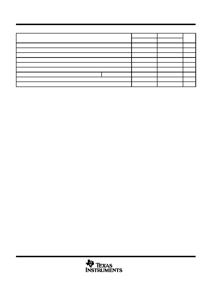
absolute maximum ratings over operating free-air temperature range (unless otherwise noted)
Supply voltage range, V
CC
≠0.5 V to 4.6 V
. . . . . . . . . . . . . . . . . . . . . . . . . . . . . . . . . . . . . . . . . . . . . . . . . . . . . . . . .
Input voltage range, V
I
(see Note 1)
≠0.5 V to 7 V
. . . . . . . . . . . . . . . . . . . . . . . . . . . . . . . . . . . . . . . . . . . . . . . . . .
Voltage range applied to any output in the high-impedance
or power-off state, V
O
(see Note 1)
≠0.5 V to 7 V
. . . . . . . . . . . . . . . . . . . . . . . . . . . . . . . . . . . . . . . . . . . . . . . .
Voltage range applied to any output in the high state, V
O
(see Note 1)
≠0.5 V to V
CC
+ 0.5 V
. . . . . . . . . . . . .
Current into any output in the low state, I
O
: SN54LVTH16501 96
mA
. . . . . . . . . . . . . . . . . . . . . . . . . . . . . . . . .
SN74LVTH16501 128
mA
. . . . . . . . . . . . . . . . . . . . . . . . . . . . . . . .
Current into any output in the high state, I
O
(see Note 2): SN54LVTH16501
48 mA
. . . . . . . . . . . . . . . . . . . . .
SN74LVTH16501 64
mA
. . . . . . . . . . . . . . . . . . . . .
Input clamp current, I
IK
(V
I
< 0)
≠50 mA
. . . . . . . . . . . . . . . . . . . . . . . . . . . . . . . . . . . . . . . . . . . . . . . . . . . . . . . . . . .
Output clamp current, I
OK
(V
O
< 0)
≠50 mA
. . . . . . . . . . . . . . . . . . . . . . . . . . . . . . . . . . . . . . . . . . . . . . . . . . . . . . . .
Package thermal impedance,
JA
(see Note 3): DGG package
64
∞
C/W
. . . . . . . . . . . . . . . . . . . . . . . . . . . . . . .
DL package
56
∞
C/W
. . . . . . . . . . . . . . . . . . . . . . . . . . . . . . . . .
Storage temperature range, T
stg
≠65
∞
C to 150
∞
C
. . . . . . . . . . . . . . . . . . . . . . . . . . . . . . . . . . . . . . . . . . . . . . . . . . .
Stresses beyond those listed under "absolute maximum ratings" may cause permanent damage to the device. These are stress ratings only, and
functional operation of the device at these or any other conditions beyond those indicated under "recommended operating conditions" is not
implied. Exposure to absolute-maximum-rated conditions for extended periods may affect device reliability.
NOTES:
1. The input and output negative-voltage ratings may be exceeded if the input and output clamp-current ratings are observed.
2. This current flows only when the output is in the high state and VO > VCC.
3. The package thermal impedance is calculated in accordance with JESD 51-7.
SN54LVTH16501, SN74LVTH16501
3.3-V ABT 18-BIT UNIVERSAL BUS TRANSCEIVERS
WITH 3-STATE OUTPUTS
SCBS700E ≠ JULY 1997 ≠ REVISED NOVEMBER 2002
4
POST OFFICE BOX 655303
∑
DALLAS, TEXAS 75265
recommended operating conditions (see Note 4)
SN54LVTH16501
SN74LVTH16501
UNIT
MIN
MAX
MIN
MAX
UNIT
VCC
Supply voltage
2.7
3.6
2.7
3.6
V
VIH
High-level input voltage
2
2
V
VIL
Low-level input voltage
0.8
0.8
V
VI
Input voltage
5.5
5.5
V
IOH
High-level output current
≠24
≠32
mA
IOL
Low-level output current
48
64
mA
t/
v
Input transition rise or fall rate
Outputs enabled
10
10
ns/V
t/
VCC
Power-up ramp rate
200
200
µ
s/V
TA
Operating free-air temperature
≠55
125
≠40
85
∞
C
NOTE 4: All unused control inputs of the device must be held at VCC or GND to ensure proper device operation. Refer to the TI application report,
Implications of Slow or Floating CMOS Inputs, literature number SCBA004.
SN54LVTH16501, SN74LVTH16501
3.3-V ABT 18-BIT UNIVERSAL BUS TRANSCEIVERS
WITH 3-STATE OUTPUTS
SCBS700E ≠ JULY 1997 ≠ REVISED NOVEMBER 2002
5
POST OFFICE BOX 655303
∑
DALLAS, TEXAS 75265
electrical characteristics over recommended operating free-air temperature range (unless
otherwise noted)
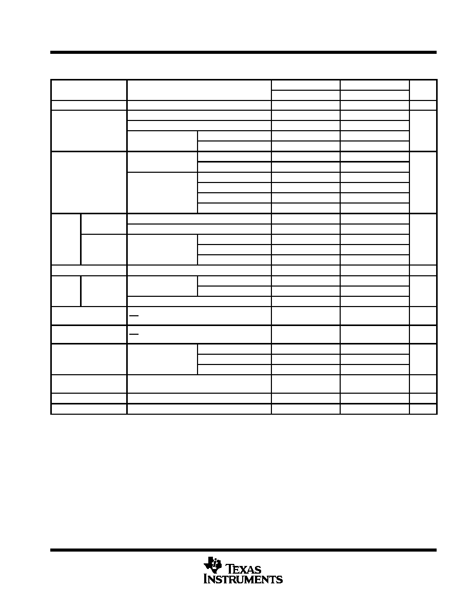
PARAMETER
TEST CONDITIONS
SN54LVTH16501
SN74LVTH16501
UNIT
PARAMETER
TEST CONDITIONS
MIN
TYP
MAX
MIN
TYP
MAX
UNIT
VIK
VCC = 2.7 V,
II = ≠18 mA
≠1.2
≠1.2
V
VCC = 2.7 V to 3.6 V,
IOH = ≠100
µ
A
VCC≠0.2
VCC≠0.2
VOH
VCC = 2.7 V,
IOH = ≠8 mA
2.4
2.4
V
VOH
VCC = 3 V
IOH = ≠24 mA
2
V
VCC = 3 V
IOH = ≠32 mA
2
VCC = 2 7 V
IOL = 100
µ
A
0.2
0.2
VCC = 2.7 V
IOL = 24 mA
0.5
0.5
VOL
IOL = 16 mA
0.4
0.4
V
VOL
VCC = 3 V
IOL = 32 mA
0.5
0.5
V
VCC = 3 V
IOL = 48 mA
0.55
IOL = 64 mA
0.55
Control inputs
VCC = 3.6 V,
VI = VCC or GND
±
1
±
1
Control inputs
VCC = 0 or 3.6 V,
VI = 5.5 V
10
10
II
VI = 5.5 V
20
20
µ
A
A or B ports
VCC = 3.6 V
VI = VCC
1
1
VI = 0
≠5
≠5
Ioff
VCC = 0,
VI or VO = 0 to 4.5 V
±
100
µ
A
VCC = 3 V
VI = 0.8 V
75
75
II(hold)
A or B ports
VCC = 3 V
VI = 2 V
≠75
≠75
µ
A
(
)
VCC = 3.6 Vß,
VI = 0 to 3.6 V
±
500
IOZPU
VCC = 0 to 1.5 V, VO = 0.5 V to 3 V,
OE/OE = don't care
±
100*
±
100
µ
A
IOZPD
VCC = 1.5 V to 0, VO = 0.5 V to 3 V,
OE/OE = don't care
±
100*
±
100
µ
A
VCC = 3.6 V,
Outputs high
0.19
0.19
ICC
VCC = 3.6 V,
IO = 0,
Outputs low
5
5
mA
VI = VCC or GND
Outputs disabled
0.19
0.19
ICC∂
VCC = 3 V to 3.6 V, One input at VCC ≠ 0.6 V,
Other inputs at VCC or GND
0.2
0.2
mA
Ci
VI = 3 V or 0
4
4
pF
Cio
VO = 3 V or 0
10
10
pF
* On products compliant to MIL-PRF-38535, this parameter is not production tested.
All typical values are at VCC = 3.3 V, TA = 25
∞
C.
Unused pins at VCC or GND
ß This is the bus-hold maximum dynamic current. It is the minimum overdrive current required to switch the input from one state to another.
∂ This is the increase in supply current for each input that is at the specified TTL voltage level rather than VCC or GND.