THS4041, THS4042
165-MHz C-STABLE HIGH-SPEED AMPLIFIERS
SLOS237B≠ MAY 1999 ≠ REVISED FEBRUARY 2000
1
POST OFFICE BOX 655303
∑
DALLAS, TEXAS 75265
D
C-Stable Amplifiers Drive Any Capacitive
Load
D
High Speed
≠ 165 MHz Bandwidth (≠3 dB); C
L
= 0 pF
≠ 100 MHz Bandwidth (≠3 dB); C
L
= 100 pF
≠ 35 MHz Bandwidth (≠3 dB); C
L
= 1000 pF
≠ 400 V/
µ
s Slew Rate
D
Unity Gain Stable
D
High Output Drive, I
O
= 100 mA (typ)
D
Very Low Distortion
≠ THD = ≠75 dBc (f = 1 MHz, R
L
= 150
)
≠ THD = ≠89 dBc (f = 1 MHz, R
L
= 1 k
)
D
Wide Range of Power Supplies
≠ V
CC
=
±
5 V to
±
15 V
D
Available in Standard SOIC or MSOP
PowerPAD
TM
Package
D
Evaluation Module Available
description
The THS4041 and THS4042 are single/dual,
high-speed voltage feedback amplifiers capable
of driving any capacitive load. This makes them
ideal for a wide range of applications including
driving video lines or buffering ADCs. The devices
feature high 165-MHz bandwidth and 400-V/
µ
sec
slew rate. The THS4041/2 are stable at all gains
for both inverting and noninverting configurations.
For video applications, the THS4041/2 offer
excellent video performance with 0.01% differen-
tial gain error and 0.01
∞
differential phase error.
These amplifiers can drive up to 100 mA into a
20-
load and operate off power supplies ranging
from
±
5V to
±
15V.
RELATED DEVICES
RELATED DEVICES
DEVICE
DESCRIPTION
THS4011/2
290-MHz Low Distortion High-Speed Amplifier
THS4031/2
100-MHz Low Noise High-Speed Amplifier
THS4081/2
175-MHz Low Power High-Speed Amplifiers
PowerPAD is a trademark of Texas Insruments Incorporated.
Copyright
©
2000, Texas Instruments Incorporated
PRODUCTION DATA information is current as of publication date.
Products conform to specifications per the terms of Texas Instruments
standard warranty. Production processing does not necessarily include
testing of all parameters.
Please be aware that an important notice concerning availability, standard warranty, and use in critical applications of
Texas Instruments semiconductor products and disclaimers thereto appears at the end of this data sheet.
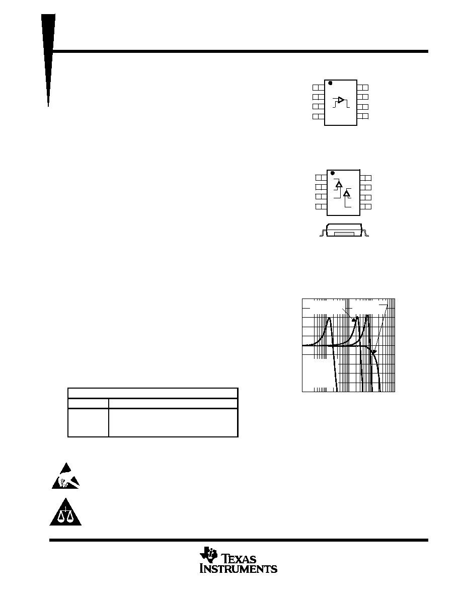
Cross Section View Showing
PowerPAD Option (DGN)
OUTPUT AMPLITUDE
vs
FREQUENCY
f ≠ Frequency ≠ Hz
1G
10M
100k
1M
Output
Amplitude ≠ dB
100M
VCC =
±
15 V
Gain = 1
RF = 200
RL = 150
VO(PP)=62 mV
≠2
≠10
≠6
10
4
2
0
≠8
8
≠4
6
CL = 1000 pF
CL = 0.1
µ
F
CL = 0 pF
CL = 100 pF
1
2
3
4
8
7
6
5
NULL
IN ≠
IN +
V
CC
≠
NULL
V
CC
+
OUT
NC
THS4041
D AND DGN PACKAGE
(TOP VIEW)
NC ≠ No internal connection
1
2
3
4
8
7
6
5
1OUT
1IN ≠
1IN +
V
CC
≠
V
CC
+
2OUT
2IN ≠
2IN+
THS4042
D AND DGN PACKAGE
(TOP VIEW)
CAUTION: The THS4041 and THS4042 provide ESD protection circuitry. However, permanent damage can still occur if this device
is subjected to high-energy electrostatic discharges. Proper ESD precautions are recommended to avoid any performance
degradation or loss of functionality.

THS4041, THS4042
165-MHz C-STABLE HIGH-SPEED AMPLIFIERS
SLOS237B≠ MAY 1999 ≠ REVISED FEBRUARY 2000
2
POST OFFICE BOX 655303
∑
DALLAS, TEXAS 75265
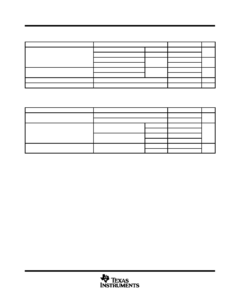
AVAILABLE OPTIONS
PACKAGED DEVICES
TA
NUMBER OF
CHANNELS
PLASTIC
SMALL OUTLINE
(D)
PLASTIC
MSOP
(DGN)
MSOP
SYMBOL
EVALUATION
MODULE
0
∞
C to 70
∞
C
1
THS4041CD
THS4041CDGN
ACO
THS4041EVM
0
∞
C to 70
∞
C
2
THS4042CD
THS4042CDGN
ACC
THS4042EVM
≠ 40
∞
C to 85
∞
C
1
THS4041D
THS4041IDGN
ACP
--
≠ 40
∞
C to 85
∞
C
2
THS4042ID
THS4042IDGN
ACD
--
The D and DGN packages are available taped and reeled. Add an R suffix to the device type (i.e., THS4041CDGNR).
functional block diagram
1OUT
1IN≠
1IN+
VCC
2OUT
2IN≠
2IN+
VCC≠
5
6
1
2
3
8
4
7
Figure 1. THS4042 ≠ Dual Channel
OUT
8
6
1
IN≠
IN+
2
3
Null
Figure 2. THS4041 ≠ Single Channel
absolute maximum ratings over operating free-air temperature (unless otherwise noted)
Supply voltage, V
CC
±
16.5 V
. . . . . . . . . . . . . . . . . . . . . . . . . . . . . . . . . . . . . . . . . . . . . . . . . . . . . . . . . . . . . . . . . . . .
Input voltage, V
I
±
V
CC
. . . . . . . . . . . . . . . . . . . . . . . . . . . . . . . . . . . . . . . . . . . . . . . . . . . . . . . . . . . . . . . . . . . . . . . . . .
Output current, I
O
150 mA
. . . . . . . . . . . . . . . . . . . . . . . . . . . . . . . . . . . . . . . . . . . . . . . . . . . . . . . . . . . . . . . . . . . . . . .
Differential input voltage, V
IO
±
4 V
. . . . . . . . . . . . . . . . . . . . . . . . . . . . . . . . . . . . . . . . . . . . . . . . . . . . . . . . . . . . . . . .
Continuous total power dissipation
See Dissipation Rating Table
. . . . . . . . . . . . . . . . . . . . . . . . . . . . . . . . . . . . .
Maximum junction temperature, T
J
150
∞
C
. . . . . . . . . . . . . . . . . . . . . . . . . . . . . . . . . . . . . . . . . . . . . . . . . . . . . . . .
Operating free-air temperature, T
A
:
C-suffix 0
∞
C to 70
∞
C
. . . . . . . . . . . . . . . . . . . . . . . . . . . . . . . . . . . . . . . . . . .
I-suffix ≠ 40
∞
C to 85
∞
C
. . . . . . . . . . . . . . . . . . . . . . . . . . . . . . . . . . . . . . . . . .
Storage temperature, T
stg
≠ 65
∞
C to 150
∞
C
. . . . . . . . . . . . . . . . . . . . . . . . . . . . . . . . . . . . . . . . . . . . . . . . . . . . . . . . .
Lead temperature 1,6 mm (1/16 inch) from case for 10 seconds
300
∞
C
. . . . . . . . . . . . . . . . . . . . . . . . . . . . . . .
Stresses beyond those listed under "absolute maximum ratings" may cause permanent damage to the device. These are stress ratings only and
functional operation of the device at these or any other conditions beyond those indicated under "recommended operating conditions" is not
implied. Exposure to absolute-maximum-rated conditions for extended periods may affect device reliability.

THS4041, THS4042
165-MHz C-STABLE HIGH-SPEED AMPLIFIERS
SLOS237B≠ MAY 1999 ≠ REVISED FEBRUARY 2000
3
POST OFFICE BOX 655303
∑
DALLAS, TEXAS 75265
DISSIPATION RATING TABLE
PACKAGE
JA
JC
TA = 25
∞
C
PACKAGE
JA
(
∞
C/W)
JC
(
∞
C/W)
A
POWER RATING
D
167
38.3
740 mW
DGN
58.4
4.7
2.14 W
This data was taken using the JEDEC standard Low-K test PCB. For the JEDEC proposed
High-K test PCB, the
JA is 95
∞
C/W with a power rating at TA = 25
∞
C of 1.32 W.
This data was taken using 2 oz. trace and copper pad that is soldered directly to a 3 in.
◊
3 in.
PC. For further information, refer to
Application Information section of this data sheet.
recommended operating conditions
MIN
NOM
MAX
UNIT
Supply voltage VCC and VCC
Dual supply
±
4.5
±
16
V
Supply voltage, VCC+ and VCC≠
Single supply
9
32
V
Operating free air temperature TA
C-suffix
0
70
∞
C
Operating free-air temperature, TA
I-suffix
≠40
85
∞
C
electrical characteristics at T
A
= 25
∞
C, V
CC
=
±
15 V, R
L
= 150
(unless otherwise noted)
dynamic performance
PARAMETER
TEST CONDITIONS
MIN
TYP
MAX
UNIT
VCC =
±
15 V
Rf = 200
Gain = 1
165
MHz
Dynamic performance small-signal bandwidth
VCC =
±
5 V
Rf = 200
Gain = 1
150
MHz
y
g
(≠3 dB)
VCC =
±
15 V
Rf = 1.3 k
Gain = 2
60
MHz
BW
VCC =
±
5 V
Rf = 1.3 k
Gain = 2
60
MHz
BW
Bandwidth for 0 1 dB flatness
VCC =
±
15 V
Rf = 200
Gain = 1
45
MHz
Bandwidth for 0.1 dB flatness
VCC =
±
5 V
Rf = 200
Gain = 1
45
MHz
F ll po er band idthß
VO(pp) = 20 V,
VCC =
±
15 V
6.3
MHz
Full power bandwidthß
VO(pp) = 5 V,
VCC =
±
5 V
20
MHz
SR
Sle
rate
VCC =
±
15 V,
20-V step,
Gain = 5
400
V/
µ
s
SR
Slew rate
VCC =
±
5 V,
5-V step,
Gain = ≠1
325
V/
µ
s
Settling time to 0 1%
VCC =
±
15 V,
5-V step
Gain = 1
120
ns
t
Settling time to 0.1%
VCC =
±
5 V,
2-V step
Gain = ≠1
120
ns
ts
Settling time to 0 01%
VCC =
±
15 V,
5-V step
Gain = 1
250
ns
Settling time to 0.01%
VCC =
±
5 V,
2-V step
Gain = ≠1
280
ns
Full range = 0
∞
C to 70
∞
C for C suffix and ≠ 40
∞
C to 85
∞
C for I suffix
Slew rate is measured from an output level range of 25% to 75%.
ß Full power bandwidth = slew rate / 2
VO(Peak).

THS4041, THS4042
165-MHz C-STABLE HIGH-SPEED AMPLIFIERS
SLOS237B≠ MAY 1999 ≠ REVISED FEBRUARY 2000
4
POST OFFICE BOX 655303
∑
DALLAS, TEXAS 75265
electrical characteristics at T
A
= 25
∞
C, V
CC
=
±
15 V, R
L
= 150
(unless otherwise noted) (continued)
noise/distortion performance
PARAMETER
TEST CONDITIONS
MIN
TYP
MAX
UNIT
VCC =
±
15 V
RL = 150
≠75
THD
Total harmonic distortion
VO(pp) = 2 V,
VCC =
±
15 V
RL = 1 k
≠89
dBc
THD
Total harmonic distortion
O(
)
,
f = 1 MHz, Gain = 2
VCC =
±
5 V
RL = 150
≠75
dBc
VCC =
±
5 V
RL = 1 k
≠86
Vn
Input voltage noise
VCC =
±
5 V or
±
15 V,
f = 10 kHz
14
nV/
Hz
In
Input current noise
VCC =
±
5 V or
±
15 V,
f = 10 kHz
0.9
pA/
Hz
Differential gain error
Gain = 2,
NTSC,
VCC =
±
15 V
0.01%
Differential gain error
,
40 IRE modulation,
,
±
100 IRE ramp
VCC =
±
5 V
0.01%
Differential phase error
Gain = 2,
NTSC,
VCC =
±
15 V
0.01
∞
Differential phase error
,
40 IRE modulation,
,
±
100 IRE ramp
VCC =
±
5 V
0.02
∞
Channel-to-channel crosstalk
(THS4042 only)
VCC =
±
5 V or
±
15 V,
f = 1 MHz
Gain = 2
≠64
dB
Full range = 0
∞
C to 70
∞
C for C suffix and ≠ 40
∞
C to 85
∞
C for I suffix
dc performance
PARAMETER
TEST CONDITIONS
MIN
TYP
MAX
UNIT
VCC =
±
15 V,
VO =
±
10 V,
TA = 25
∞
C
74
80
Open loop gain
CC
,
O
,
RL = 1 k
TA = full range
69
dB
Open loop gain
VCC =
±
5 V,
VO =
±
2.5 V,
TA = 25
∞
C
69
76
dB
CC
,
O
,
RL = 250
TA = full range
66
VOS
Input offset voltage
VCC =
±
5 V or
±
15 V
TA = 25
∞
C
2.5
10
mV
VOS
Input offset voltage
VCC =
±
5 V or
±
15 V
TA = full range
13
mV
Offset voltage drift
VCC =
±
5 V or
±
15 V
TA = full range
10
µ
V/
∞
C
IIB
Input bias current
VCC =
±
5 V or
±
15 V
TA = 25
∞
C
2.5
6
µ
A
IIB
Input bias current
VCC =
±
5 V or
±
15 V
TA = full range
8
µ
A
IOS
Input offset current
VCC =
±
5 V or
±
15 V
TA = 25
∞
C
35
250
nA
IOS
Input offset current
VCC =
±
5 V or
±
15 V
TA = full range
400
nA
Offset current drift
TA = full range
0.3
nA/
∞
C
Full range = 0
∞
C to 70
∞
C for C suffix and ≠ 40
∞
C to 85
∞
C for I suffix
input characteristics
PARAMETER
TEST CONDITIONS
MIN
TYP
MAX
UNIT
VICR
Common mode input voltage range
VCC =
±
15 V
±
13.8
±
14.3
V
VICR
Common-mode input voltage range
VCC =
±
5 V
±
3.8
±
4.3
V
CMRR
Common mode rejection ratio
VCC =
±
15 V,
VICR =
±
12 V
TA = full range
70
90
dB
CMRR
Common mode rejection ratio
VCC =
±
5 V,
VICR =
±
2.5 V
TA = full range
80
100
dB
ri
Input resistance
1
M
Ci
Input capacitance
1.5
pF
Full range = 0
∞
C to 70
∞
C for C suffix and ≠ 40
∞
C to 85
∞
C for I suffix
THS4041, THS4042
165-MHz C-STABLE HIGH-SPEED AMPLIFIERS
SLOS237B≠ MAY 1999 ≠ REVISED FEBRUARY 2000
5
POST OFFICE BOX 655303
∑
DALLAS, TEXAS 75265
electrical characteristics at T
A
= 25
∞
C, V
CC
=
±
15 V, R
L
= 150
(unless otherwise noted) (continued)
output characteristics
PARAMETER
TEST CONDITIONS
MIN
TYP
MAX
UNIT
VCC =
±
15 V
RL = 250
±
11.5
±
13
V
VO
Output voltage swing
VCC =
±
5 V
RL = 150
±
3.2
±
3.5
V
VO
Output voltage swing
VCC =
±
15 V
RL = 1 k
±
13
±
13.6
V
VCC =
±
5 V
RL = 1 k
±
3.5
±
3.8
V
IO
O tp t c rrent
VCC =
±
15 V
RL = 20
80
100
mA
IO
Output current
VCC =
±
5 V
RL = 20
50
65
mA
ISC
Short-circuit current
VCC =
±
15 V
150
mA
RO
Output resistance
Open loop
13
Full range = 0
∞
C to 70
∞
C for C suffix and ≠ 40
∞
C to 85
∞
C for I suffix
Observe power dissipation ratings to keep the junction temperature below the absolute maximum rating when the output is heavily loaded or
shorted. See the absolute maximum ratings section of this data sheet for more information.
power supply
PARAMETER
TEST CONDITIONS
MIN
TYP
MAX
UNIT
VCC
Supply voltage operating range
Dual supply
±
4.5
±
16.5
V
VCC
Supply voltage operating range
Single supply
9
33
V
VCC =
±
15 V
TA = 25
∞
C
8
9.5
ICC
Supply current (per amplifier)
VCC =
±
15 V
TA = full range
11
mA
ICC
Supply current (per amplifier)
VCC =
±
5 V
TA = 25
∞
C
7
8.5
mA
VCC =
±
5 V
TA = full range
10
PSRR
Power supply rejection ratio
VCC =
±
5 V or
±
15 V
TA = 25
∞
C
75
84
dB
PSRR
Power supply rejection ratio
VCC =
±
5 V or
±
15 V
TA = full range
70
dB
Full range = 0
∞
C to 70
∞
C for C suffix and ≠ 40
∞
C to 85
∞
C for I suffix