 | –≠–ª–µ–∫—Ç—Ä–æ–Ω–Ω—ã–π –∫–æ–º–ø–æ–Ω–µ–Ω—Ç: THS4121 | –°–∫–∞—á–∞—Ç—å:  PDF PDF  ZIP ZIP |

www.ti.com
FEATURES
KEY APPLICATIONS
THS4121
D, DGN, OR DGK PACKAGE
(TOP VIEW)
1
2
3
4
8
7
6
5
V
IN-
V
OCM
V
DD
V
OUT+
V
IN+
NC
GND
V
OUT-
THS4120
D, DGN, OR DGK PACKAGE
(TOP VIEW)
1
2
3
4
8
7
6
5
V
IN-
V
OCM
V
DD
V
OUT+
V
IN+
PD
GND
V
OUT-
DESCRIPTION
+
DIGITAL
OUTPUT
V
IN
-
+
-
DV
DD
V
OCM
AV
SS
AV
DD
A
IN
A
IN
V
DD
V
ref
3.3 V
TYPICAL A/D APPLICATION CIRCUIT
THS4120
THS4121
SLOS319D ≠ FEBRUARY 2001 ≠ REVISED OCTOBER 2004
HIGH-SPEED FULLY DIFFERENTIAL I/O AMPLIFIERS
∑
Simple Single-Ended To Differential
∑
High Performance
Conversion
≠ 100 MHz, ≠3 dB Bandwidth
∑
Differential ADC Driver/Differential
≠ 50 V/µs Slew Rate
Antialiasing
≠ 75 dB Total Harmonic Distortion at 1 MHz
∑
Differential Transmitter and Receiver
(V
O
= 2 V
PP
)
∑
Output Level Shifter
≠ 5.4 nV/
Hz Input-Referred Noise (10 kHz)
∑
Differential Input/Differential Output
≠ Balanced Outputs Reject Common-Mode
Noise
≠ Differential Reduced Second Harmonic
Distortion
∑
Power Supply Range
≠ V
DD
= 3.3 V
The THS412x is one in a family of fully differen-
HIGH-SPEED DIFFERENTIAL I/O FAMILY
tial-input, differential-output devices fabricated using
Texas Instruments' state-of-the-art submicron CMOS
NUMBER OF
DEVICE
POWERDOWN
process.
CHANNELS
THS4120
(1)
1
Yes
The THS412x consists of a true fully-differential
signal path from input to output. This results in
THS4121
1
≠
excellent
common-mode
noise
rejection
and
(1)
For proper functiionality, an external 10-k
pullup resistor is
improved total harmonic distortion.
required between the PD pin and the positive supply.
RELATED DEVICES
SINGLE SUPPLY
SPLIT SUPPLY
DEVICE
(1)
DESCRIPTION
VOLTAGE RANGE
VOLTAGE RANGE
THS413x
150 MHz, 51 V/µs, 1.3 nV/
Hz
5 V to 30 V
±
2.5 to
±
15
THS414x
160 MHz, 450 V/µs, 6.5 nV/
Hz
5 V to 30 V
±
2.5 to
±
15
THS415x
150 MHz, 650 V/µs, 7.6 nV/
Hz
5 V to 30 V
±
2.5 to
±
15
(1)
See the TI Web site for additional high-speed amplifier devices.
Please be aware that an important notice concerning availability, standard warranty, and use in critical applications of Texas
Instruments semiconductor products and disclaimers thereto appears at the end of this data sheet.
PowerPAD is a trademark of Texas Instruments.
PRODUCTION DATA information is current as of publication date.
Copyright © 2001≠2004, Texas Instruments Incorporated
Products conform to specifications per the terms of the Texas
Instruments standard warranty. Production processing does not
necessarily include testing of all parameters.
www.ti.com
ABSOLUTE MAXIMUM RATINGS
DISSIPATION RATING TABLE
THS4120
THS4121
SLOS319D ≠ FEBRUARY 2001 ≠ REVISED OCTOBER 2004
These devices have limited built-in ESD protection. The leads should be shorted together or the device
placed in conductive foam during storage or handling to prevent electrostatic damage to the MOS gates.
AVAILABLE OPTIONS
PACKAGED DEVICES
EVALUATION
T
A
MSOP PowerPADTM
MSOP
MODULES
SMALL OUTLINE(D)
(DGN)
SYMBOL
(DGK)
SYMBOL
THS4120CD
THS4120CDGN
ARL
THS4120CDGK
ATZ
THS4120EVM
0
∞
C to 70
∞
C
THS4121CD
THS4121CDGN
ASB
THS4121CDGK
ATO
THS4121EVM
THS4120ID
THS4120IDGN
ARM
THS4120IDGK
ARN
≠
≠40
∞
C to 85
∞
C
THS4121ID
THS4121IDGN
ASC
THS4121IDGK
ASN
≠
over operating free-air temperature range (unless otherwise noted)
(1)
UNIT
Supply voltage, GND to V
DD
3.6 V
V
I
Input voltage
±
V
DD
I
O
Output current (sink)
(2)
110 mA
V
ID
Differential input voltage
±
V
DD
Continuous total power dissipation
See Dissipation Rating Table
T
J
Maximum junction temperature
(3)
150
∞
C
T
J
Maximum junction temperature, continuous operation, long-term reliability
(4)
125
∞
C
C suffix
0
∞
C to 70
∞
C
T
A
Operating free-air temperature
I suffix
≠40
∞
C to 85
∞
C
T
stg
Storage Temperature
≠65
∞
C to 150
∞
C
Lead temperature 1,6 mm (1/16 Inch) from case for 10 seconds
300
∞
C
HBM
4000 V
ESD ratings
CDM
1500 V
MM
200 V
(1)
Stresses beyond those listed under "absolute maximum ratings" may cause permanent damage to the device. These are stress ratings
only, and functional operation of the device at these or any other conditions beyond those indicated under "recommended operating
conditions" is not implied. Exposure to absolute-maximum-rated conditions for extended periods may affect device reliability.
(2)
The THS412x may incorporate a PowerPadTM on the underside of the chip. This acts as a heatsink and must be connected to a
thermally dissipative plane for proper power dissipation. Failure to do so may result in exceeding the maximum junction temperature
which could permanently damage the device. See TI technical brief
SLMA002
and
SLMA004
for more information about utilizing the
PowerPadTM thermally enhanced package.
(3)
The absolute maximum temperature under any condition is limited by the constraints of the silicon process.
(4)
The maximum junction temperature for continuous operation is limited by package constraints. Operation above this temperature may
result in reduced reliability and/or lifetime of the device.
POWER RATING
(2)
PACKAGE
JA
(1)
(
∞
C/W)
JC
(
∞
C/W)
T
A
= 25
∞
C
T
A
= 85
∞
C
D
97.5
38.3
1.02 W
410 mW
DGN
58.4
4.7
1.71 W
685 mW
DGK
260
54.2
385 mW
154 mW
(1)
This data was taken using the JEDEC standard High-K test PCB.
(2)
Power rating is determined with a junction temperature of 125
∞
C. This is the point where distortion
starts to substantially increase. Thermal management of the final PCB should strive to keep the
junction temperature at or below 125
∞
C for best performance and long-term reliability.
2

www.ti.com
RECOMMENDED OPERATING CONDITIONS
ELECTRICAL CHARACTERISTICS
THS4120
THS4121
SLOS319D ≠ FEBRUARY 2001 ≠ REVISED OCTOBER 2004
MIN
TYP
MAX
UNIT
Split supply
±
1.5
±
1.65
±
1.75
V
DD
Supply voltage
V
Single supply
3
3.3
3.5
C suffix
0
70
T
A
Operating free-air temperature
∞
C
I suffix
≠40
85
V
DD
= 3.3 V, R
L
= 800
, T
A
= 25
∞
C (unless otherwise noted)
(1)
PARAMETER
TEST CONDITIONS
MIN
TYP
MAX
UNIT
DYNAMIC PERFORMANCE
BW
Small-signal bandwidth (≠3 dB)
V
DD
= 3.3 V,
Gain = 1, R
f
= 200
100
MHz
SR
Slew rate
(2)
V
DD
= 3.3 V,
Gain = 1
55
V/µs
Settling time to 0.1%
60
t
s
Differential step voltage = 2 V
PP
, Gain = 1
ns
Settling time to 0.01%
292
DISTORTION PERFORMANCE
Total harmonic distortion
THD
Differential input, differential output
V
DD
= 3.3 V,
f = 1 MHz
≠75
dB
Gain = 1, R
f
= 200
, R
L
= 800
, V
O
= 2 V
PP
Total harmonic distortion
THD
Differential input, differential output
V
DD
= 3.3 V,
f = 1 MHz
≠66
dB
Gain = 1, R
f
= 200
, R
L
= 800
, V
O
= 4 V
PP
Spurious free dynamic range (SFDR)
R
f
= 200
,
f = 1 MHz
≠69
dB
Differential input, differential output, V
O
= 4 V
PP
Third intermodulation distortion
V
I
= 0.071 V
RMS
Gain = 1, f = 10 MHz
≠75
dBc
NOISE PERFORMANCE
V
n
Input voltage noise
f = 10 kHz
5.4
nV/
Hz
I
n
Input current noise
f = 10 kHz
1
fA/
Hz
DC PERFORMANCE
T
A
= 25
∞
C
60
66
Open-loop gain
dB
T
A
= full range
66
T
A
= 25
∞
C
3
8
Input offset voltage
T
A
= full range
4
9
mV
V
S
T
A
= 25
∞
C
5
13
Input offset voltage, referred to V
OCM
T
A
= full range
14
Offset voltage drift
T
A
= full range
25
µV/
∞
C
I
IB
Input bias current
1.2
pA
T
A
= full range
I
OS
Input offset current
100
fA
Current offset drift
T
A
= full range
5
fA/
∞
C
(1)
The full range temperature is 0
∞
C to 70
∞
C for the C suffix, and ≠40
∞
C to 85
∞
C for the I suffix.
(2)
Slew rate is measured differentially from an output level range of 25% to 75%.
3

www.ti.com
ELECTRICAL CHARACTERISTICS (Continued)
THS4120
THS4121
SLOS319D ≠ FEBRUARY 2001 ≠ REVISED OCTOBER 2004
V
DD
= 3.3 V, R
L
= 800
, T
A
= 25
∞
C (unless otherwise noted)
(1)
PARAMETER
TEST CONDITIONS
MIN
TYP
MAX
UNIT
INPUT CHARACTERISTICS
CMRR Common-mode rejection ratio
T
A
= full range
64
96
dB
0.35
0.65 to
V
ICR
Common-mode input voltage range
T
A
= full range
to
V
V
DD
- 0.1
V
DD
r
i
Input resistance (dc level)
Measured into each input terminal
820
M
C
i
Input capacitance, closed loop
3
pF
r
o
Output resistance
See Figure 16
1
OUTPUT CHARACTERISTICS
V
OH
High-level output Voltage
V
IC
= V
DD
/2, V
DD
= 3.3 V,
T
A
= 25
∞
C
3.05
3.15
V
V
OL
Low-level output Voltage
V
IC
= V
DD
/2, V
DD
= 3.3 V,
T
A
= 25
∞
C
0.25
0.15
V
I
O
Output current (sink), R
L
= 7
V
DD
= 3.3 V,
T
A
= 25
∞
C
80
100
mA
I
O
Output current (source), R
L
= 7
V
DD
= 3.3 V,
T
A
= 25
∞
C
20
25
mA
POWER SUPPLY
V
DD
Supply voltage range
Single supply
3.3
V
T
A
= 25
∞
C
11
13.5
I
DD
Quiescent current (per amplifier)
V
DD
= 3.3 V
mA
T
A
= full range
16
PSRR
Power supply rejection ratio
T
A
= 25
∞
C
68
85
dB
POWER-DOWN CHARACTERISTICS (THS4120 ONLY)
Enable
>1.4
Power-down voltage level
(2)
V
Power-down
<1.2
T
A
= 25
∞
C
120
Power-down quiescent current
µA
T
A
= full range
130
t
on
Turn-on time delay
4.8
µs
50% of final supply current value
t
off
Turn-off time delay
3
ns
z
o
Output impedance
f = 1 MHz
1
k
(1)
The full range temperature is 0
∞
C to 70
∞
C for the C suffix, and ≠40
∞
C to 85
∞
C for the I suffix.
(2)
For detail information on the power-down circuit, see the power-down section in the application section of this data sheet.
4
www.ti.com
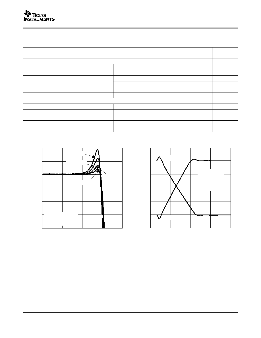
TYPICAL CHARACTERISTICS
Table of Graphs
-1.5
-1
-0.5
0
0.5
1
1.5
0
20
40
60
80
t - Time - ns
V
DD
= 3.3 V,
V
O
= 2 V
PP
,
T
A
= 25
∞
C
G = 1
R
L
= 800
- Output V
oltage - V
V
O
Rising Edge
Falling Edge
-4
-2
-1
0
1
2
100 k
1M
10 M
100 M
1G
G = 1
V
I
= 22.5 mV
RMS
V
DD
= 3.3 V
R
f
= 270
R
f
= 200
Gain - dB
f - Frequency - Hz
R
f
= 390
R
f
= 150
-3
THS4120
THS4121
SLOS319D ≠ FEBRUARY 2001 ≠ REVISED OCTOBER 2004
FIGURE
Small-signal frequency response
1
SR
Slew rate
2
vs Frequency
3
THD
Total harmonic distortion
vs Output voltage
4
vs Frequency
5, 6, 7
Harmonic distortion
vs Output voltage
8, 9
Third intermodulation distortion
vs Output voltage
10
V
O
Output voltage
vs Load resistance
11
Settling time
12
V
n
Voltage noise
vs Frequency
13
V
OO
Output offset voltage
vs Common-mode input voltage
14
CMMR
Common-mode rejection ratio
vs Frequency
15
z
os
Single-ended output impedance (closed loop)
vs Frequency
16
z
o
Single-ended (V
OCM
) input impedance
vs Frequency
17
SMALL-SIGNAL FREQUENCY RESPONSE
SLEW RATE
Figure 1.
Figure 2.
5