 | –≠–ª–µ–∫—Ç—Ä–æ–Ω–Ω—ã–π –∫–æ–º–ø–æ–Ω–µ–Ω—Ç: TL051AM | –°–∫–∞—á–∞—Ç—å:  PDF PDF  ZIP ZIP |
TL05x, TL05xA
ENHANCED-JFET LOW-OFFSET
OPERATIONAL AMPLIFIERS
SLOS178A ≠ FEBRUARY 1997 - REVISED FEBRUARY 2003
1
POST OFFICE BOX 655303
∑
DALLAS, TEXAS 75265
D
Direct Upgrades to TL07x and TL08x BiFET
Operational Amplifiers
D
Faster Slew Rate (20 V/
µ
s Typ) Without
Increased Power Consumption
D
On-Chip Offset-Voltage Trimming for
Improved DC Performance and Precision
Grades Are Available (1.5 mV, TL051A)
1
2
3
4
5
6
7
14
13
12
11
10
9
8
1OUT
1IN≠
1IN+
V
CC+
2IN+
2IN≠
2OUT
4OUT
4IN≠
4IN+
V
CC≠
3IN+
3IN≠
3OUT
1
2
3
4
8
7
6
5
OFFSET N1
IN≠
IN+
V
CC≠
NC
V
CC+
OUT
OFFSET N2
1
2
3
4
8
7
6
5
1OUT
1IN≠
1IN+
V
CC≠
V
CC+
2OUT
2IN≠
2IN+
TL054
D, DB, N, OR NS PACKAGE
(TOP VIEW)
TL051
D OR P PACKAGE
(TOP VIEW)
TL052
D, P, OR PS PACKAGE
(TOP VIEW)
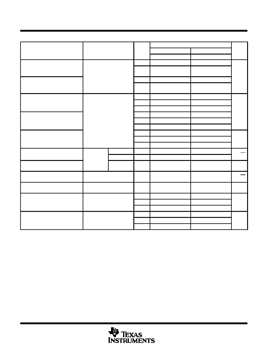
description/ordering information
The TL05x series of JFET-input operational amplifiers offers improved dc and ac characteristics over the TL07x
and TL08x families of BiFET operational amplifiers. On-chip Zener trimming of offset voltage yields precision
grades as low as 1.5 mV (TL051A) for greater accuracy in dc-coupled applications. Texas Instruments improved
BiFET process and optimized designs also yield improved bandwidth and slew rate without increased power
consumption. The TL05x devices are pin-compatible with the TL07x and TL08x and can be used to upgrade
existing circuits or for optimal performance in new designs.
BiFET operational amplifiers offer the inherently higher input impedance of the JFET-input transistors, without
sacrificing the output drive associated with bipolar amplifiers. This makes them better suited for interfacing with
high-impedance sensors or very low-level ac signals. They also feature inherently better ac response than
bipolar or CMOS devices having comparable power consumption.
The TL05x family was designed to offer higher precision and better ac response than the TL08x, with the low
noise floor of the TL07x. Designers requiring significantly faster ac response or ensured lower noise should
consider the Excalibur TLE208x and TLE207x families of BiFET operational amplifiers.
Because BiFET operational amplifiers are designed for use with dual power supplies, care must be taken to
observe common-mode input voltage limits and output swing when operating from a single supply. DC biasing
of the input signal is required, and loads should be terminated to a virtual-ground node at mid-supply. Texas
Instruments TLE2426 integrated virtual ground generator is useful when operating BiFET amplifiers from single
supplies.
The TL05x are fully specified at
±
15 V and
±
5 V. For operation in low-voltage and/or single-supply systems,
Texas Instruments LinCMOS families of operational amplifiers (TLC-prefix) are recommended. When moving
from BiFET to CMOS amplifiers, particular attention should be paid to the slew rate and bandwidth
requirements, and also the output loading.
Please be aware that an important notice concerning availability, standard warranty, and use in critical applications of
Texas Instruments semiconductor products and disclaimers thereto appears at the end of this data sheet.
Copyright
2003, Texas Instruments Incorporated
PRODUCTION DATA information is current as of publication date.
Products conform to specifications per the terms of Texas Instruments
standard warranty. Production processing does not necessarily include
testing of all parameters.
TL05x, TL05xA
ENHANCED-JFET LOW-OFFSET
OPERATIONAL AMPLIFIERS
SLOS178A ≠ FEBRUARY 1997 - REVISED FEBRUARY 2003
2
POST OFFICE BOX 655303
∑
DALLAS, TEXAS 75265
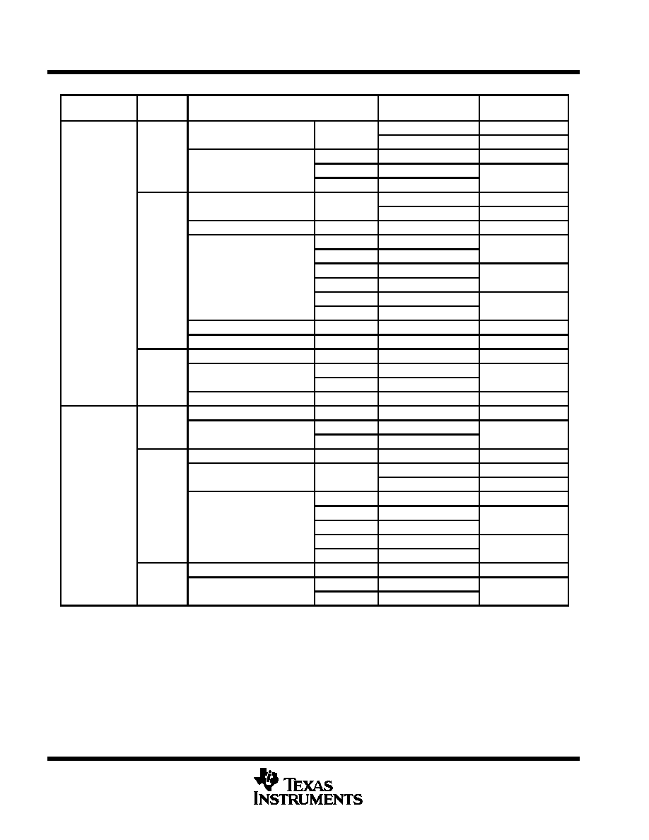
ORDERING INFORMATION
TA
VIOmax
AT 25
∞
C
PACKAGE
ORDERABLE
PART NUMBER
TOP-SIDE
MARKING
PDIP (P)
Tube of 50
TL051ACP
TL051ACP
PDIP (P)
Tube of 50
TL052ACP
TL052ACP
800
µ
V
Tube of 75
TL051ACD
051AC
SOIC (D)
Tube of 75
TL052ACD
052AC
Reel of 2500
TL052ACDR
052AC
PDIP (P)
Tube of 50
TL051CP
TL051CP
PDIP (P)
Tube of 50
TL052CP
TL052CP
PDIP (N)
Tube of 25
TL054ACN
TL054ACN
Tube of 75
TL051CD
TL051C
0
∞
C to 70
∞
C
Reel of 2500
TL051CDR
TL051C
0
∞
C to 70
∞
C
1.5 mV
SOIC (D)
Tube of 75
TL052CD
TL052C
SOIC (D)
Reel of 2500
TL052CDR
TL052C
Tube of 50
TL054ACD
TL054C
Reel of 2500
TL054ACDR
TL054C
SOP (PS)
Reel of 2000
TL052CPSR
TL052
SSOP (DB)
Reel of 2000
TL054CDBR
TL054
PDIP (N)
Tube of 25
TL054CN
TL054CN
4 mV
SOIC (D)
Tube of 50
TL054CD
TL054C
4 mV
SOIC (D)
Reel of 2500
TL054CDR
TL054C
SOP (NS)
Reel of 2000
TL054CNSR
TL054
PDIP (P)
Tube of 50
TL052AIP
TL052AI
800
µ
V
SOIC (D)
Tube of 75
TL052AID
052AI
SOIC (D)
Reel of 2500
TL052AIDR
052AI
PDIP (N)
Tube of 25
TL054AIN
TL054AIN
PDIP (P)
Tube of 50
TL051IP
TL051IP
PDIP (P)
Tube of 50
TL052IP
TL052IP
40
∞
C to 85
∞
C
1 5 mV
Tube of 75
TL051ID
TL051I
≠40
∞
C to 85
∞
C
1.5 mV
Tube of 75
TL052ID
TL052I
SOIC (D)
Reel of 2500
TL052IDR
TL052I
Tube of 50
TL054AID
TL054AI
Reel of 2500
TL054AIDR
TL054AI
PDIP (N)
Tube of 25
TL054IN
TL054IN
4 mV
SOIC (D)
Tube of 50
TL054ID
TL054I
SOIC (D)
Reel of 2500
TL054IDR
TL054I
Package drawings, standard packing quantities, thermal data, symbolization, and PCB design guidelines are available at
www.ti.com/sc/package.
TL05x, TL05xA
ENHANCED-JFET LOW-OFFSET
OPERATIONAL AMPLIFIERS
SLOS178A ≠ FEBRUARY 1997 - REVISED FEBRUARY 2003
3
POST OFFICE BOX 655303
∑
DALLAS, TEXAS 75265
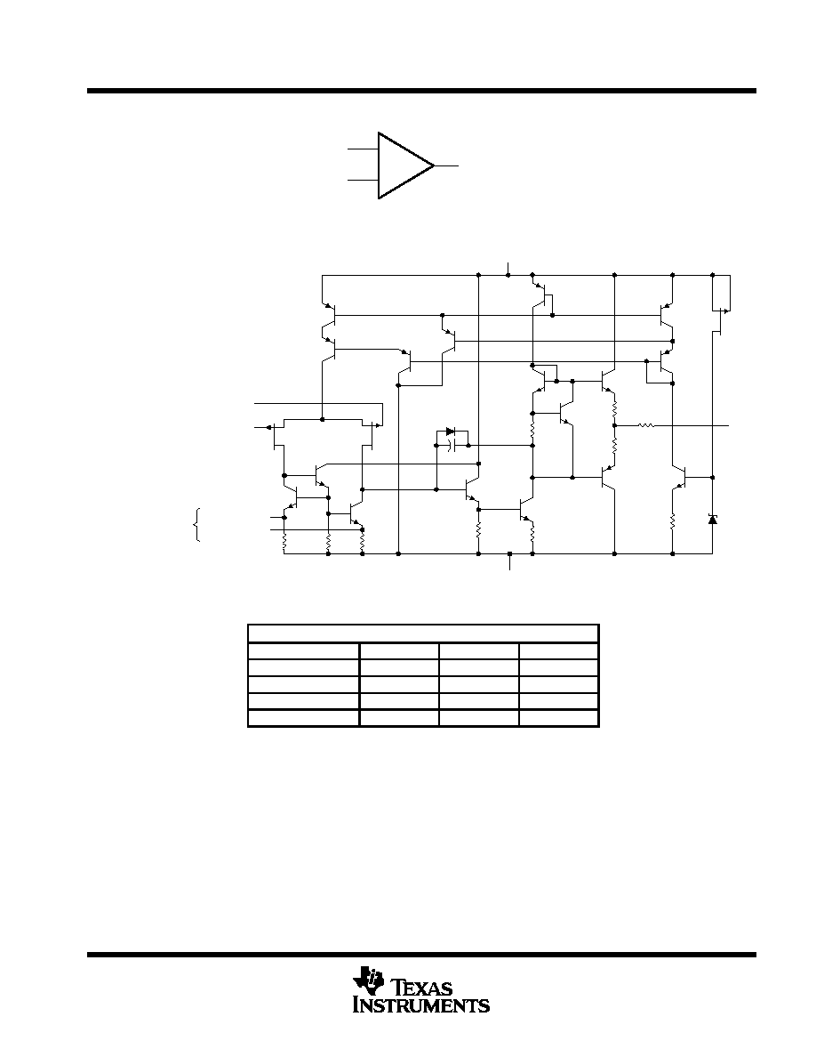
symbol (each amplifier)
+
≠
IN≠
IN+
OUT
equivalent schematic (each amplifier)
R9
OFFSET N2
OFFSET N1
IN≠
IN+
Q2
Q3
Q7
VCC+
Q14
Q6
R4
Q8
Q10
R7
Q11
R6
C1
Q9
Q5
Q4
R5
R1
Q1
JF1
JF2
Q13
Q16
R8
JF3
Q15
Q17
OUT
VCC≠
R2
R3
Q12
R10
D2
D1
See Note A
NOTE A: OFFSET N1 and OFFSET N2 are available only on the TL051x.
ACTUAL DEVICE COMPONENT COUNT
COMPONENT
TL051
TL052
TL054
Transistors
20
34
62
Resistors
10
19
37
Diodes
2
3
5
Capacitors
1
2
4
These figures include all four amplifiers and all ESD, bias, and trim circuitry.

TL05x, TL05xA
ENHANCED-JFET LOW-OFFSET
OPERATIONAL AMPLIFIERS
SLOS178A ≠ FEBRUARY 1997 - REVISED FEBRUARY 2003
4
POST OFFICE BOX 655303
∑
DALLAS, TEXAS 75265
absolute maximum ratings over operating free-air temperature range (unless otherwise noted)
Supply voltage, V
CC+
(see Note 1)
18 V
. . . . . . . . . . . . . . . . . . . . . . . . . . . . . . . . . . . . . . . . . . . . . . . . . . . . . . . . . . .
Supply voltage, V
CC≠
(see Note 1)
≠18 V
. . . . . . . . . . . . . . . . . . . . . . . . . . . . . . . . . . . . . . . . . . . . . . . . . . . . . . . . . .
Differential input voltage (see Note 2)
±
30 V
. . . . . . . . . . . . . . . . . . . . . . . . . . . . . . . . . . . . . . . . . . . . . . . . . . . . . . . .
Input voltage range, V
I
(any input, see Notes 1 and 3)
±
15 V
. . . . . . . . . . . . . . . . . . . . . . . . . . . . . . . . . . . . . . . . .
Input current, I
I
(each input)
±
1 mA
. . . . . . . . . . . . . . . . . . . . . . . . . . . . . . . . . . . . . . . . . . . . . . . . . . . . . . . . . . . . . . .
Output current, I
O
(each output)
±
80 mA
. . . . . . . . . . . . . . . . . . . . . . . . . . . . . . . . . . . . . . . . . . . . . . . . . . . . . . . . . .
Total current into V
CC+
160 mA
. . . . . . . . . . . . . . . . . . . . . . . . . . . . . . . . . . . . . . . . . . . . . . . . . . . . . . . . . . . . . . . . . .
Total current out of V
CC≠
160 mA
. . . . . . . . . . . . . . . . . . . . . . . . . . . . . . . . . . . . . . . . . . . . . . . . . . . . . . . . . . . . . . . . .
Duration of short-circuit current at (or below) 25
∞
C Unlimited
. . . . . . . . . . . . . . . . . . . . . . . . . . . . . . . . . . . . . . . . .
Package thermal impedance,
JA
(see Notes 4 and 5): D package (8 pin)
97
∞
C/W
. . . . . . . . . . . . . . . . . . . . . .
D package (14 pin)
86
∞
C/W
. . . . . . . . . . . . . . . . . . . . .
DB package (14 pin)
96
∞
C/W
. . . . . . . . . . . . . . . . . . .
N package (14 pin)
80
∞
C/W
. . . . . . . . . . . . . . . . . . . . .
NS package (14 pin)
76
∞
C/W
. . . . . . . . . . . . . . . . . . .
P package (8 pin)
85
∞
C/W
. . . . . . . . . . . . . . . . . . . . . .
PS package (8 pin)
95
∞
C/W
. . . . . . . . . . . . . . . . . . . .
Operating virtual junction temperature, T
J
150
∞
C
. . . . . . . . . . . . . . . . . . . . . . . . . . . . . . . . . . . . . . . . . . . . . . . . . . .
Lead temperature 1,6 mm (1/16inch) from case for 10 seconds
260
∞
C
. . . . . . . . . . . . . . . . . . . . . . . . . . . . . . . .
Storage temperature range
≠65
∞
C to 150
∞
C
. . . . . . . . . . . . . . . . . . . . . . . . . . . . . . . . . . . . . . . . . . . . . . . . . . . . . . . .
Stresses beyond those listed under "absolute maximum ratings" may cause permanent damage to the device. These are stress ratings only, and
functional operation of the device at these or any other conditions beyond those indicated under "recommended operating conditions" is not
implied. Exposure to absolute-maximum-rated conditions for extended periods may affect device reliability.
NOTES:
1. All voltage values, except differential voltages, are with respect to the midpoint between VCC+ and VCC≠.
2. Differential voltages are at IN+ with respect to IN≠.
3. The magnitude of the input voltage must never exceed the magnitude of the supply voltage or 15 V, whichever is less.
4. Maximum power dissipation is a function of TJ(max),
JA, and TA. The maximum allowable power dissipation at any allowable
ambient temperature is PD = (TJ(max) ≠ TA)/
JA. Operating at the absolute maximum TJ of 150
∞
C can impact reliability.
5. The package thermal impedance is calculated in accordance with JESD 51-7.
recommended operating conditions
C SUFFIX
I SUFFIX
UNIT
MIN
MAX
MIN
MAX
UNIT
VCC
±
Supply voltage
±
5
±
15
±
5
±
15
V
VIC
Common mode input voltage
VCC
±
=
±
5 V
≠1
4
≠1
4
V
VIC
Common-mode input voltage
VCC
±
=
±
15 V
≠11
11
≠11
11
V
TA
Operating free-air temperature
0
70
≠40
85
∞
C
TL05x, TL05xA
ENHANCED-JFET LOW-OFFSET
OPERATIONAL AMPLIFIERS
SLOS178A ≠ FEBRUARY 1997 - REVISED FEBRUARY 2003
5
POST OFFICE BOX 655303
∑
DALLAS, TEXAS 75265
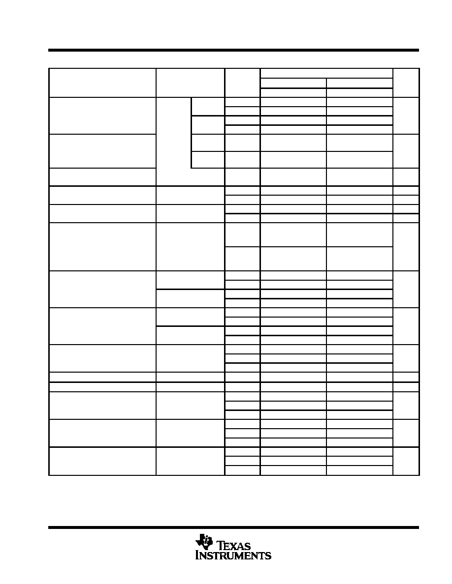
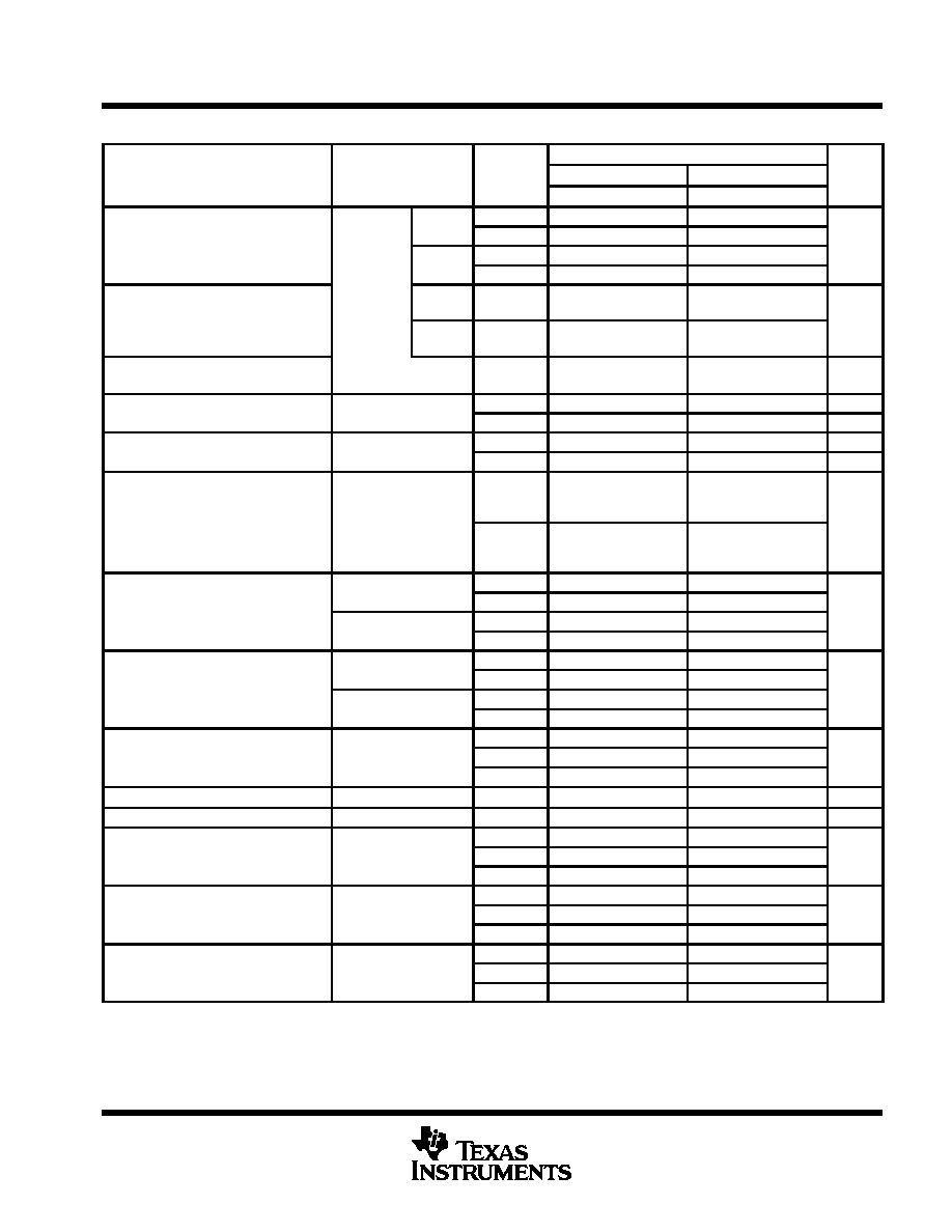
TL051C and TL051AC electrical characteristics at specified free-air temperature
TL051C, TL051AC
PARAMETER
TEST CONDITIONS
TA
VCC
±
=
±
5 V
VCC
±
=
±
15 V
UNIT
MIN
TYP
MAX
MIN
TYP
MAX
TL051C
25
∞
C
0.75
3.5
0.59
1.5
VIO
Input offset voltage
TL051C
Full range
4.5
2.5
mV
VIO
Input offset voltage
TL051AC
25
∞
C
0.55
2.8
0.35
0.8
mV
VO = 0
TL051AC
Full range
3.8
1.8
a
Temperature coefficient
VO = 0,
VIC = 0,
RS = 50
TL051C
25
∞
C to
70
∞
C
8
8
µ
V/
∞
C
a
V
IO
of input offset voltage
RS = 50
TL051AC
25
∞
C to
70
∞
C
8
8
25
µ
V/
∞
C
Input offset-voltage
long-term driftß
25
∞
C
0.04
0.04
µ
V/mo
IIO
Input offset current
VO = 0,
VIC = 0,
25
∞
C
4
100
5
100
pA
IIO
Input offset current
O
IC
See Figure 5
70
∞
C
0.02
1
0.025
1
nA
IIB
Input bias current
VO = 0,
VIC = 0,
25
∞
C
20
200
30
200
pA
IIB
Input bias current
O
IC
See Figure 5
70
∞
C
0.15
4
0.2
4
nA
VICR
Common-mode input
25
∞
C
≠1
to
4
≠2.3
to
5.6
≠11
to
11
≠12.3
to
15.6
V
VICR
voltage range
Full range
≠1
to
4
≠11
to
11
V
RL = 10 k
25
∞
C
3
4.2
13
13.9
VOM
Maximum positive peak
RL = 10 k
Full range
3
13
V
VOM+
output voltage swing
RL = 2 k
25
∞
C
2.5
3.8
11.5
12.7
V
RL = 2 k
Full range
2.5
11.5
RL = 10 k
25
∞
C
≠2.5
≠3.5
≠12
≠13.2
VOM
Maximum negative peak
RL = 10 k
Full range
≠2.5
≠12
V
VOM≠
g
output voltage swing
RL = 2 k
25
∞
C
≠2.3
≠3.2
≠11
≠12
V
RL = 2 k
Full range
≠2.3
≠11
L
i
l diff
ti l
25
∞
C
25
59
50
105
AVD
Large-signal differential
voltage amplification∂
RL = 2 k
0
∞
C
30
65
60
129
V/mV
voltage am lification∂
70
∞
C
20
46
30
85
ri
Input resistance
25
∞
C
1012
1012
ci
Input capacitance
25
∞
C
10
12
pF
Common mode
V
V
min
25
∞
C
65
85
75
93
CMRR
Common-mode
rejection ratio
VIC = VICRmin,
VO = 0
RS = 50
0
∞
C
65
84
75
92
dB
rejection ratio
VO = 0,
RS = 50
70
∞
C
65
84
75
91
Supply voltage rejection
25
∞
C
75
99
75
99
kSVR
Supply-voltage rejection
ratio (
VCC
±
/
VIO)
VO = 0,
RS = 50
0
∞
C
75
98
75
98
dB
ratio (
VCC
±
/
VIO)
70
∞
C
75
97
75
97
25
∞
C
2.6
3.2
2.7
3.2
ICC
Supply current
VO = 0,
No load
0
∞
C
2.7
3.2
2.8
3.2
mA
CC
y
O
70
∞
C
2.6
3.2
2.7
3.2
Full range is 0
∞
C to 70
∞
C.
This parameter is tested on a sample basis for the TL051A. For other test requirements, please contact the factory. This statement has no bearing
on testing or nontesting of other parameters.
ß Typical values are based on the input offset-voltage shift observed through 168 hours of operating life test at TA = 150
∞
C, extrapolated to
TA = 25
∞
C using the Arrhenius equation, and assuming an activation energy of 0.96 eV.
∂ For VCC
±
=
±
5 V, VO =
±
2.3 V, or for VCC
±
=
±
15 V, VO =
±
10 V.
TL05x, TL05xA
ENHANCED-JFET LOW-OFFSET
OPERATIONAL AMPLIFIERS
SLOS178A ≠ FEBRUARY 1997 - REVISED FEBRUARY 2003
6
POST OFFICE BOX 655303
∑
DALLAS, TEXAS 75265
TL051C and TL051AC operating characteristics at specified free-air temperature
TL051C, TL051AC
PARAMETER
TEST CONDITIONS
TA
VCC
±
=
±
5 V
VCC
±
=
±
15 V
UNIT
MIN
TYP
MAX
MIN
TYP
MAX
P
iti
l
t
25
∞
C
16
13
20
SR+
Positive slew rate
at unity gain
RL = 2 k
,
CL = 100 pF,
Full
range
16.4
11
22.6
V/
µ
s
N
ti
l
t
L
,
L
,
See Figure 1
25
∞
C
15
13
18
V/
µ
s
SR≠
Negative slew rate
at unity gain
Full
range
16
11
19.3
25
∞
C
55
56
tr
Rise time
0
∞
C
54
55
70
∞
C
63
63
ns
VI(PP) =
±
10 mV,
R
2 k
25
∞
C
55
57
ns
tf
Fall time
RL = 2 k
,
CL = 100 pF
0
∞
C
54
56
CL = 100 F,
See Figures 1 and 2
70
∞
C
62
64
g
25
∞
C
24
19
Overshoot factor
0
∞
C
24
19
%
70
∞
C
24
19
V
Equivalent input noise
f = 10 Hz
25
∞
C
75
75
nV/
Hz
Vn
q
voltageß
RS = 20
,
f = 1 kHz
25
∞
C
18
18
30
nV/
Hz
VN(PP)
Peak-to-peak equivalent
input noise voltage
See Figure 3
f = 10 Hz to
10 kHz
25
∞
C
4
4
µ
V
In
Equivalent input
noise current
f = 1 kHz
25
∞
C
0.01
0.01
pA/
Hz
THD
Total harmonic distortion∂
RS = 1 k
,
f = 1 kHz
RL = 2 k
,
25
∞
C
0.003
0.003
%
V
10
V
R
2 k
25
∞
C
3
3.1
B1
Unity-gain bandwidth
VI = 10 mV,
RL = 2 k
,
CL = 25 pF
See Figure 4
0
∞
C
3.2
3.3
MHz
CL = 25 F,
See Figure 4
70
∞
C
2.7
2.8
Phase margin at unity
V
10 mV
R
2 k
25
∞
C
59
62
m
Phase margin at unity
gain
VI = 10 mV,
RL = 2 k
,
CL = 25 pF,
See Figure 4
0
∞
C
58
62
deg
gain
CL = 25 F,
See Figure 4
70
∞
C
59
62
Full range is 0
∞
C to 70
∞
C.
For VCC
±
=
±
5 V, VI(PP) =
±
1 V; for VCC
±
=
±
15 V, VI(PP) =
±
5 V.
ß This parameter is tested on a sample basis for the TL051A. For other test requirements, please contact the factory. This statement has no bearing
on testing or nontesting of other parameters.
∂ For VCC
±
=
±
5 V, VO(RMS) = 1 V; for VCC
±
=
±
15 V, VO(RMS) = 6 V.
TL05x, TL05xA
ENHANCED-JFET LOW-OFFSET
OPERATIONAL AMPLIFIERS
SLOS178A ≠ FEBRUARY 1997 - REVISED FEBRUARY 2003
7
POST OFFICE BOX 655303
∑
DALLAS, TEXAS 75265
TL051I and TL051AI electrical characteristics at specified free-air temperature
TL051I, TL051AI
PARAMETER
TEST CONDITIONS
TA
VCC
±
=
±
5 V
VCC
±
=
±
15 V
UNIT
A
MIN
TYP
MAX
MIN
TYP
MAX
TL051I
25
∞
C
0.75
3.5
0.59
1.5
VIO
Input offset voltage
TL051I
Full range
5.3
3.3
mV
VIO
Input offset voltage
TL051AI
25
∞
C
0.55
2.8
0.35
0.8
mV
VO = 0
TL051AI
Full range
4.6
2.6
a
Temperature coefficient of
VO = 0,
VIC = 0,
RS = 50
TL051I
25
∞
C to
85
∞
C
7
8
µ
V/
∞
C
a
V
IO
input offset voltage
RS = 50
TL051AI
25
∞
C to
85
∞
C
8
8
25
µ
V/
∞
C
Input offset-voltage
long-term driftß
25
∞
C
0.04
0.04
µ
V/mo
IIO
Input offset current
VO = 0,
VIC = 0,
25
∞
C
4
100
5
100
pA
IIO
Input offset current
O
IC
See Figure 5
85
∞
C
0.06
10
0.07
10
nA
IIB
Input bias current
VO = 0,
VIC = 0,
25
∞
C
20
200
30
200
pA
IIB
Input bias current
O
IC
See Figure 5
85
∞
C
0.6
20
0.7
20
nA
VICR
Common-mode input
25
∞
C
≠1
to
4
≠2.3
to
5.6
≠11
to
11
≠12.3
to
15.6
V
VICR
voltage range
Full range
≠1
to
4
≠11
to
11
V
RL = 10 k
25
∞
C
3
4.2
13
13.9
VOM
Maximum positive peak
RL = 10 k
Full range
3
13
V
VOM +
output voltage swing
RL = 2 k
25
∞
C
2.5
3.8
11.5
12.7
V
RL = 2 k
Full range
2.5
11.5
RL = 10 k
25
∞
C
≠2.5
≠3.5
≠12
≠13.2
VOM
Maximum negative peak
RL = 10 k
Full range
≠2.5
≠12
V
VOM ≠
g
output voltage swing
RL = 2 k
25
∞
C
≠2.3
≠3.2
≠11
≠12
V
RL = 2 k
Full range
≠2.3
≠11
L
i
l diff
ti l
25
∞
C
25
59
50
105
AVD
Large-signal differential
voltage amplification∂
RL = 2 k
≠40
∞
C
30
74
60
145
V/mV
voltage am lification∂
85
∞
C
20
43
30
76
ri
Input resistance
25
∞
C
1012
1012
ci
Input capacitance
25
∞
C
10
12
pF
Common mode
VIC = VICRmin,
25
∞
C
65
85
75
93
CMRR
Common-mode
rejection ratio
VIC VICRmin,
VO = 0,
≠40
∞
C
65
83
75
90
dB
rejection ratio
RS = 50
85
∞
C
65
84
75
93
Supply voltage rejection
V
0
25
∞
C
75
99
75
99
kSVR
Supply-voltage rejection
ratio (
VCC
±
/
VIO)
VO = 0,
RS = 50
≠40
∞
C
75
98
75
98
dB
ratio (
VCC
±
/
VIO)
RS = 50
85
∞
C
75
99
75
99
25
∞
C
2.6
3.2
2.7
3.2
ICC
Supply current
VO = 0,
No load
≠40
∞
C
2.4
3.2
2.6
3.2
mA
85
∞
C
2.5
3.2
2.6
3.2
Full range is ≠40
∞
C to 85
∞
C
This parameter is tested on a sample basis for the TL051A. For other test requirements, please contact the factory. This statement has no bearing
on testing or nontesting of other parameters.
ß Typical values are based on the input offset-voltage shift observed through 168 hours of operating life test at TA = 150
∞
C, extrapolated to
TA = 25
∞
C using the Arrhenius equation, and assuming an activation energy of 0.96 eV.
∂ For VCC
±
=
±
5 V, VO =
±
2.3 V, or for VCC
±
=
±
15 V, VO =
±
10 V.

TL05x, TL05xA
ENHANCED-JFET LOW-OFFSET
OPERATIONAL AMPLIFIERS
SLOS178A ≠ FEBRUARY 1997 - REVISED FEBRUARY 2003
8
POST OFFICE BOX 655303
∑
DALLAS, TEXAS 75265
TL051I and TL051AI operating characteristics at specified free-air temperature
TL051I, TL051AI
PARAMETER
TEST CONDITIONS
TA
VCC
±
=
±
5 V
VCC
±
=
±
15 V
UNIT
MIN
TYP
MAX
MIN
TYP
MAX
P
iti
l
t
25
∞
C
16
13
20
SR+
Positive slew rate
at unity gain
RL = 2 k
,
CL = 100 pF,
Full
range
11
V/
µ
s
N
ti
l
t
L
,
L
,
See Figure 1
25
∞
C
15
13
18
V/
µ
s
SR≠
Negative slew rate
at unity gain
Full
range
11
25
∞
C
55
56
tr
Rise time
≠40
∞
C
52
53
85
∞
C
64
65
ns
VI(PP) =
±
10 mV,
R
2 k
25
∞
C
55
57
ns
tf
Fall time
(
)
RL = 2 k
,
CL = 100 pF
≠40
∞
C
51
53
CL = 100 F,
See Figures 1 and 2
85
∞
C
64
65
g
25
∞
C
24
19
Overshoot factor
≠40
∞
C
24
19
%
85
∞
C
24
19
V
Equivalent input noise
f = 10 Hz
25
∞
C
75
75
nV/
Hz
Vn
q
voltageß
RS = 20
,
f = 1 kHz
25
∞
C
18
18
30
nV/
Hz
VN(PP)
Peak-to-peak equivalent
input noise voltage
See Figure 3
f = 10 Hz to
10 kHz
25
∞
C
4
4
µ
V
In
Equivalent input
noise current
f = 1 kHz
25
∞
C
0.01
0.01
pA/
Hz
THD
Total harmonic distortion∂
RS = 1 k
,
f = 1 kHz
RL = 2 k
,
25
∞
C
0.003
0.003
%
V
10
V
R
2 k
25
∞
C
3
3.1
B1
Unity-gain bandwidth
VI = 10 mV,
RL = 2 k
,
CL = 25 pF
See Figure 4
≠40
∞
C
3.5
3.6
MHz
CL = 25 F,
See Figure 4
85
∞
C
2.6
2.7
Phase margin at unity
V
10 mV
R
2 k
25
∞
C
59
62
m
Phase margin at unity
gain
VI = 10 mV,
RL = 2 k
,
CL = 25 pF,
See Figure 4
≠40
∞
C
58
61
deg
gain
CL = 25 F,
See Figure 4
85
∞
C
59
62
Full range is ≠40
∞
C to 85
∞
C.
For VCC
±
=
±
5 V, VI(PP) =
±
1 V; for VCC
±
=
±
15 V, VI(PP) =
±
5 V.
ß This parameter is tested on a sample basis for the TL051A. For other test requirements, please contact the factory. This statement has no bearing
on testing or nontesting of other parameters.
∂ For VCC
±
=
±
5 V, VO(RMS) = 1 V; for VCC
±
=
±
15 V, VO(RMS) = 6 V.

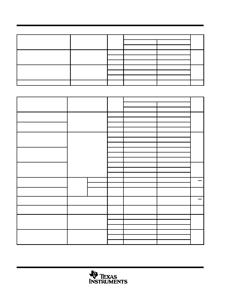
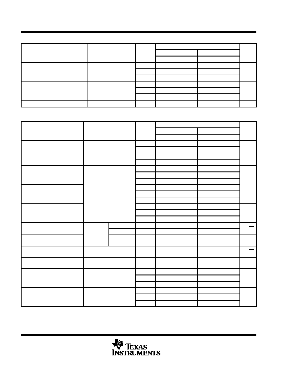
TL05x, TL05xA
ENHANCED-JFET LOW-OFFSET
OPERATIONAL AMPLIFIERS
SLOS178A ≠ FEBRUARY 1997 - REVISED FEBRUARY 2003
9
POST OFFICE BOX 655303
∑
DALLAS, TEXAS 75265
TL052C and TL052AC electrical characteristics at specified free-air temperature
TL052C, TL052AC
PARAMETER
TEST CONDITIONS
TA
VCC
±
=
±
5 V
VCC
±
=
±
15 V
UNIT
A
MIN
TYP
MAX
MIN
TYP
MAX
TL052C
25
∞
C
0.73
3.5
0.65
1.5
VIO
Input offset voltage
TL052C
Full range
4.5
2.5
mV
VIO
Input offset voltage
V
0
TL052AC
25
∞
C
0.51
2.8
0.4
0.8
mV
VO = 0,
VIC = 0
TL052AC
Full range
3.8
1.8
VIC = 0,
RS = 50
TL052C
25
∞
C to
8
8
a
Temperature coefficient
RS 50
TL052C
70
∞
C
8
8
µ
V/
∞
C
a
V
IO
of input offset voltage
TL052AC
25
∞
C to
8
6
25
µ
V/
∞
C
TL052AC
70
∞
C
8
6
25
Input offset-voltage
long-term driftß
VO = 0,
RS = 50
VIC = 0,
25
∞
C
0.04
0.04
µ
V/mo
IIO
Input offset current
VO = 0,
VIC = 0
25
∞
C
4
100
5
100
pA
IIO
Input offset current
O
,
See Figure 5
VIC = 0,
70
∞
C
0.02
1
0.025
1
nA
IIB
Input bias current
VO = 0,
VIC = 0
25
∞
C
20
200
30
200
pA
IIB
Input bias current
O
,
See Figure 5
VIC = 0,
70
∞
C
0.15
4
0.2
4
nA
VICR
Common-mode input
25
∞
C
≠1
to
4
≠2.3
to
5.6
≠11
to
11
≠12.3
to
15.6
V
VICR
voltage range
Full range
≠1
to
4
≠11
to
11
V
RL = 10 k
25
∞
C
3
4.2
13
13.9
VOM
Maximum positive peak
RL = 10 k
Full range
3
13
V
VOM+
output voltage swing
RL = 2 k
25
∞
C
2.5
3.8
11.5
12.7
V
RL = 2 k
Full range
2.5
11.5
RL = 10 k
25
∞
C
≠2.5
≠3.5
≠12
≠13.2
VOM
Maximum negative peak
RL = 10 k
Full range
≠2.5
≠12
V
VOM≠
g
output voltage swing
RL = 2 k
25
∞
C
≠2.3
≠3.2
≠11
≠12
V
RL = 2 k
Full range
≠2.3
≠11
L
i
l diff
ti l
25
∞
C
25
59
50
105
AVD
Large-signal differential
voltage amplification∂
RL = 2 k
0
∞
C
30
65
60
129
V/mV
voltage am lification∂
70
∞
C
20
46
30
85
ri
Input resistance
25
∞
C
1012
1012
ci
Input capacitance
25
∞
C
10
12
pF
Common mode
V
V
min
25
∞
C
65
85
75
93
CMRR
Common-mode
rejection ratio
VIC = VICRmin,
VO = 0,
RS = 50
0
∞
C
65
84
75
92
dB
rejection ratio
VO = 0,
70
∞
C
65
84
75
91
Full range is 0
∞
C to 70
∞
C.
This parameter is tested on a sample basis. For other test requirements, please contact the factory. This statement has no bearing on testing
or nontesting of other parameters.
ß Typical values are based on the input offset-voltage shift observed through 168 hours of operating life test at TA = 150
∞
C, extrapolated to
TA = 25
∞
C using the Arrhenius equation, and assuming an activation energy of 0.96 eV.
∂ For VCC
±
=
±
5 V, VO =
±
2.3 V; at VCC
±
=
±
15 V, VO =
±
10 V.
TL05x, TL05xA
ENHANCED-JFET LOW-OFFSET
OPERATIONAL AMPLIFIERS
SLOS178A ≠ FEBRUARY 1997 - REVISED FEBRUARY 2003
10
POST OFFICE BOX 655303
∑
DALLAS, TEXAS 75265
TL052C and TL052AC electrical characteristics at specified free-air temperature (continued)
TL052C, TL052AC
PARAMETER
TEST CONDITIONS
TA
VCC
±
=
±
5 V
VCC
±
=
±
15 V
UNIT
A
MIN
TYP
MAX
MIN
TYP
MAX
S
l
lt
j
ti
25
∞
C
75
99
75
99
kSVR
Supply-voltage rejection
ratio (
VCC
±
/
VIO)
VO = 0,
RS = 50
0
∞
C
75
98
75
98
dB
ratio (
VCC
±
/
VIO)
70
∞
C
75
97
75
97
S
l
t
25
∞
C
4.6
5.6
4.8
5.6
ICC
Supply current
(two amplifiers)
VO = 0,
No load
0
∞
C
4.7
6.4
4.8
6.4
mA
(two am lifiers)
70
∞
C
4.4
6.4
4.6
6.4
VO1/VO2 Crosstalk attenuation
AVD = 100
25
∞
C
120
120
dB
TL052C and TL052AC operating characteristics at specified free-air temperature
TL052C, TL052AC
PARAMETER
TEST CONDITIONS
TA
VCC
±
=
±
5 V
VCC
±
=
±
15 V
UNIT
A
MIN
TYP
MAX
MIN
TYP
MAX
SR+
Slew rate at unity gain
25
∞
C
17.8
9
20.7
SR+
Slew rate at unity gain
RL = 2 k
,
CL = 100 pF, Full range
8
V/
µ
s
SR
Negative slew rate
See Figure 1
25
∞
C
15.4
9
17.8
V/
µ
s
SR≠
g
at unity gain
Full range
8
25
∞
C
55
56
tr
Rise time
0
∞
C
54
55
70
∞
C
63
63
ns
VI(PP) =
±
10 mV,
R
2 k
25
∞
C
55
57
ns
tf
Fall time
(
)
RL = 2 k
,
CL = 100 pF
0
∞
C
54
56
CL = 100 F,
See Figures 1 and 2
70
∞
C
62
64
g
25
∞
C
24
19
Overshoot factor
0
∞
C
24
19
%
70
∞
C
24
19
V
Equivalent input noise
f = 10 Hz
25
∞
C
71
71
nV/
Hz
Vn
q
voltageß
RS = 20
,
f = 1 kHz
25
∞
C
19
19
30
nV/
Hz
VN(PP)
Peak-to-peak equivalent
input noise current
See Figure 3
f = 10 Hz to
10 kHz
25
∞
C
4
4
µ
V
In
Equivalent input
noise current
f = 1 kHz
25
∞
C
0.01
0.01
pA/
Hz
THD
Total harmonic distortion∂
RS = 1 k
,
f = 1 kHz
RL = 2 k
,
25
∞
C
0.003
0.003
%
V
10
V
R
2 k
25
∞
C
3
3
B1
Unity-gain bandwidth
VI = 10 mV,
CL = 25 pF
RL = 2 k
,
See Figure 4
0
∞
C
3.2
3.2
MHz
CL = 25 F,
See Figure 4
70
∞
C
2.6
2.7
Phase margin at unity
V
10 mV
R
2 k
25
∞
C
60
63
m
Phase margin at unity
gain
VI = 10 mV,
CL = 25 pF,
RL = 2 k
,
See Figure 4
0
∞
C
59
63
deg
gain
CL = 25 F,
See Figure 4
70
∞
C
60
63
Full range is 0
∞
C to 70
∞
C.
For VCC
±
=
±
5 V, VI(PP) =
±
1 V; for VCC
±
=
±
15 V, VI(PP) =
±
5 V.
ß This parameter is tested on a sample basis. For other test requirements, please contact the factory. This statement has no bearing on testing
or nontesting of other parameters.
∂ For VCC
±
=
±
5 V, VO(RMS) = 1 V; for VCC
±
=
±
15 V, VO(RMS) = 6 V.

TL05x, TL05xA
ENHANCED-JFET LOW-OFFSET
OPERATIONAL AMPLIFIERS
SLOS178A ≠ FEBRUARY 1997 - REVISED FEBRUARY 2003
11
POST OFFICE BOX 655303
∑
DALLAS, TEXAS 75265
TL052I and TL052AI electrical characteristics at specified free-air temperature
TL052I, TL052AI
PARAMETER
TEST CONDITIONS
TA
VCC
±
=
±
5 V
VCC
±
=
±
15 V
UNIT
A
MIN
TYP
MAX
MIN
TYP
MAX
TL052I
25
∞
C
0.73
3.5
0.65
1.5
VIO
Input offset voltage
TL052I
Full range
5.3
3.3
mV
VIO
Input offset voltage
V
0
TL052AI
25
∞
C
0.51
2.8
0.4
0.8
mV
VO = 0,
VIC = 0,
TL052AI
Full range
4.6
2.6
a
T
t
ffi i
t
VIC = 0,
RS = 50
TL052I
25
∞
C to
85
∞
C
7
6
µ
V/
∞
C
a
V
IO
Temperature coefficient
TL052AI
25
∞
C to
85
∞
C
6
6
25
µ
V/
∞
C
Input offset-voltage
long-term driftß
VO = 0,
RS = 50
VIC = 0,
25
∞
C
0.04
0.04
µ
V/mo
IIO
Input offset current
VO = 0,
VIC = 0,
25
∞
C
4
100
5
100
pA
IIO
Input offset current
O
,
See Figure 5
IC
,
85
∞
C
0.06
10
0.07
10
nA
IIB
Input bias current
VO = 0,
VIC = 0,
25
∞
C
20
200
30
200
pA
IIB
Input bias current
O
,
See Figure 5
IC
,
85
∞
C
0.6
20
0.7
20
nA
VICR
Common-mode input
25
∞
C
≠1
to
4
≠2.3
to
5.6
≠11
to
11
≠12.3
to
15.6
V
VICR
voltage range
Full range
≠1
to
4
≠11
to
11
V
RL = 10 k
25
∞
C
3
4.2
13
13.9
VOM
Maximum positive peak
RL = 10 k
Full range
3
13
V
VOM+
output voltage swing
RL = 2 k
25
∞
C
2.5
3.8
11.5
12.7
V
RL = 2 k
Full range
2.5
11.5
RL = 10 k
25
∞
C
≠2.5
≠3.5
≠12
≠13.2
VOM
Maximum negative peak
RL = 10 k
Full range
≠2.5
≠12
V
VOM≠
g
output voltage swing
RL = 2 k
25
∞
C
≠2.3
≠3.2
≠11
≠12
V
RL = 2 k
Full range
≠2.3
≠11
L
i
l diff
ti l
25
∞
C
25
59
50
105
AVD
Large-signal differential
voltage amplification∂
RL = 2 k
≠40
∞
C
30
74
60
145
V/mV
voltage am lification∂
85
∞
C
20
43
30
76
ri
Input resistance
25
∞
C
1012
1012
ci
Input capacitance
25
∞
C
10
12
pF
Common mode
V
V
min
25
∞
C
65
85
75
93
CMRR
Common-mode
rejection ratio
VIC = VICRmin,
VO = 0,
RS = 50
≠40
∞
C
65
83
75
90
dB
rejection ratio
VO = 0,
85
∞
C
65
84
75
93
Full range is ≠40
∞
C to 85
∞
C.
This parameter is tested on a sample basis. For other test requirements, please contact the factory. This statement has no bearing on testing
or nontesting of other parameters
ß Typical values are based on the input offset-voltage shift observed through 168 hours of operating life test at TA = 150
∞
C, extrapolated to
TA = 25
∞
C using the Arrhenius equation, and assuming an activation energy of 0.96 eV.
∂ At VCC
±
=
±
5 V, VO =
±
2.3 V; at VCC
±
=
±
15 V, VO =
±
10 V.
TL05x, TL05xA
ENHANCED-JFET LOW-OFFSET
OPERATIONAL AMPLIFIERS
SLOS178A ≠ FEBRUARY 1997 - REVISED FEBRUARY 2003
12
POST OFFICE BOX 655303
∑
DALLAS, TEXAS 75265
TL052I and TL052AI electrical characteristics at specified free-air temperature (continued)
TL052I, TL052AI
PARAMETER
TEST CONDITIONS
TA
VCC
±
=
±
5 V
VCC
±
=
±
15 V
UNIT
A
MIN
TYP
MAX
MIN
TYP
MAX
S
l
lt
j
ti
25
∞
C
75
99
75
99
kSVR
Supply-voltage rejection
ratio (
VCC
±
/
VIO)
VO = 0,
RS = 50
≠40
∞
C
75
98
75
98
dB
ratio (
VCC
±
/
VIO)
85
∞
C
75
99
75
99
S
l
t
25
∞
C
4.6
5.6
4.8
5.6
ICC
Supply current
(two amplifiers)
VO = 0,
No load
≠40
∞
C
4.5
6.4
4.7
6.4
mA
(two am lifiers)
85
∞
C
4.4
6.4
4.6
6.4
VO1/VO2 Crosstalk attenuation
AVD = 100
25
∞
C
120
120
dB
TL052I and TL052AI operating characteristics at specified free-air temperature
TL052I, TL052AI
PARAMETER
TEST CONDITIONS
TA
VCC
±
=
±
5 V
VCC
±
=
±
15 V
UNIT
A
MIN
TYP
MAX
MIN
TYP
MAX
SR+
Sl
t
t
it
i
25
∞
C
17.8
9
20.7
SR+
Slew rate at unity gain
RL = 2 k
,
CL = 100 pF,
Full range
8
V/
µ
s
SR
Negative slew rate at
L
,
L
,
See Figure 1
25
∞
C
15.4
9
17.8
V/
µ
s
SR≠
g
unity gain
Full range
8
25
∞
C
55
56
tr
Rise time
≠40
∞
C
52
53
85
∞
C
64
65
ns
VI(PP) =
±
10 mV,
25
∞
C
55
57
ns
tf
Fall time
VI(PP) =
±
10 mV,
RL = 2 k
,
CL = 100 pF,
≠40
∞
C
51
53
See Figures 1 and 2
85
∞
C
64
65
25
∞
C
24%
19%
Overshoot factor
≠40
∞
C
24%
19%
%
85
∞
C
24%
19
V
Equivalent input noise
f = 10 Hz
25
∞
C
71
71
nV/
Hz
Vn
q
voltageß
RS = 20
,
f = 1 kHz
25
∞
C
19
19
30
nV/
Hz
VN(PP)
Peak-to-peak equivalent
input noise current
See Figure 3
f = 10 Hz to
10 kHz
25
∞
C
4
4
µ
V
In
Equivalent input noise
current
f = 1 kHz
25
∞
C
0.01
0.01
pA/
Hz
THD
Total harmonic distortion∂
RS = 1 k
,
f = 1 kHz
RL = 2 k
,
25
∞
C
0.003
0.003
%
V
10
V
R
2 k
25
∞
C
3
3
B1
Unity-gain bandwidth
VI = 10 mV,
CL = 25 pF
RL = 2 k
,
See Figure 4
≠40
∞
C
3.5
3.6
MHz
CL = 25 F,
See Figure 4
85
∞
C
2.5
2.6
Phase margin at unity
V
10 mV
R
2 k
25
∞
C
60
63
m
Phase margin at unity
gain
VI = 10 mV,
CL = 25 pF,
RL = 2 k
,
See Figure 4
≠40
∞
C
58
61
deg
gain
CL = 25 F,
See Figure 4
85
∞
C
60
63
Full range is ≠40
∞
C to 85
∞
C.
For VCC
±
=
±
5 V, VI(PP) =
±
1 V; for VCC
±
=
±
15 V, VI(PP) =
±
5 V.
ß This parameter is tested on a sample basis. For other test requirements, please contact the factory. This statement has no bearing on testing
or nontesting of other parameters.
∂ For VCC
±
=
±
5 V, VO(RMS) = 1 V; for VCC
±
=
±
15 V, VO(RMS) = 6 V.
TL05x, TL05xA
ENHANCED-JFET LOW-OFFSET
OPERATIONAL AMPLIFIERS
SLOS178A ≠ FEBRUARY 1997 - REVISED FEBRUARY 2003
13
POST OFFICE BOX 655303
∑
DALLAS, TEXAS 75265
TL054C and TL054AC electrical characteristics at specified free-air temperature
TL054C, TL054AC
PARAMETER
TEST CONDITIONS
TA
VCC
±
=
±
5 V
VCC
±
=
±
15 V
UNIT
MIN
TYP
MAX
MIN
TYP
MAX
TL054C
25
∞
C
0.64
5.5
0.56
4
VIO
Input offset voltage
TL054C
Full range
7.7
6.2
mV
VIO
Input offset voltage
TL054AC
25
∞
C
0.57
3.5
0.5
1.5
mV
VO = 0
TL054AC
Full range
5.7
3.7
a
Temperature coefficient
VO = 0,
VIC = 0,
RS = 50
TL054C
25
∞
C to
70
∞
C
25
23
µ
V/
∞
C
a
V
IO
of input offset voltage
RS 50
TL054AC
25
∞
C to
70
∞
C
24
23
µ
V/
∞
C
Input offset-voltage
long-term drift
25
∞
C
0.04
0.04
µ
V/mo
IIO
Input offset current
VO = 0,
VIC = 0,
25
∞
C
4
100
5
100
pA
IIO
Input offset current
O
IC
See Figure 5
70
∞
C
0.02
1
0.025
1
nA
IIB
Input bias current
VO = 0,
VIC = 0,
25
∞
C
20
200
30
200
pA
IIB
Input bias current
O
IC
See Figure 5
70
∞
C
0.15
4
0.2
4
nA
VICR
Common-mode input
25
∞
C
≠1
to
4
≠2.3
to
5.6
≠11
to
11
≠12.3
to
15.6
V
VICR
voltage range
Full range
≠1
to
4
≠11
to
11
V
RL = 10 k
25
∞
C
3
4.2
13
13.9
VOM
Maximum positive peak
RL = 10 k
Full range
3
13
V
VOM+
output voltage swing
RL = 2 k
25
∞
C
2.5
3.8
11.5
12.7
V
RL = 2 k
Full range
2.5
11.5
RL = 10 k
25
∞
C
≠2.5
≠3.5
≠12
≠13.2
VOM
Maximum negative peak
RL = 10 k
Full range
≠2.5
≠12
V
VOM≠
g
output voltage swing
RL = 2 k
25
∞
C
≠2.3
≠3.2
≠11
≠12
V
RL = 2 k
Full range
≠2.3
≠11
L
i
l diff
ti l
25
∞
C
25
72
50
133
AVD
Large-signal differential
voltage amplificationß
RL = 2 k
0
∞
C
30
88
60
173
V/mV
voltage am lificationß
70
∞
C
20
57
30
85
ri
Input resistance
25
∞
C
1012
1012
ci
Input capacitance
25
∞
C
10
12
pF
Common mode
V
V
min
25
∞
C
65
84
75
92
CMRR
Common-mode
rejection ratio
VIC = VICRmin,
VO = 0
RS = 50
0
∞
C
65
84
75
92
dB
rejection ratio
VO = 0,
RS = 50
70
∞
C
65
84
75
93
Supply voltage rejection
V
±
5 V to
±
15 V
25
∞
C
75
99
75
99
kSVR
Supply-voltage rejection
ratio (
VCC
±
/
VIO)
VCC
±
=
±
5 V to
±
15 V,
VO = 0
RS = 50
0
∞
C
75
99
75
99
dB
ratio (
VCC
±
/
VIO)
VO = 0,
RS = 50
70
∞
C
75
99
75
99
Supply current
25
∞
C
8.1
11.2
8.4
11.2
ICC
Supply current
(four amplifiers)
VO = 0,
No load
0
∞
C
8.2
12.8
8.5
12.8
mA
(four am lifiers)
70
∞
C
7.9
11.2
8.2
11.2
VO1/VO2
Crosstalk attenuation
AVD = 100
25
∞
C
120
120
dB
Full range is 0
∞
C to 70
∞
C.
Typical values are based on the input offset-voltage shift observed through 168 hours of operating life test at TA = 150
∞
C, extrapolated to
TA = 25
∞
C using the Arrhenius equation, and assuming an activation energy of 0.96 eV.
ß For VCC
±
=
±
5 V, VO =
±
2.3 V, at VCC
±
=
±
15 V, VO =
±
10 V.B

TL05x, TL05xA
ENHANCED-JFET LOW-OFFSET
OPERATIONAL AMPLIFIERS
SLOS178A ≠ FEBRUARY 1997 - REVISED FEBRUARY 2003
14
POST OFFICE BOX 655303
∑
DALLAS, TEXAS 75265
TL054C and TL054AC operating characteristics at specified free-air temperature
TL054C, TL054C
PARAMETER
TEST CONDITIONS
TA
VCC
±
=
±
5 V
VCC
±
=
±
15 V
UNIT
MIN
TYP
MAX
MIN
TYP
MAX
SR+
Positive slew rate
25
∞
C
15.4
10
17.8
SR+
at unity gain
0
∞
C
15.7
8
17.9
RL = 2 k
,
CL = 100 pF,
70
∞
C
14.4
8
17.5
V/
µ
s
SR
Negative slew rate at
L
L
See Figure 1 and Note 7
25
∞
C
13.9
10
15.9
V/
µ
s
SR≠
g
unity gain
0
∞
C
14.3
8
16.1
70
∞
C
13.3
8
15.5
25
∞
C
55
56
tr
Rise time
0
∞
C
54
55
70
∞
C
63
63
ns
VI(PP) =
±
10 mV,
R
2 k
25
∞
C
55
57
ns
tf
Fall time
RL = 2 k
,
CL = 100 pF
0
∞
C
54
56
CL = 100 F,
See Figures 1 and 2
70
∞
C
62
64
See Figures 1 and 2
25
∞
C
24%
19%
Overshoot factor
0
∞
C
24%
19%
%
70
∞
C
24%
19
V
Equivalent input noise
f = 10 Hz
25
∞
C
75
75
nV/
Hz
Vn
q
voltageß
RS = 20
,
f = 1 kHz
25
∞
C
21
21
45
nV/
Hz
VN(PP)
Peak-to-peak equivalent
input noise voltage
See Figure 3
f = 10 Hz to
10 kHz
25
∞
C
4
4
µ
V
In
Equivalent input
noise current
f = 1 kHz
25
∞
C
0.01
0.01
pA/
Hz
THD
Total harmonic
distortion∂
RS = 1 k
,
f = 1 kHz
RL = 2 k
,
25
∞
C
0.003
0.003
%
V
10 mV
R
2 k
25
∞
C
2.7
2.7
B1
Unity-gain bandwidth
VI = 10 mV,
RL = 2 k
,
CL = 25 pF
See Figure 4
0
∞
C
3
3
MHz
CL = 25 F,
See Figure 4
70
∞
C
2.4
2.4
Phase margin at
VI = 10 mV
RL = 2 k
25
∞
C
61
64
m
Phase margin at
unity gain
VI = 10 mV,
RL = 2 k
,
CL = 25 pF
See Figure 4
0
∞
C
60
64
deg
unity gain
CL = 25 F,
See Figure 4
70
∞
C
61
63
Full range is 0
∞
C to 70
∞
C.
For VCC
±
=
±
5 V, VI(PP) =
±
1 V; for VCC
±
=
±
15 V, VI(PP) =
±
5 V.
ß This parameter is tested on a sample basis. For other test requirements, please contact the factory. This statement has no bearing on testing
or nontesting of other parameters.
∂ For VCC
±
=
±
5 V, VO(RMS) = 1 V; for VCC
±
=
±
15 V, VO(RMS) = 6 V.
TL05x, TL05xA
ENHANCED-JFET LOW-OFFSET
OPERATIONAL AMPLIFIERS
SLOS178A ≠ FEBRUARY 1997 - REVISED FEBRUARY 2003
15
POST OFFICE BOX 655303
∑
DALLAS, TEXAS 75265
TL054I and TL054AI electrical characteristics at specified free-air temperature
TL054I, TL054AI
PARAMETER
TEST CONDITIONS
TA
VCC
±
=
±
5 V
VCC
±
=
±
15 V
UNIT
A
MIN
TYP
MAX
MIN
TYP
MAX
TL054I
25
∞
C
0.64
5.5
0.56
4
VIO
Input offset voltage
TL054I
Full range
8.8
7.3
mV
VIO
In ut offset voltage
TL054AI
25
∞
C
0.57
3.5
0.5
1.5
mV
VO = 0
TL054AI
Full range
6.8
4.8
a
Temperature coefficient of
VO = 0,
VIC = 0,
RS = 50
TL054I
25
∞
C to
85
∞
C
25
24
µ
V/
∞
C
a
V
IO
input offset voltage
RS 50
TL054AI
25
∞
C to
85
∞
C
25
23
µ
V/
∞
C
Input offset voltage
long-term drift
25
∞
C
0.04
0.04
µ
V/mo
IIO
Input offset current
VO = 0,
VIC = 0,
25
∞
C
4
100
5
100
pA
IIO
Input offset current
O
IC
See Figure 5
85
∞
C
0.06
10
0.07
10
nA
IIB
Input bias current
VO = 0,
VIC = 0,
25
∞
C
20
200
30
200
pA
IIB
Input bias current
O
IC
See Figure 5
85
∞
C
0.6
20
0.7
20
nA
VICR
Common-mode input
25
∞
C
≠1
to
4
≠2.3
to
5.6
≠11
to
11
≠12.3
to
15.6
V
VICR
voltage range
Full range
≠1
to
4
≠11
to
11
V
RL = 10 k
25
∞
C
3
4.2
13
13.9
VOM
Maximum positive peak
RL = 10 k
Full range
3
13
V
VOM+
output voltage swing
RL = 2 k
25
∞
C
2.5
3.8
11.5
12.7
V
RL = 2 k
Full range
2.5
11.5
RL = 10 k
25
∞
C
≠2.5
≠3.5
≠12
≠13.2
VOM
Maximum negative peak
RL = 10 k
Full range
≠2.5
≠12
V
VOM≠
g
output voltage swing
RL = 2 k
25
∞
C
≠2.3
≠3.2
≠11
≠12
V
RL = 2 k
Full range
≠2.3
≠11
L
i
l diff
ti l
25
∞
C
25
72
50
133
AVD
Large-signal differential
voltage amplificationß
RL = 2 k
≠40
∞
C
30
101
60
212
V/mV
voltage am lificationß
85
∞
C
20
50
30
70
ri
Input resistance
25
∞
C
1012
1012
ci
Input capacitance
25
∞
C
10
12
pF
Common mode
V
V
min
25
∞
C
65
84
75
92
CMRR
Common-mode
rejection ratio
VIC = VICRmin,
VO = 0
RS = 50
≠40
∞
C
65
83
75
92
dB
rejection ratio
VO = 0,
RS = 50
85
∞
C
65
84
75
93
Supply voltage rejection
V
±
5 V to
±
15 V
25
∞
C
75
99
75
99
kSVR
Supply-voltage rejection
ratio (
VCC
±
/
VIO)
VCC
±
=
±
5 V to
±
15 V,
VO = 0
RS = 50
≠40
∞
C
75
98
75
99
dB
ratio (
VCC
±
/
VIO)
VO = 0,
RS = 50
85
∞
C
75
99
75
99
Supply current
25
∞
C
8.1
11.2
8.4
11.2
ICC
Supply current
(four amplifiers)
VO = 0,
No load
≠40
∞
C
7.9
12.8
8.2
12.8
mA
(four am lifiers)
85
∞
C
7.6
11.2
7.9
11.2
VO1/VO2
Crosstalk attenuation
AVD = 100
25
∞
C
120
120
dB
Full range is ≠40
∞
C to 85
∞
C.
Typical values are based on the input offset voltage shift observed through 168 hours of operating life test at TA = 150
∞
C, extrapolated to
TA = 25
∞
C using the Arrhenius equation, and assuming an activation energy of 0.96 eV.
ß For VCC
±
=
±
5 V, VO =
±
2.3 V, at VCC
±
=
±
15 V, VO =
±
10 V.
TL05x, TL05xA
ENHANCED-JFET LOW-OFFSET
OPERATIONAL AMPLIFIERS
SLOS178A ≠ FEBRUARY 1997 - REVISED FEBRUARY 2003
16
POST OFFICE BOX 655303
∑
DALLAS, TEXAS 75265
TL054I and TL054AI operating characteristics at specified free-air temperature
TL054I, TL054AI
PARAMETER
TEST CONDITIONS
TA
VCC
±
=
±
5 V
VCC
±
=
±
15 V
UNIT
A
MIN
TYP
MAX
MIN
TYP
MAX
SR+
Positive slew rate
25
∞
C
15.4
10
17.8
SR+
at unity gain
≠40
∞
C
16.4
8
18
RL = 2 k
,
CL = 100 pF,
85
∞
C
14
8
17.3
V/
µ
s
SR
Negative slew rate at
L
L
See Figure 1
25
∞
C
13.9
10
15.9
V/
µ
s
SR≠
g
unity gain
≠40
∞
C
14.7
8
16.1
85
∞
C
13
8
15.3
25
∞
C
55
56
tr
Rise time
≠40
∞
C
52
53
85
∞
C
64
65
ns
VI(PP) =
±
10 mV, RL = 2 k
,
25
∞
C
55
57
ns
tf
Fall time
VI(PP)
±
10 mV, RL 2 k
,
CL = 100 pF,
≠40
∞
C
51
53
See Figures 1 and 2
85
∞
C
64
65
25
∞
C
24
19
Overshoot factor
≠40
∞
C
24
19
%
85
∞
C
24
19
V
Equivalent input noise
f = 10 Hz
25
∞
C
75
75
nV/
Hz
Vn
q
voltageß
RS = 20
,
f = 1 kHz
25
∞
C
21
21
45
nV/
Hz
VN(PP)
Peak-to-peak equivalent
input noise voltage
See Figure 3
f = 10 Hz to
10 kHz
25
∞
C
4
4
µ
V
In
Equivalent input
noise current
f = 1 kHz
25
∞
C
0.01
0.01
pA/
Hz
THD
Total harmonic distortion∂
RS = 1 k
,
f = 1 kHz
RL = 2 k
,
25
∞
C
0.003%
0.003%
%
V
10 mV
R
2 k
25
∞
C
2.7
2.7
B1
Unity-gain bandwidth
VI = 10 mV,
RL = 2 k
,
CL = 25 pF
See Figure 4
≠40
∞
C
3.3
3.3
MHz
CL = 25 F,
See Figure 4
85
∞
C
2.3
2.4
Phase margin at
VI = 10 mV
RL = 2 k
25
∞
C
61
64
m
Phase margin at
unity gain
VI = 10 mV,
RL = 2 k
,
CL = 25 pF
See Figure 4
≠40
∞
C
59
62
deg
unity gain
CL = 25 F,
See Figure 4
85
∞
C
61
64
Full range is ≠40
∞
C to 85
∞
C.
For VCC
±
=
±
5 V, VI(PP) =
±
1 V; for VCC
±
=
±
15 V, VI(PP) =
±
5 V.
ß This parameter is tested on a sample basis. For other test requirements, please contact the factory. This statement has no bearing on testing
or nontesting of other parameters.
∂ For VCC
±
=
±
5 V, VO(RMS) = 1 V; for VCC
±
=
±
15 V, VO(RMS) = 6 V.
TL05x, TL05xA
ENHANCED-JFET LOW-OFFSET
OPERATIONAL AMPLIFIERS
SLOS178A ≠ FEBRUARY 1997 - REVISED FEBRUARY 2003
17
POST OFFICE BOX 655303
∑
DALLAS, TEXAS 75265
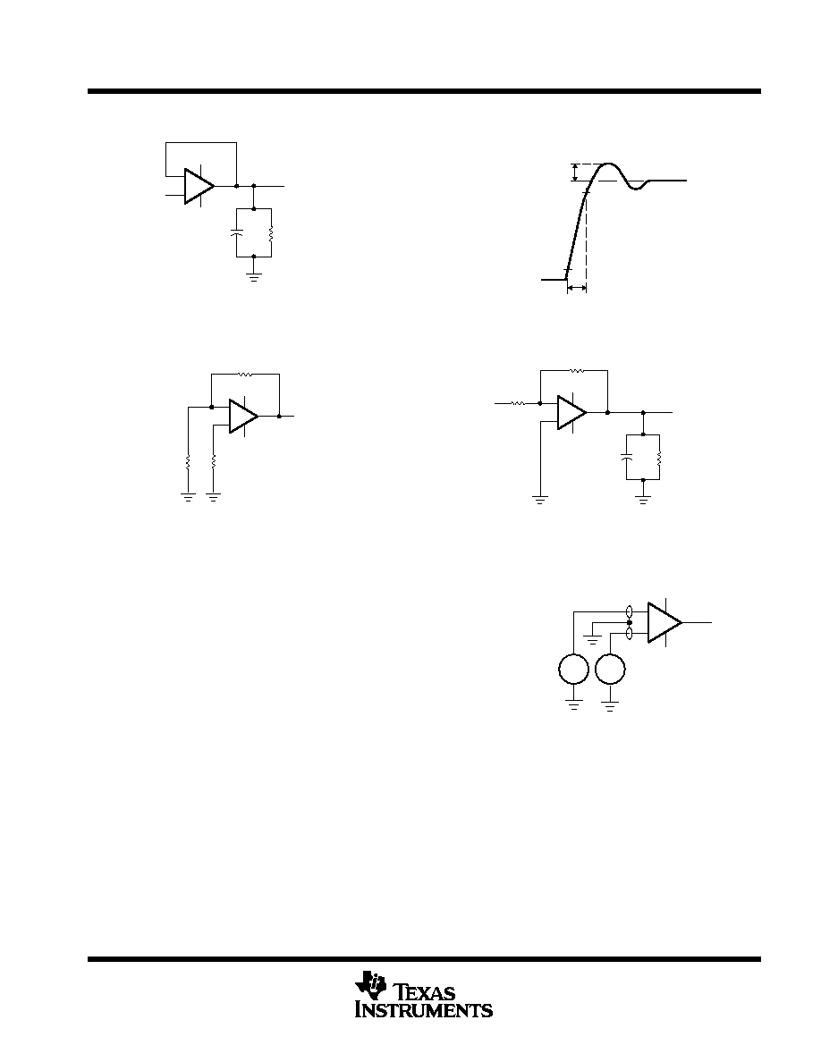
PARAMETER MEASUREMENT INFORMATION
+
≠
VCC+
VCC≠
VI
VO
RL
NOTE A: CL includes fixture capacitance.
CL
(see Note A)
Figure 1. Slew Rate, Rise/Fall Time,
and Overshoot Test Circuit
Overshoot
10%
90%
tr
Figure 2. Rise-Time and Overshoot
Waveform
VCC≠
VCC+
+
≠
VO
RS
RS
2 k
Figure 3. Noise-Voltage Test Circuit
Figure 4. Unity-Gain Bandwidth and
Phase-Margin Test Circuit
VO
VCC≠
VCC+
+
≠
RL
CL
(see Note A)
VI
10 k
100
NOTE A: CL includes fixture capacitance.
typical values
Typical values, as presented in this data sheet
represent the median (50% point) of device
parametric performance.
input bias and offset current
At the picoamp-bias-current level typical of the
TL05x and TL05xA, accurate measurement of the
bias current becomes difficult. Not only does this
measurement require a picoammeter, but
test-socket leakages easily can exceed the actual device bias currents. To accurately measure these small
currents, Texas Instruments uses a two-step process. The socket leakage is measured using picoammeters
with bias voltages applied, but with no device in the socket. The device then is inserted in the socket, and a
second test that measures both the socket leakage and the device input bias current is performed. The two
measurements then are subtracted algebraically to determine the bias current of the device.
noise
Because of the increasing emphasis on low noise levels in many of today's applications, the input noise voltage
density is sample tested at f = 1 kHz. Texas Instruments also has additional noise-testing capability to meet
specific application requirements. Please contact the factory for details.
Figure 5. Input-Bias and Offset-Current Test Circuit
+
≠
VCC+
VCC≠
Ground Shield
pA
pA
TL05x, TL05xA
ENHANCED-JFET LOW-OFFSET
OPERATIONAL AMPLIFIERS
SLOS178A ≠ FEBRUARY 1997 - REVISED FEBRUARY 2003
18
POST OFFICE BOX 655303
∑
DALLAS, TEXAS 75265
TYPICAL CHARACTERISTICS
Table of Graphs
FIGURE
VIO
Input offset voltage
Distribution
6≠11
a
V
IO
Temperature coefficient of input offset voltage
Distribution
12, 13, 14
IIB
Input bias current
vs Common-mode input voltage
vs Free-air temperature
15
16
IIO
Input offset current
vs Free-air temperature
16
VIC
Common-mode input voltage range limits
vs Supply voltage
vs Free-air temperature
17
18
VO
Output voltage
vs Differential input voltage
19, 20
VOM
Maximum peak output voltage
vs Supply voltage
vs Output current
vs Free-air temperature
21
25, 26
27, 28
VO(PP) Maximum peak-to-peak output voltage
vs Frequency
22, 23, 24
AVD
Large-signal differential voltage amplification
vs Load resistance
vs Frequency
vs Free-air temperature
29
30
31, 32, 33
CMRR
Common-mode rejection ratio
vs Frequency
vs Free-air temperature
34, 35
36
zo
Output impedance
vs Frequency
37
kSVR
Supply-voltage rejection ratio
vs Free-air temperature
38
IOS
Short-circuit output current
vs Supply voltage
vs Time
vs Free-air temperature
39
40
41
ICC
Supply current
vs Supply voltage
vs Free-air temperature
42, 43, 44
45, 46, 47
SR
Slew rate
vs Load resistance
vs Free-air temperature
48≠53
54≠59
Overshoot factor
vs Load capacitance
60
Vn
Equivalent input noise voltage
vs Frequency
61, 62
THD
Total harmonic distortion
vs Frequency
63
B1
Unity-gain bandwidth
vs Supply voltage
vs Free-air temperature
64, 65, 66
67, 68, 69
m
Phase margin
vs Supply voltage
vs Load capacitance
vs Free-air temperature
70, 71, 72
73, 74, 75
76, 77, 78
Phase shift
vs Frequency
30
Voltage-follower small-signal pulse response
vs Time
79
Voltage-follower large-signal pulse response
vs Time
80

TL05x, TL05xA
ENHANCED-JFET LOW-OFFSET
OPERATIONAL AMPLIFIERS
SLOS178A ≠ FEBRUARY 1997 - REVISED FEBRUARY 2003
19
POST OFFICE BOX 655303
∑
DALLAS, TEXAS 75265
TYPICAL CHARACTERISTICS
Figure 6
DISTRIBUTION OF TL051
INPUT OFFSET VOLTAGE
8
≠1.5
0
Percentage of Units
≠
%
VIO ≠ Input Offset Voltage ≠ mV
4
12
16
≠0.9
≠0.3
0
0.3
0.9
1.5
433 Units Tested From 1 Wafer Lot
VCC
±
=
±
15 V
TA = 25
∞
C
P Package
≠1.1
≠0.6
0.6
1.1
Figure 7
DISTRIBUTION OF TL051A
INPUT OFFSET VOLTAGE
20
16
12
8
4
900
600
300
0
≠300
≠600
VIO ≠ Input Offset Voltage ≠
µ
V
Percentage of Units
≠
%
0
≠900
ŒŒŒŒŒŒŒŒŒŒ
ŒŒŒŒŒŒŒŒŒŒ
ŒŒŒŒŒŒŒŒŒŒ
393 Units Tested From 1 Wafer Lot
VCC
±
=
±
15 V
TA = 25
∞
C
P Package
Figure 8
≠1.5
0
P
ercen
t
age o
f
A
mp
lifi
ers
≠
%
VIO ≠ Input Offset Voltage ≠ mV
≠0.9
≠0.3
0
0.3
0.9
1.5
3
6
9
12
15
DISTRIBUTION OF TL052
INPUT OFFSET VOLTAGE
476 Amplifiers Tested From 1 Wafer Lot
VCC
±
=
±
15 V
TA = 25
∞
C
P Package
≠1.2
≠0.6
0.6
1.2
Figure 9
0
≠900
≠600
≠300
0
300
600
900
5
10
15
20
VIO ≠ Input Offset Voltage ≠
µ
V
Percentage of
Amplifiers
≠
%
TA = 25
∞
C
DISTRIBUTION OF TL052A
INPUT OFFSET VOLTAGE
403 Amplifiers Tested From 1 Wafer Lot
VCC
±
=
±
15 V
P Package

TL05x, TL05xA
ENHANCED-JFET LOW-OFFSET
OPERATIONAL AMPLIFIERS
SLOS178A ≠ FEBRUARY 1997 - REVISED FEBRUARY 2003
20
POST OFFICE BOX 655303
∑
DALLAS, TEXAS 75265
TYPICAL CHARACTERISTICS
Figure 10
DISTRIBUTION OF TL054
INPUT OFFSET VOLTAGE
15
≠4
0
Percentage of
Amplifiers
≠
%
VIO ≠ Input Offset Voltage ≠ mV
5
25
30
≠2
0
1
3
≠3
≠1
2
4
VCC
±
=
±
15 V
TA = 25
∞
C
N Package
20
10
1140 Amplifiers Tested From 3 Wafer Lots
Figure 11
DISTRIBUTION OF TL054A
INPUT OFFSET VOLTAGE
15
12
9
6
3
1.8
1.2
0.6
0
≠0.6
≠1.2
VIO ≠ Input Offset Voltage ≠ mV
Percentage of
Amplifiers
≠
%
0
≠1.8
1048 Amplifiers Tested From 3 Wafer Lots
VCC
±
=
±
15 V
TA = 25
∞
C
N Package
Figure 12
DISTRIBUTION OF TL051
INPUT OFFSET VOLTAGE
TEMPERATURE COEFFICIENT
≠25
0
Percentage of Units
≠
%
≠ Temperature Coefficient ≠
µ
V/
∞
C
4
8
12
16
20
≠20 ≠15 ≠10
≠5
0
5
10
15
20
25
ŒŒŒŒŒŒŒŒŒŒ
120 Units Tested From 2 Wafer Lots
VCC
±
=
±
15 V
TA = 25
∞
C to 125
∞
C
P Package
a
V
IO
0
Percentage of
Amplifiers
≠
%
≠ Temperature Coefficient ≠
µ
V/
∞
C
20
30
5
10
15
20
10
0
≠10
≠20
≠30
DISTRIBUTION OF TL052
INPUT OFFSET VOLTAGE
TEMPERATURE COEFFICIENT
ŒŒŒŒŒŒŒŒŒŒŒ
ŒŒŒŒŒŒŒŒŒŒŒ
172 Amplifiers Tested From 2 Wafer Lots
VCC
±
=
±
15 V
TA = 25
∞
C to 125
∞
C
P Package
ŒŒŒŒŒŒŒŒŒŒ
Outlier: One Unit at ≠34.6
µ
V/
∞
C
Figure 13
a
V
IO

TL05x, TL05xA
ENHANCED-JFET LOW-OFFSET
OPERATIONAL AMPLIFIERS
SLOS178A ≠ FEBRUARY 1997 - REVISED FEBRUARY 2003
21
POST OFFICE BOX 655303
∑
DALLAS, TEXAS 75265
TYPICAL CHARACTERISTICS
Figure 14
DISTRIBUTION OF TL054
INPUT OFFSET VOLTAGE
TEMPERATURE COEFFICIENT
≠60
0
≠ Temperature Coefficient ≠
µ
V/
∞
C
30
40
50
≠40
≠20
0
20
40
60
ŒŒŒŒŒŒŒŒŒŒŒŒ
ŒŒŒŒŒŒŒŒŒŒŒŒ
324 Amplifiers Tested From 3 Wafer Lots
VCC
±
=
±
15 V
TA = 25
∞
C to 125
∞
C
N Package
20
10
Percentage of
Amplifiers
≠
%
a
V
IO
Figure 15
≠15
≠10
≠
Input Bias Current
≠
nA
VIC ≠ Common-Mode Input Voltage ≠ V
≠5
0
5
10
≠10
≠5
0
5
10
15
TA = 25
∞
C
VCC
±
=
±
15 V
INPUT BIAS CURRENT
vs
COMMON-MODE INPUT VOLTAGE
I
IB
Figure 16
INPUT BIAS CURRENT AND
INPUT OFFSET CURRENT
vs
FREE-AIR TEMPERATURE
IIO
IIB
TA ≠ Free-Air Temperature ≠
∞
C
≠
Input Bias and Offset Currents
≠
nA
0.001
25
0.01
0.1
1
10
100
45
65
85
105
125
VCC
±
=
±
15 V
VO = 0
VIC = 0
I
IB
and
I
IO
Figure 17
0
≠16
≠
Common-Mode Input V
oltage
≠
V
|VCC
±
| ≠ Supply Voltage ≠ V
≠12
≠8
≠4
0
4
8
12
16
2
4
6
8
10
12
14
16
TA = 25
∞
C
COMMON-MODE
INPUT VOLTAGE RANGE LIMITS
vs
SUPPLY VOLTAGE
V
IC
ŒŒŒŒŒ
Negative Limit
ŒŒŒŒŒ
Positive Limit
Data at high and low temperatures are applicable only within the rated operating free-air temperature ranges of the various devices.

TL05x, TL05xA
ENHANCED-JFET LOW-OFFSET
OPERATIONAL AMPLIFIERS
SLOS178A ≠ FEBRUARY 1997 - REVISED FEBRUARY 2003
22
POST OFFICE BOX 655303
∑
DALLAS, TEXAS 75265
TYPICAL CHARACTERISTICS
Figure 18
≠75
≠20
TA ≠ Free-Air Temperature ≠
∞
C
≠15
≠10
≠5
0
5
10
15
20
≠50
≠25
0
25
50
75
100
125
COMMON-MODE
INPUT VOLTAGE RANGE LIMITS
vs
FREE-AIR TEMPERATURE
≠
Common-Mode Input V
oltage
≠
V
V
IC
ŒŒŒŒŒ
ŒŒŒŒŒ
VCC
±
=
±
15 V
ŒŒŒŒŒ
ŒŒŒŒŒ
Positive Limit
ŒŒŒŒŒ
ŒŒŒŒŒ
Negative Limit
Figure 19
≠200
≠5
≠
Output V
oltage
≠
V
≠4
≠3
≠2
≠1
0
1
2
3
4
5
≠100
0
100
200
ŒŒŒŒ
ŒŒŒŒ
TA = 25
∞
C
OUTPUT VOLTAGE
vs
DIFFERENTIAL INPUT VOLTAGE
VID ≠ Differential Input Voltage ≠
µ
V
V
O
ŒŒŒŒ
ŒŒŒŒ
RL = 600
ŒŒŒŒ
ŒŒŒŒ
RL = 1 k
ŒŒŒŒŒ
RL = 10 k
ŒŒŒŒŒ
ŒŒŒŒŒ
RL = 2 k
ŒŒŒŒŒ
VCC
±
=
±
5 V
Figure 20
≠400
≠15
VID ≠ Differential Input Voltage ≠
µ
V
≠10
≠5
0
5
10
15
≠200
0
200
400
OUTPUT VOLTAGE
vs
DIFFERENTIAL INPUT VOLTAGE
≠
Output V
oltage
≠
V
V
O
¡¡¡¡
¡¡¡¡
¡¡¡¡
¡¡¡¡
ŒŒŒŒ
RL = 600
ŒŒŒŒ
ŒŒŒŒ
RL = 1 k
ŒŒŒŒ
RL = 2 k
ŒŒŒŒ
RL = 10 k
ŒŒŒŒŒ
ŒŒŒŒŒ
VCC
±
=
±
15 V
ŒŒŒŒ
TA = 25
∞
C
Figure 21
0
≠8
≠
Maximum Peak Output V
oltage
≠
V
|VCC
±
| ≠ Supply Voltage ≠ V
≠4
0
4
8
12
16
2
4
6
8
10
12
14
16
TA = 25
∞
C
VOM+
RL = 10 k
RL = 2 k
VOM≠
RL = 2 k
RL = 10 k
MAXIMUM PEAK OUTPUT VOLTAGE
vs
SUPPLY VOLTAGE
≠12
≠16
V
OM
Data at high and low temperatures are applicable only within the rated operating free-air temperature ranges of the various devices.
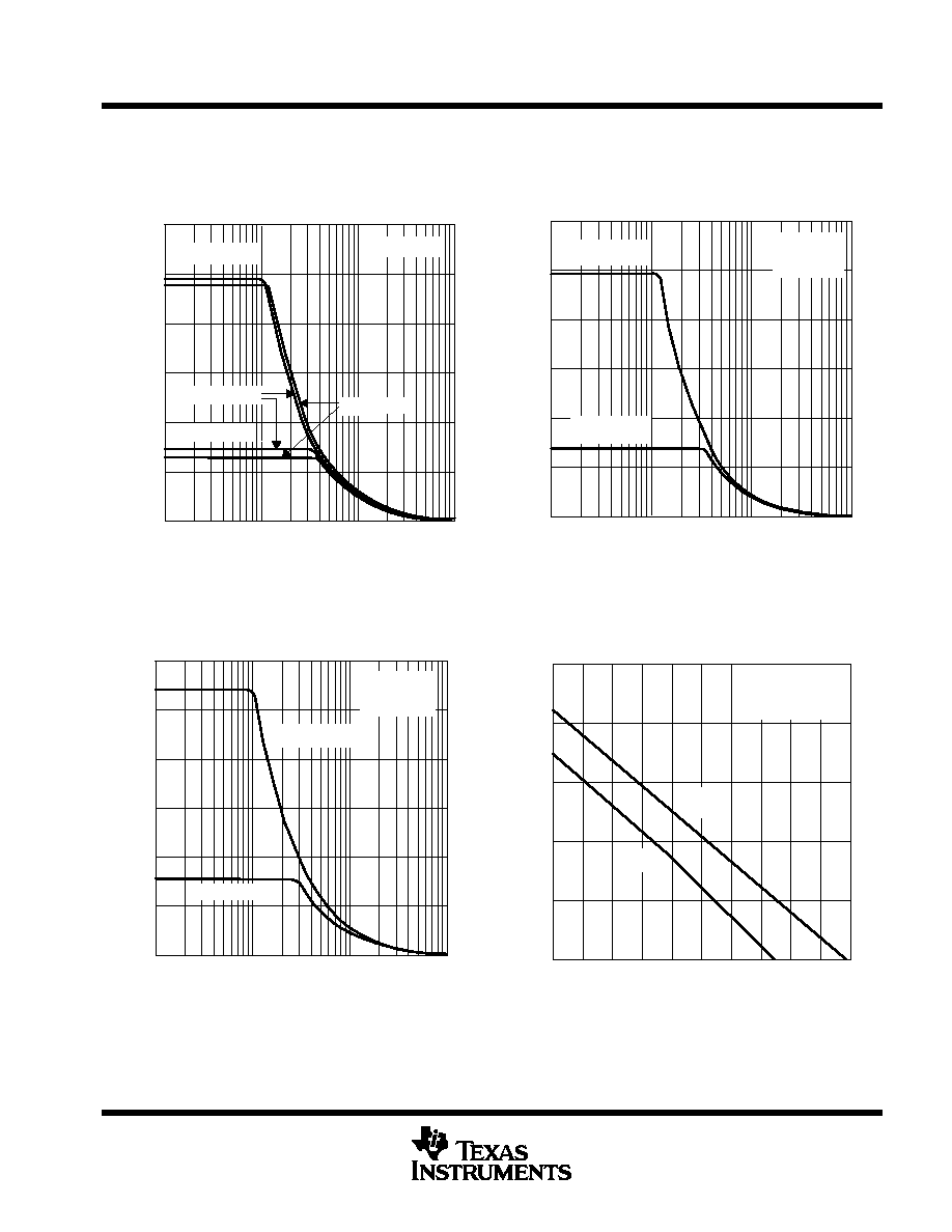
TL05x, TL05xA
ENHANCED-JFET LOW-OFFSET
OPERATIONAL AMPLIFIERS
SLOS178A ≠ FEBRUARY 1997 - REVISED FEBRUARY 2003
23
POST OFFICE BOX 655303
∑
DALLAS, TEXAS 75265
TYPICAL CHARACTERISTICS
Figure 22
0
10 k
f ≠ Frequency ≠ Hz
5
10
15
20
25
30
100 k
1 M
10 M
≠
Maximum Peak-to-Peak Output V
oltage
≠
V
RL = 2 k
TA = 125
∞
C
VCC
±
=
±
5 V
TA = ≠55
∞
C
VCC
±
=
±
15 V
MAXIMUM PEAK-TO-PEAK OUTPUT VOLTAGE
vs
FREQUENCY
V
O(PP)
Figure 23
≠
Maximum Peak-to-Peak Output V
oltage
≠
V
0
10 k
f ≠ Frequency ≠ Hz
5
10
15
20
25
30
100 k
1 M
10 M
MAXIMUM PEAK-TO-PEAK OUTPUT VOLTAGE
vs
FREQUENCY
V
O(PP)
¡¡¡¡
¡¡¡¡
¡¡¡¡
TA = 25
∞
C
RL = 2 k
¡¡¡¡¡
¡¡¡¡¡
VCC
±
=
±
5 V
¡¡¡¡¡
¡¡¡¡¡
VCC
±
=
±
15 V
Figure 24
20
25
30
15
10
5
0
10 k
100 k
f ≠ Frequency ≠ Hz
1 M
10 M
MAXIMUM PEAK-TO-PEAK OUTPUT VOLTAGE
vs
FREQUENCY
≠
Maximum Peak-to-Peak Output V
oltage
≠
V
V
O(PP)
¡¡¡¡
¡¡¡¡
RL = 10 k
TA = 25
∞
C
¡¡¡¡¡
¡¡¡¡¡
VCC
±
=
±
15 V
¡¡¡¡¡
¡¡¡¡¡
VCC
±
=
±
5 V
Figure 25
0
0
≠
Maximum Peak Output V
oltage
≠
V
|IO| ≠ Output Current ≠ mA
1
2
3
4
5
4
12
16
20
8
MAXIMUM PEAK OUTPUT VOLTAGE
vs
OUTPUT CURRENT
|V
OM
|
¡¡¡¡¡
¡¡¡¡¡
¡¡¡¡¡
¡¡¡¡¡
¡¡¡
¡¡¡
VOM≠
¡¡¡
¡¡¡
VOM+
VCC
±
=
±
5 V
RL = 10 k
TA = 25
∞
C
2
6
10
14
18
Data at high and low temperatures are applicable only within the rated operating free-air temperature ranges of the various devices.

TL05x, TL05xA
ENHANCED-JFET LOW-OFFSET
OPERATIONAL AMPLIFIERS
SLOS178A ≠ FEBRUARY 1997 - REVISED FEBRUARY 2003
24
POST OFFICE BOX 655303
∑
DALLAS, TEXAS 75265
TYPICAL CHARACTERISTICS
Figure 26
0
0
2
4
6
8
10
12
14
16
10
20
30
40
50
|IO| ≠ Output Current ≠ mA
MAXIMUM PEAK OUTPUT VOLTAGE
vs
OUTPUT CURRENT
≠
Maximum Peak Output V
oltage
≠
V
|V
OM
|
¡¡¡¡¡
¡¡¡¡¡
¡¡¡¡¡
¡¡¡¡¡
VCC
±
=
±
15 V
RL = 10 k
TA = 25
∞
C
¡¡¡
¡¡¡
VOM≠
¡¡¡¡
¡¡¡¡
VOM+
5
15
25
35
45
Figure 27
≠75
≠5
TA ≠ Free-Air Temperature ≠
∞
C
≠4
≠3
≠2
≠1
0
1
2
3
4
5
≠50
≠25
0
25
50
75
100
125
RL = 2 k
RL = 10 k
RL = 10 k
RL = 2 k
VOM+
VCC
±
=
±
5 V
MAXIMUM PEAK OUTPUT VOLTAGE
vs
FREE-AIR TEMPERATURE
≠
Maximum Peak Output V
oltage
≠
V
V
OM
¡¡¡
¡¡¡
VOM≠
Figure 28
≠75
≠16
≠50
≠25
0
25
50
75
100
125
≠12
≠8
≠4
0
4
8
12
16
TA ≠ Free-Air Temperature ≠
∞
C
RL = 10 k
RL = 10 k
RL = 2 k
RL = 2 k
VCC
±
=
±
15 V
MAXIMUM PEAK OUTPUT VOLTAGE
vs
FREE-AIR TEMPERATURE
≠
Maximum Peak Output V
oltage
≠
V
V
OM
¡¡¡
¡¡¡
VOM+
¡¡¡
¡¡¡
VOM≠
Figure 29
≠
Differential V
oltage
Amplification
≠
V/mV
0.4
0
RL ≠ Load Resistance ≠ k
50
100
150
200
250
1
4
10
40
100
VO =
±
1 V
TA = 25
∞
C
VCC
±
=
±
15 V
LARGE-SIGNAL DIFFERENTIAL VOLTAGE
AMPLIFICATION
vs
LOAD RESISTANCE
VCC
±
=
±
5 V
A
VD
Data at high and low temperatures are applicable only within the rated operating free-air temperature ranges of the various devices.

TL05x, TL05xA
ENHANCED-JFET LOW-OFFSET
OPERATIONAL AMPLIFIERS
SLOS178A ≠ FEBRUARY 1997 - REVISED FEBRUARY 2003
25
POST OFFICE BOX 655303
∑
DALLAS, TEXAS 75265
TYPICAL CHARACTERISTICS
10
f ≠ Frequency ≠ Hz
10 M
100
1 k
10 k
100 k
1 M
0.1
1
101
104
102
103
VCC
±
=
±
15 V
RL = 2 k
CL = 25 pF
TA = 25
∞
C
AVD
Phase Shift
0
∞
30
∞
60
∞
90
∞
120
∞
150
∞
180
∞
LARGE-SIGNAL DIFFERENTIAL VOLTAGE
AMPLIFICATION AND PHASE SHIFT
vs
FREQUENCY
106
105
≠
Differential V
oltage
Amplification
≠
V/mV
A
VD
m
≠
Phase Shift
Figure 30
≠75
10
TA ≠ Free-Air Temperature ≠
∞
C
125
1000
≠50
≠25
0
25
50
75
100
40
100
400
RL = 2 k
RL = 10 k
VCC
±
=
±
5 V
VO =
±
2.3 V
≠
Differential V
oltage
Amplification
≠
V/mV
A
VD
Figure 31
TL051 AND TL052
LARGE-SIGNAL DIFFERENTIAL
VOLTAGE AMPLIFICATION
vs
FREE-AIR TEMPERATURE
Figure 32
≠75
10
TA ≠ Free-Air Temperature ≠
∞
C
125
1000
≠50
≠25
0
25
50
75
100
40
100
400
RL = 2 k
RL = 10 k
VCC
±
=
±
5 V
VO =
±
2.3 V
≠
Differential V
oltage
Amplification
≠
V/mV
A
VD
TL054
LARGE-SIGNAL DIFFERENTIAL
VOLTAGE AMPLIFICATION
vs
FREE-AIR TEMPERATURE
Data at high and low temperatures are applicable only within the rated operating free-air temperature ranges of the various devices.

TL05x, TL05xA
ENHANCED-JFET LOW-OFFSET
OPERATIONAL AMPLIFIERS
SLOS178A ≠ FEBRUARY 1997 - REVISED FEBRUARY 2003
26
POST OFFICE BOX 655303
∑
DALLAS, TEXAS 75265
TYPICAL CHARACTERISTICS
Figure 33
≠75
10
125
1000
≠50
≠25
0
25
50
75
100
40
100
400
RL = 10 k
RL = 2 k
TA ≠ Free-Air Temperature ≠
∞
C
LARGE-SIGNAL DIFFERENTIAL VOLTAGE
AMPLIFICATION
vs
FREE-AIR TEMPERATURE
¡¡¡¡¡
¡¡¡¡¡
VCC
±
=
±
15 V
VO = 10 V
≠
Differential V
oltage
Amplification
≠
V/mV
A
VD
Figure 34
10
0
CMRR
≠
Common-Mode Rejection Ratio
≠
dB
f ≠ Frequency ≠ Hz
10 M
100
100
1 k
10 k
100 k
1 M
10
20
30
40
50
60
70
80
90
VCC
±
=
±
5 V
TA = 25
∞
C
COMMON-MODE REJECTION RATIO
vs
FREQUENCY
Figure 35
90
80
70
60
50
40
30
20
10
100
0
1 M
100 k
10 k
1 k
100
10 M
f ≠ Frequency ≠ Hz
10
VCC
±
=
±
15 V
TA = 25
∞
C
COMMON-MODE REJECTION RATIO
vs
FREQUENCY
CMRR
≠
Common-Mode Rejection Ratio
≠
dB
Figure 36
≠75
70
TA ≠ Free-Air Temperature ≠
∞
C
100
75
80
85
90
95
≠50
≠25
0
25
50
75
100
VIC = VICRMin
VCC
±
=
±
5 V
VCC
±
=
±
15 V
COMMON-MODE REJECTION RATIO
vs
FREE-AIR TEMPERATURE
CMRR
≠
Common-Mode Rejection Ratio
≠
dB
125
Data at high and low temperatures are applicable only within the rated operating free-air temperature ranges of the various devices.

TL05x, TL05xA
ENHANCED-JFET LOW-OFFSET
OPERATIONAL AMPLIFIERS
SLOS178A ≠ FEBRUARY 1997 - REVISED FEBRUARY 2003
27
POST OFFICE BOX 655303
∑
DALLAS, TEXAS 75265
TYPICAL CHARACTERISTICS
Figure 37
1 k
0.1
≠
Output Impedance
≠
1 M
100
10 k
100 k
1
10
f ≠ Frequency ≠ Hz
AVD = 100
AVD = 10
AVD = 1
VCC
±
=
±
15 V
TA = 25
∞
C
ro (open loop)
250
OUTPUT IMPEDANCE
vs
FREQUENCY
z o
0.4
4
40
Figure 38
≠75
90
kSVR
≠
Supply-V
oltage Rejection Ratio
≠
dB
TA ≠ Free-Air Temperature ≠
∞
C
125
≠50
≠25
0
25
50
75
100
94
98
VCC
±
=
±
5 V to
±
15 V
SUPPLY-VOLTAGE REJECTION RATIO
vs
FREE-AIR TEMPERATURE
110
106
102
¡¡
¡¡
¡¡
k
SVR
Figure 39
0
IOS
≠
Short-Circuit Output Current
≠
mA
|VCC
±
| ≠ Supply Voltage ≠ V
16
60
2
4
6
8
10
12
14
0
20
40
VO = 0
TA = 25
∞
C
VID = 100 mV
VID = ≠100 mV
SHORT-CIRCUIT OUTPUT CURRENT
vs
SUPPLY VOLTAGE
≠20
≠40
≠60
¡¡
¡¡
I OS
Figure 40
0
t ≠ Time ≠ s
40
20
≠20
≠40
60
≠60
50
40
30
20
10
60
0
TA = 25
∞
C
VCC
±
=
±
15 V
VID = 100 mV
VID = ≠100 mV
SHORT-CIRCUIT OUTPUT CURRENT
vs
TIME
IOS
≠
Short-Circuit Output Current
≠
mA
¡¡
¡¡
¡¡
I OS
Data at high and low temperatures are applicable only within the rated operating free-air temperature ranges of the various devices.

TL05x, TL05xA
ENHANCED-JFET LOW-OFFSET
OPERATIONAL AMPLIFIERS
SLOS178A ≠ FEBRUARY 1997 - REVISED FEBRUARY 2003
28
POST OFFICE BOX 655303
∑
DALLAS, TEXAS 75265
TYPICAL CHARACTERISTICS
Figure 41
VO = 0
0
TA ≠ Free-Air Temperature ≠
∞
C
40
20
≠20
≠40
60
≠60
100
75
50
25
0
≠25
≠50
125
≠75
VCC
±
=
±
15 V
VCC
±
=
±
5 V
VCC
±
=
±
5 V
VCC
±
=
±
15 V
SHORT-CIRCUIT OUTPUT CURRENT
vs
FREE-AIR TEMPERATURE
IOS
≠
Short-Circuit Output Current
≠
mA
¡¡
¡¡
I OS
ŒŒŒŒŒ
ŒŒŒŒŒ
VID = 100 m V
ŒŒŒŒŒŒ
VID = ≠100 m V
Figure 42
0
0
|VCC
±
| ≠ Supply Voltage ≠ V
16
3
2
4
6
8
10
12
14
0.5
1
1.5
2
2.5
TA = 25
∞
C
TA = ≠55
∞
C
TA = 125
∞
C
VO = 0
No Load
ICC
≠
Supply Current
≠
mA
¡¡
¡¡
¡¡
I CC
TL051
SUPPLY CURRENT
vs
SUPPLY VOLTAGE
0
0
5
2
4
6
8
10
12
14
1
2
3
4
TA = 25
∞
C
TA = ≠55
∞
C
TA = 125
∞
C
VO = 0
No Load
16
ICC
≠
Supply Current
≠
mA
¡¡
¡¡
¡¡
I CC
|VCC
±
| ≠ Supply Voltage ≠ V
Figure 43
TL052
SUPPLY CURRENT
vs
SUPPLY VOLTAGE
Figure 44
0
0
|VCC
±
| ≠ Supply Voltage ≠ V
16
10
2
4
6
8
10
12
14
2
4
6
8
TA = 25
∞
C
ŒŒŒŒŒ
ŒŒŒŒŒ
TA = ≠55
∞
C
TA = 125
∞
C
VO = 0
No Load
ICC
≠
Supply Current
≠
mA
¡¡
¡¡
I CC
TL054
SUPPLY CURRENT
vs
SUPPLY VOLTAGE
Data at high and low temperatures are applicable only within the rated operating free-air temperature ranges of the various devices.
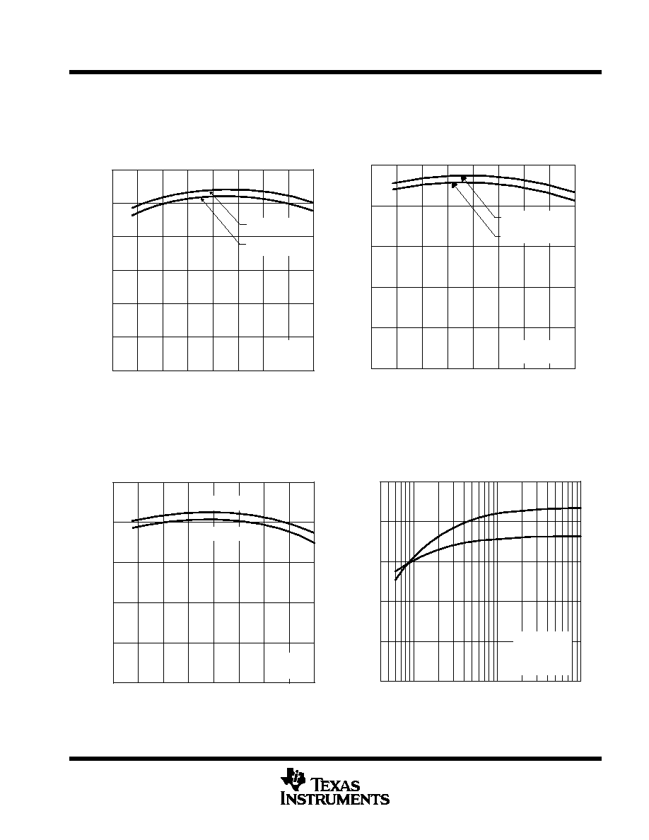
TL05x, TL05xA
ENHANCED-JFET LOW-OFFSET
OPERATIONAL AMPLIFIERS
SLOS178A ≠ FEBRUARY 1997 - REVISED FEBRUARY 2003
29
POST OFFICE BOX 655303
∑
DALLAS, TEXAS 75265
TYPICAL CHARACTERISTICS
Figure 45
≠75
0
125
3
≠50
≠25
0
25
50
75
100
0.5
1
1.5
2
2.5
TA ≠ Free-Air Temperature ≠
∞
C
VCC
±
=
±
5 V
VCC
±
=
±
15 V
VO = 0
No Load
ICC
≠
Supply Current
≠
mA
¡¡
¡¡
I CC
TL051
SUPPLY CURRENT
vs
FREE-AIR TEMPERATURE
Figure 46
≠75
0
125
5
≠50
≠25
0
25
50
75
100
1
2
3
4
VCC
±
=
±
15 V
VCC
±
=
±
5 V
ICC
≠
Supply Current
≠
mA
¡¡
¡¡
¡¡
I CC
TA ≠ Free-Air Temperature ≠
∞
C
VO = 0
No Load
TL052
SUPPLY CURRENT
vs
FREE-AIR TEMPERATURE
Figure 47
≠75
0
125
10
≠50
≠25
0
25
50
75
100
2
4
6
8
TA ≠ Free-Air Temperature ≠
∞
C
ICC
≠
Supply Current
≠
mA
¡¡
¡¡
¡¡
I CC
ŒŒŒŒŒŒ
ŒŒŒŒŒŒ
VCC
±
=
±
5 V
ŒŒŒŒŒŒ
ŒŒŒŒŒŒ
VCC
±
=
±
15 V
VO = 0
No Load
TL054
SUPPLY CURRENT
vs
FREE-AIR TEMPERATURE
Figure 48
25
20
15
10
SR
≠
Slew Rate
≠
V/
5
0
100
40
10
4
1
RL ≠ Load Resistance ≠ k
0.4
SR+
SR≠
CL = 100 pF
TA = 25
∞
C
See Figure 1
VCC
±
=
±
5 V
µ
s
TL051
SLEW RATE
vs
LOAD RESISTANCE
Data at high and low temperatures are applicable only within the rated operating free-air temperature ranges of the various devices.
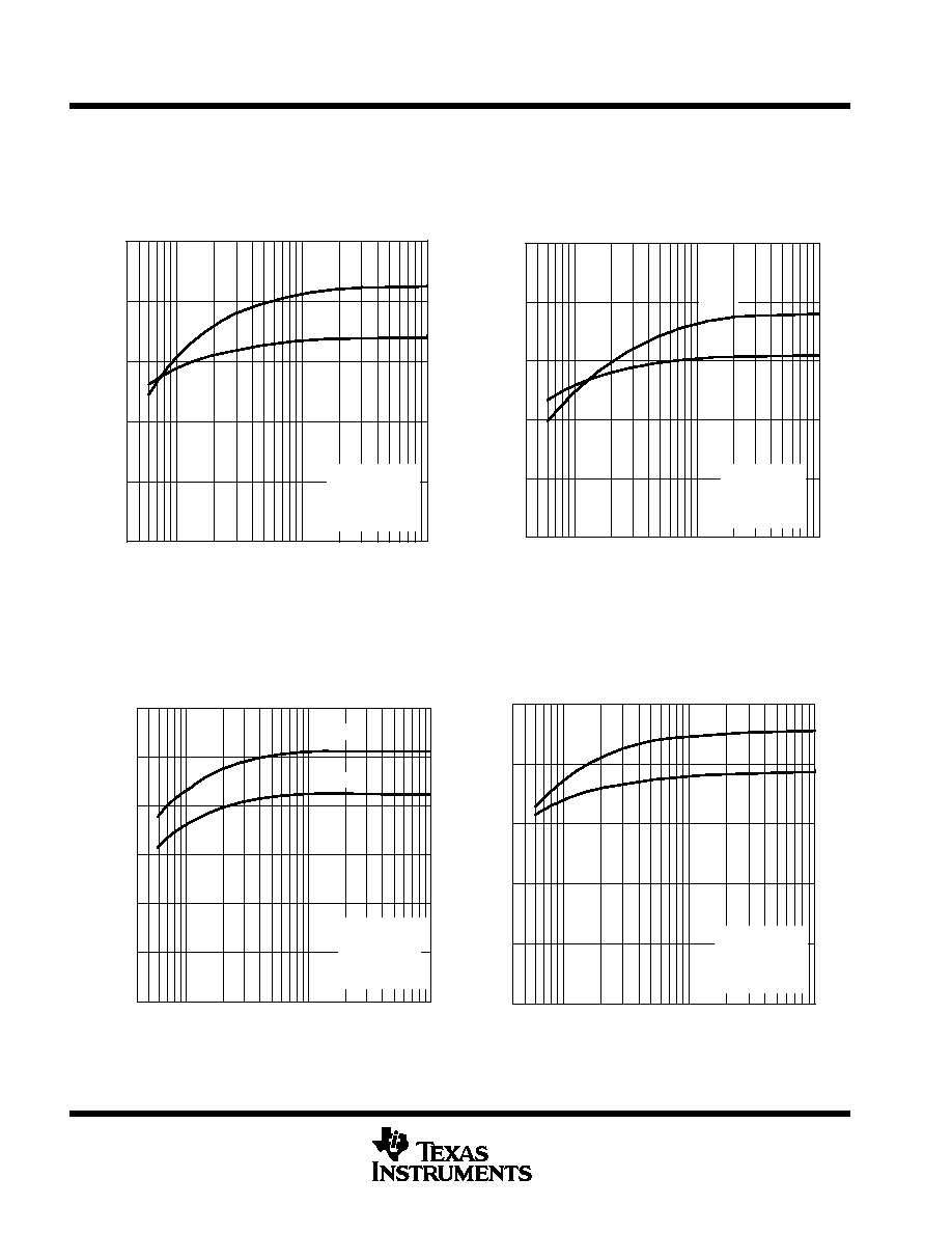
TL05x, TL05xA
ENHANCED-JFET LOW-OFFSET
OPERATIONAL AMPLIFIERS
SLOS178A ≠ FEBRUARY 1997 - REVISED FEBRUARY 2003
30
POST OFFICE BOX 655303
∑
DALLAS, TEXAS 75265
TYPICAL CHARACTERISTICS
10
4
1
0.4
0
RL ≠ Load Resistance ≠ k
25
5
10
15
20
SR≠
SR+
40
CL = 100 pF
TA = 25
∞
C
See Figure 1
VCC
±
=
±
5 V
SR
≠
Slew Rate
≠
V/
µ
s
Figure 49
TL052
SLEW RATE
vs
LOAD RESISTANCE
100
Figure 50
25
20
15
10
SR
≠
Slew Rate
≠
V/
5
0
100
40
10
4
1
RL ≠ Load Resistance ≠ k
0.4
ŒŒ
SR+
SR≠
CL = 100 pF
TA = 25
∞
C
See Figure 1
VCC
±
=
±
5 V
µ
s
TL054
SLEW RATE
vs
LOAD RESISTANCE
Figure 51
25
0
0.4
RL ≠ Load Resistance ≠ k
5
10
15
20
30
1
4
10
40
100
SR+
SR≠
SR
≠
Slew Rate
≠
V/
µ
s
CL = 100 pF
TA = 25
∞
C
See Figure 1
VCC
±
=
±
15 V
TL051
SLEW RATE
vs
LOAD RESISTANCE
1
4
10
40
100
0.4
RL ≠ Load Resistance ≠ k
SR+
SR≠
CL = 100 pF
TA = 25
∞
C
See Figure 1
VCC
±
=
±
15 V
SR
≠
Slew Rate
≠
V/
µ
s
0
25
5
10
15
20
Figure 52
TL052
SLEW RATE
vs
LOAD RESISTANCE
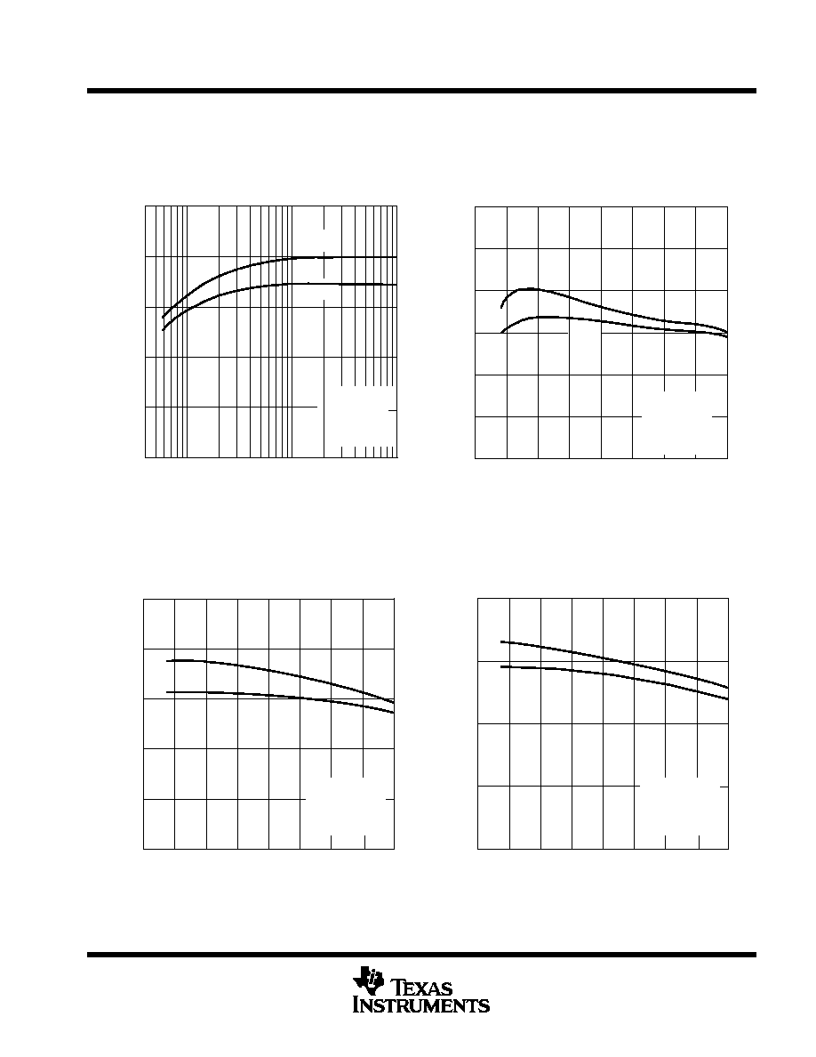
TL05x, TL05xA
ENHANCED-JFET LOW-OFFSET
OPERATIONAL AMPLIFIERS
SLOS178A ≠ FEBRUARY 1997 - REVISED FEBRUARY 2003
31
POST OFFICE BOX 655303
∑
DALLAS, TEXAS 75265
TYPICAL CHARACTERISTICS
Figure 53
20
0
0.4
RL ≠ Load Resistance ≠ k
5
10
15
25
1
4
10
40
100
SR+
SR≠
SR
≠
Slew Rate
≠
V/
µ
s
CL = 100 pF
TA = 25
∞
C
See Figure 1
VCC
±
=
±
5 V
TL054
SLEW RATE
vs
LOAD RESISTANCE
Figure 54
≠75
0
TA ≠ Free-Air Temperature ≠
∞
C
125
30
≠50
≠25
0
25
50
75
100
5
10
15
20
25
VCC
±
=
±
5 V
RL = 2 k
SR+
SR≠
SR
≠
Slew Rate
≠
V/
µ
s
TL051
SLEW RATE
vs
FREE-AIR TEMPERATURE
Figure 55
SR+
SR≠
≠75
0
TA ≠ Free-Air Temperature ≠
∞
C
125
≠50
≠25
0
25
50
75
100
5
10
15
20
25
VCC
±
=
±
5 V
RL = 2 k
CL = 100 pF
See Figure 1
SR
≠
Slew Rate
≠
V/
µ
s
TL052
SLEW RATE
vs
FREE-AIR TEMPERATURE
Figure 56
SR+
SR≠
≠75
0
TA ≠ Free-Air Temperature ≠
∞
C
125
≠50
≠25
0
25
50
75
100
5
10
15
20
VCC
±
=
±
5 V
RL = 2 k
CL = 100 pF
See Figure 1
SR
≠
Slew Rate
≠
V/
µ
s
TL054
SLEW RATE
vs
FREE-AIR TEMPERATURE
Data at high and low temperatures are applicable only within the rated operating free-air temperature ranges of the various devices.

TL05x, TL05xA
ENHANCED-JFET LOW-OFFSET
OPERATIONAL AMPLIFIERS
SLOS178A ≠ FEBRUARY 1997 - REVISED FEBRUARY 2003
32
POST OFFICE BOX 655303
∑
DALLAS, TEXAS 75265
TYPICAL CHARACTERISTICS
Figure 57
≠75
0
TA ≠ Free-Air Temperature ≠
∞
C
125
30
≠50
≠25
0
25
50
75
100
5
10
15
20
25
VCC
±
=
±
15 V
RL = 2 k
CL = 100 pF
See Figure 1
SR≠
SR+
SR
≠
Slew Rate
≠
V/
µ
s
TL051
SLEW RATE
vs
FREE-AIR TEMPERATURE
SR≠
SR+
≠75
0
TA ≠ Free-Air Temperature ≠
∞
C
125
≠50
≠25
0
25
50
75
100
5
10
15
20
25
VCC
±
=
±
15 V
RL = 2 k
CL = 100 pF
See Figure 1
SR
≠
Slew Rate
≠
V/
µ
s
Figure 58
TL052
SLEW RATE
vs
FREE-AIR TEMPERATURE
Figure 59
SR≠
SR+
≠75
0
TA ≠ Free-Air Temperature ≠
∞
C
125
≠50
≠25
0
25
50
75
100
5
10
15
20
VCC
±
=
±
15 V
RL = 2 k
CL = 100 pF
See Figure 1
SR
≠
Slew Rate
≠
V/
µ
s
TL054
SLEW RATE
vs
FREE-AIR TEMPERATURE
Figure 60
ŒŒŒŒŒ
ŒŒŒŒŒ
See Figure 1
ŒŒŒŒŒ
TA = 25
∞
C
ŒŒŒŒŒ
RL = 2 k
ŒŒŒŒŒ
ŒŒŒŒŒ
VI(PP) =
±
10 mV
0
0
Overshoot Factor
≠
%
CL ≠ Load Capacitance ≠ pF
300
50
50
100
150
200
250
10
20
30
40
OVERSHOOT FACTOR
vs
LOAD CAPACITANCE
ŒŒŒŒŒ
VCC
±
=
±
15 V
ŒŒŒŒ
ŒŒŒŒ
VCC
±
=
±
5 V
Data at high and low temperatures are applicable only within the rated operating free-air temperature ranges of the various devices.
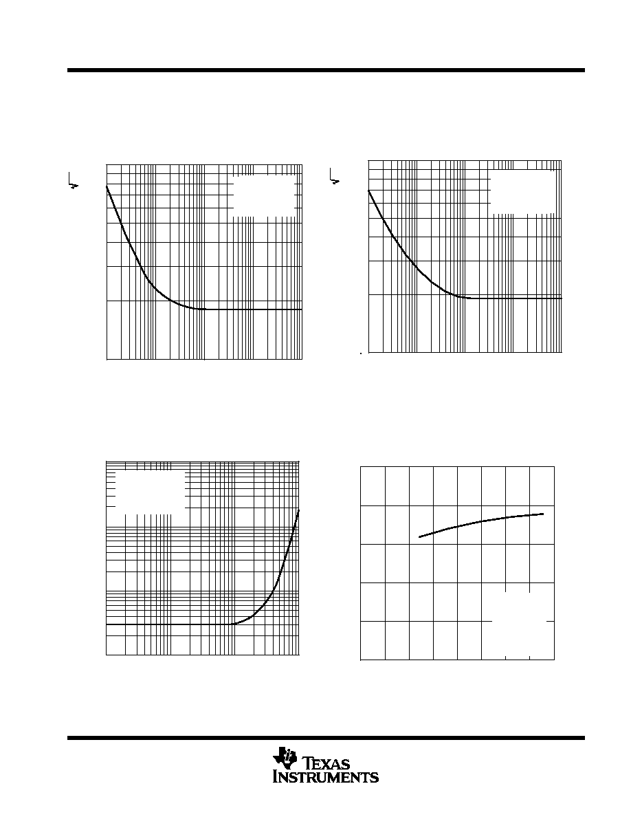
TL05x, TL05xA
ENHANCED-JFET LOW-OFFSET
OPERATIONAL AMPLIFIERS
SLOS178A ≠ FEBRUARY 1997 - REVISED FEBRUARY 2003
33
POST OFFICE BOX 655303
∑
DALLAS, TEXAS 75265
TYPICAL CHARACTERISTICS
Figure 61
f ≠ Frequency ≠ Hz
10
Vn
≠
Equivalent Input Noise V
oltage
≠
10
20
30
40
50
70
100
100
1 k
10 k
100 k
VCC
±
=
±
15 V
RS = 20
TA = 25
∞
C
See Figure 3
nV/
Hz
TL051
EQUIVALENT INPUT NOISE VOLTAGE
vs
FREQUENCY
f ≠ Frequency ≠ Hz
10
Vn
≠
Equivalent Input Noise V
oltage
≠
10
20
30
40
50
70
100
100
1 k
10 k
100 k
nV/
Hz
¡¡¡¡¡
¡¡¡¡¡
¡¡¡¡¡
¡¡¡¡¡
VCC
±
=
±
15 V
RS = 20
TA = 25
∞
C
See Figure 3
Figure 62
TL052 AND TL054
EQUIVALENT INPUT NOISE VOLTAGE
vs
FREQUENCY
VO(RMS) = 6 V
0.001
100
f ≠ Frequency ≠ Hz
THD
≠
T
otal Harmonic Distortion
≠
%
0.01
0.1
1
1 k
10 k
100 k
VCC
±
=
±
15 V
AVD = 1
TA = 25
∞
C
TOTAL HARMONIC DISTORTION
vs
FREQUENCY
0.004
0.04
0.4
Figure 63
Figure 64
0
2.7
≠
Unity-Gain Bandwidth
≠
MHz
|VCC
±
| ≠ Supply Voltage ≠ V
16
3.2
2
4
6
8
10
12
14
2.8
2.9
3
3.1
VI = 10 mV
RL = 2 k
CL = 25 pF
TA = 25
∞
C
See Figure 4
B
1
TL051
UNITY-GAIN BANDWIDTH
vs
SUPPLY VOLTAGE
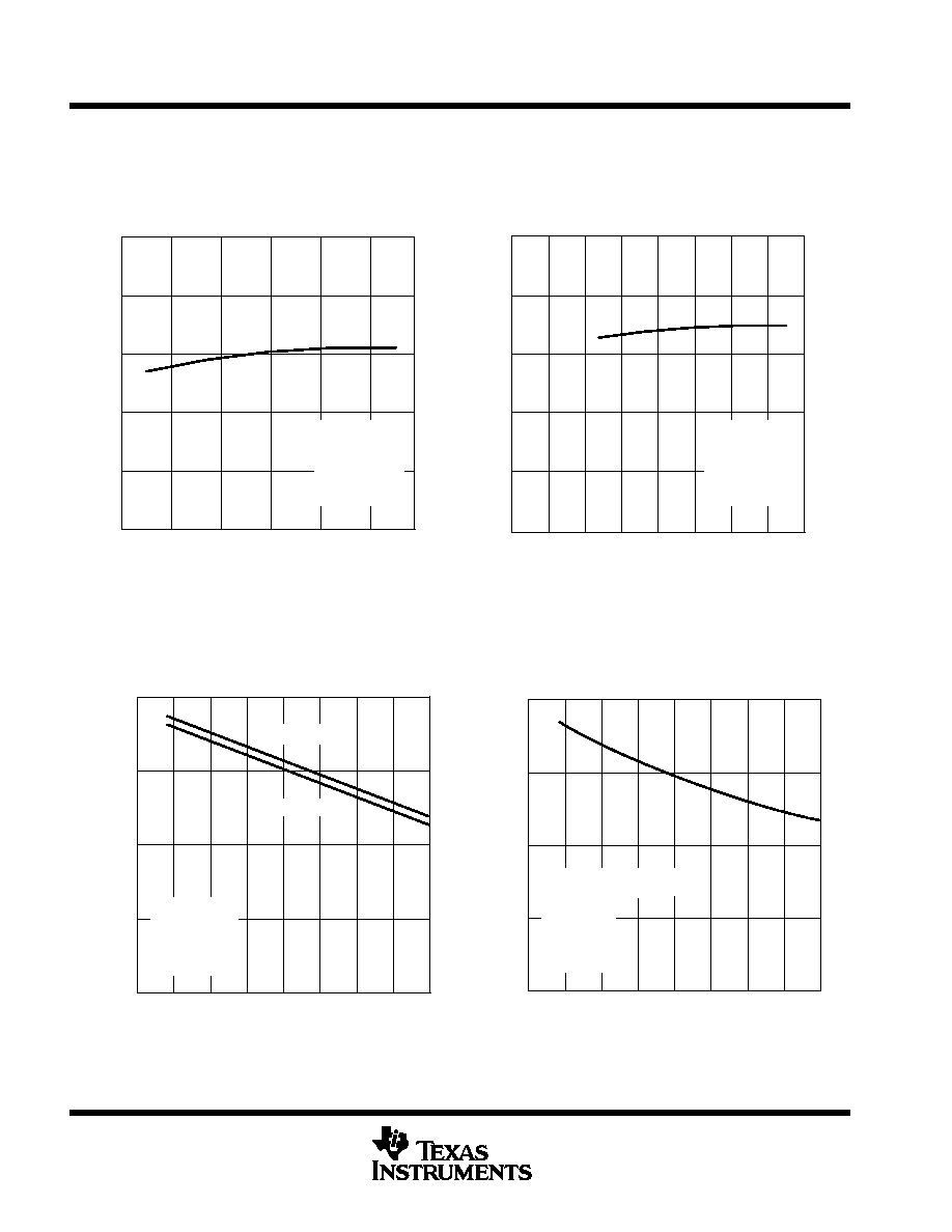
TL05x, TL05xA
ENHANCED-JFET LOW-OFFSET
OPERATIONAL AMPLIFIERS
SLOS178A ≠ FEBRUARY 1997 - REVISED FEBRUARY 2003
34
POST OFFICE BOX 655303
∑
DALLAS, TEXAS 75265
TYPICAL CHARACTERISTICS
Figure 65
¡¡¡¡
¡¡¡¡
¡¡¡¡
¡¡¡¡
¡¡¡¡
VI = 10 mV
RL = 2 k
CL = 25 pF
See Figure 4
TA = 25
∞
C
2.7
≠
Unity-Gain Bandwidth
≠
MHz
|VCC
±
| ≠ Supply Voltage ≠ V
16
3.2
4
6
8
10
12
14
2.8
2.9
3
3.1
B
1
TL052
UNITY-GAIN BANDWIDTH
vs
SUPPLY VOLTAGE
Figure 66
¡¡¡¡¡
¡¡¡¡¡
¡¡¡¡¡
¡¡¡¡¡
¡¡¡¡¡
2.4
≠
Unity-Gain Bandwidth
≠
MHz
|VCC
±
| ≠ Supply Voltage ≠ V
16
2.9
0
2
6
8
10
14
2.5
2.6
2.7
2.8
B
1
ŒŒŒŒ
ŒŒŒŒ
VI = 10 mV
ŒŒŒŒŒ
ŒŒŒŒŒ
RL = 2 k
ŒŒŒŒŒŒ
CL = 25 pF
ŒŒŒŒŒŒŒ
ŒŒŒŒŒŒŒ
See Figure 4
ŒŒŒŒŒ
ŒŒŒŒŒ
TA = 25
∞
C
4
12
TL054
UNITY-GAIN BANDWIDTH
vs
SUPPLY VOLTAGE
Figure 67
≠75
0
TA ≠ Free-Air Temperature ≠
∞
C
125
4
≠50
≠25
0
25
50
75
100
1
2
3
See Figure 4
VI = 10 mV
RL = 2 k
CL = 25 pF
VCC
±
=
±
15 V
VCC
±
=
±
5 V
≠
Unity-Gain Bandwidth
≠
MHz
B
1
TL051
UNITY-GAIN BANDWIDTH
vs
FREE-AIR TEMPERATURE
Figure 68
See Figure 4
VCC
±
=
±
5 V to
±
15 V
RL = 2 k
CL = 25 pF
TA = 25
∞
C
VI = 10 mV
≠75
0
TA ≠ Free-Air Temperature ≠
∞
C
125
4
≠50
≠25
0
25
50
75
100
1
2
3
≠
Unity-Gain Bandwidth
≠
MHz
B
1
TL052
UNITY-GAIN BANDWIDTH
vs
FREE-AIR TEMPERATURE
Data at high and low temperatures are applicable only within the rated operating free-air temperature ranges of the various devices.
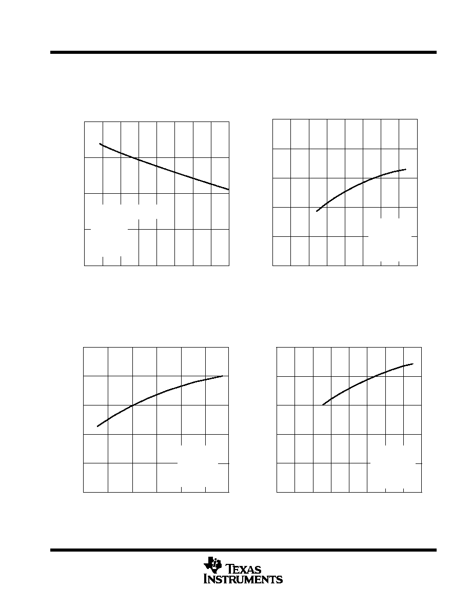
TL05x, TL05xA
ENHANCED-JFET LOW-OFFSET
OPERATIONAL AMPLIFIERS
SLOS178A ≠ FEBRUARY 1997 - REVISED FEBRUARY 2003
35
POST OFFICE BOX 655303
∑
DALLAS, TEXAS 75265
TYPICAL CHARACTERISTICS
Figure 69
See Figure 4
VCC
±
=
±
5 V to
±
15 V
RL = 2 k
CL = 25 pF
TA = 25
∞
C
VI = 10 mV
≠75
0
TA ≠ Free-Air Temperature ≠
∞
C
125
4
≠50
≠25
0
25
50
75
100
1
2
3
≠
Unity-Gain Bandwidth
≠
MHz
B
1
TL054
UNITY-GAIN BANDWIDTH
vs
FREE-AIR TEMPERATURE
Figure 70
0
55
∞
m
16
65
∞
2
4
6
8
10
12
14
57
∞
59
∞
61
∞
63
∞
|VCC
±
| ≠ Supply Voltage ≠ V
See Figure 4
TA = 25
∞
C
CL = 25 pF
RL = 2 k
VI = 10 mV
≠
Phase Margin
TL051
PHASE MARGIN
vs
SUPPLY VOLTAGE
Figure 71
55
∞
m
16
65
∞
4
6
8
10
12
14
57
∞
59
∞
61
∞
63
∞
|VCC
±
| ≠ Supply Voltage ≠ V
≠
Phase Margin
See Figure 4
TA = 25
∞
C
CL = 25 pF
RL = 2 k
VI = 10 mV
TL052
PHASE MARGIN
vs
SUPPLY VOLTAGE
Figure 72
55
∞
m
16
65
∞
0
4
8
10
12
14
57
∞
59
∞
61
∞
63
∞
|VCC
±
| ≠ Supply Voltage ≠ V
≠
Phase Margin
6
2
¡¡¡¡¡
¡¡¡¡¡
¡¡¡¡¡
¡¡¡¡¡
¡¡¡¡¡
See Figure 4
TA = 25
∞
C
CL = 25 pF
RL = 2 k
VI = 10 mV
TL054
PHASE MARGIN
vs
SUPPLY VOLTAGE
Data at high and low temperatures are applicable only within the rated operating free-air temperature ranges of the various devices.

TL05x, TL05xA
ENHANCED-JFET LOW-OFFSET
OPERATIONAL AMPLIFIERS
SLOS178A ≠ FEBRUARY 1997 - REVISED FEBRUARY 2003
36
POST OFFICE BOX 655303
∑
DALLAS, TEXAS 75265
TYPICAL CHARACTERISTICS
Figure 73
0
40
∞
CL ≠ Load Capacitance ≠ pF
100
70
∞
10
20
30
40
50
60
70
80
90
45
∞
50
∞
55
∞
60
∞
65
∞
VI = 10 mV
RL = 2 k
TA = 25
∞
C
See Figure 4
VCC
±
=
±
15 V
See Note A
VCC
±
=
±
5 V
m
≠
Phase Margin
TL051
PHASE MARGIN
vs
LOAD CAPACITANCE
Figure 74
0
CL ≠ Load Capacitance ≠ pF
70
∞
10
20
30
40
50
60
70
80
90
45
∞
50
∞
55
∞
60
∞
65
∞
VI = 10 mV
RL = 2 k
TA = 25
∞
C
See Figure 4
ŒŒŒŒŒ
VCC
±
=
±
15 V
See Note A
ŒŒŒŒŒ
ŒŒŒŒŒ
VCC
±
=
±
5 V
m
≠
Phase Margin
TL052
PHASE MARGIN
vs
LOAD CAPACITANCE
100
0
CL ≠ Load Capacitance ≠ pF
100
70
∞
10
20
30
40
50
60
70
80
90
45
∞
50
∞
55
∞
60
∞
65
∞
VI = 10 mV
RL = 2 k
TA = 25
∞
C
See Figure 4
ŒŒŒŒŒ
ŒŒŒŒŒ
VCC
±
=
±
15 V
See Note A
ŒŒŒŒŒ
VCC
±
=
±
5 V
m
≠
Phase Margin
TL054
PHASE MARGIN
vs
LOAD CAPACITANCE
Figure 75
Values of phase margin below a load capacitance of 25 pF were estimated.

TL05x, TL05xA
ENHANCED-JFET LOW-OFFSET
OPERATIONAL AMPLIFIERS
SLOS178A ≠ FEBRUARY 1997 - REVISED FEBRUARY 2003
37
POST OFFICE BOX 655303
∑
DALLAS, TEXAS 75265
TYPICAL CHARACTERISTICS
Figure 76
≠75
55
∞
TA ≠ Free-Air Temperature ≠
∞
C
125
65
∞
≠50
≠25
0
25
50
75
100
57
∞
59
∞
61
∞
63
∞
VCC
±
=
±
15 V
VCC
±
=
±
5 V
¡¡¡¡¡
¡¡¡¡¡
¡¡¡¡¡
¡¡¡¡¡
CL = 25 pF
VI = 10 mV
RL = 2 k
See Figure 4
m
≠
Phase Margin
TL051
PHASE MARGIN
vs
FREE-AIR TEMPERATURE
Figure 77
≠75
55
∞
TA ≠ Free-Air Temperature ≠
∞
C
125
65
∞
≠50
≠25
0
25
50
75
100
57
∞
59
∞
61
∞
63
∞
VCC
±
=
±
15 V
VCC
±
=
±
5 V
¡¡¡¡¡
¡¡¡¡¡
¡¡¡¡¡
¡¡¡¡¡
CL = 25 pF
VI = 10 mV
RL = 2 k
See Figure 4
m
≠
Phase Margin
TL052
PHASE MARGIN
vs
FREE-AIR TEMPERATURE
≠75
55
∞
TA ≠ Free-Air Temperature ≠
∞
C
125
65
∞
≠50
≠25
0
25
50
75
100
57
∞
59
∞
61
∞
63
∞
VCC
±
=
±
15 V
VCC
±
=
±
5 V
¡¡¡¡¡
¡¡¡¡¡
¡¡¡¡¡
¡¡¡¡¡
CL = 25 pF
VI = 10 mV
RL = 2 k
See Figure 4
m
≠
Phase Margin
TL054
PHASE MARGIN
vs
FREE-AIR TEMPERATURE
Figure 78
Data at high and low temperatures are applicable only within the rated operating free-air temperature ranges of the various devices.

TL05x, TL05xA
ENHANCED-JFET LOW-OFFSET
OPERATIONAL AMPLIFIERS
SLOS178A ≠ FEBRUARY 1997 - REVISED FEBRUARY 2003
38
POST OFFICE BOX 655303
∑
DALLAS, TEXAS 75265
TYPICAL CHARACTERISTICS
≠16
≠
Output V
oltage
≠
mV
t ≠ Time ≠
µ
s
1.2
16
0
0.2
0.4
0.6
0.8
1.0
≠12
≠8
≠4
0
4
8
12
VOLTAGE-FOLLOWER
SMALL-SIGNAL
PULSE RESPONSE
V
O
¡¡¡¡¡
¡¡¡¡¡
¡¡¡¡¡
¡¡¡¡¡
VCC
±
=
±
15 V
RL = 2 k
CL = 100 pF
TA = 25
∞
C
See Figure 1
Figure 79
≠8
t ≠ Time ≠
µ
s
6
8
0
1
2
3
4
5
≠6
≠4
≠2
0
2
4
6
VOLTAGE-FOLLOWER
LARGE-SIGNAL
PULSE RESPONSE
≠
Output V
oltage
≠
V
V
O
¡¡¡¡¡
¡¡¡¡¡
¡¡¡¡¡
¡¡¡¡¡
¡¡¡¡¡
VCC
±
=
±
15 V
RL = 2 k
CL = 100 pF
TA = 25
∞
C
See Figure 1
Figure 80
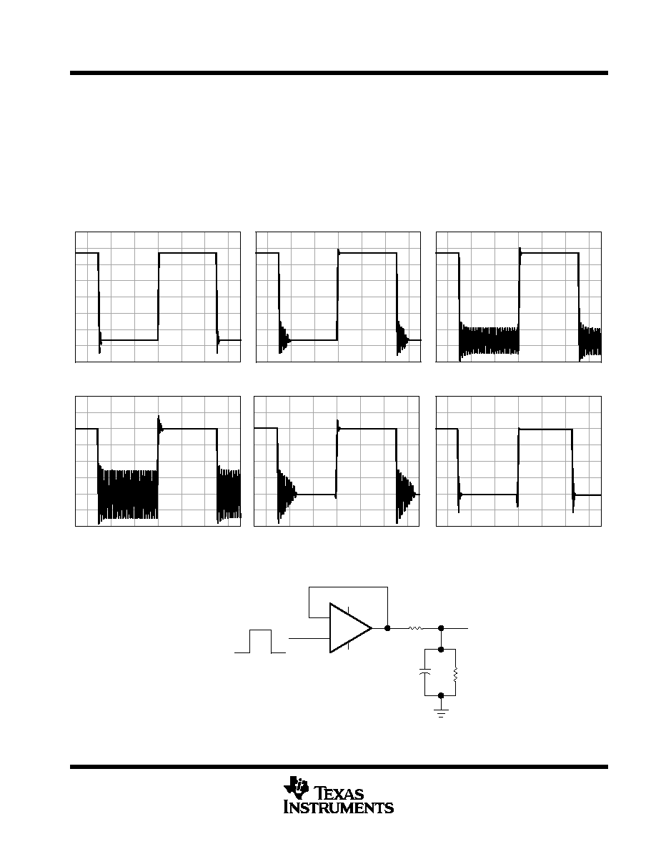
TL05x, TL05xA
ENHANCED-JFET LOW-OFFSET
OPERATIONAL AMPLIFIERS
SLOS178A ≠ FEBRUARY 1997 - REVISED FEBRUARY 2003
39
POST OFFICE BOX 655303
∑
DALLAS, TEXAS 75265
APPLICATION INFORMATION
output characteristics
All operating characteristics (except bandwidth and phase margin) are specified with 100-pF load capacitance.
The TL05x and TL05xA drive higher capacitive loads; however, as the load capacitance increases, the resulting
response pole occurs at lower frequencies, causing ringing, peaking, or even oscillation. The value of the load
capacitance at which oscillation occurs varies with production lots. If an application appears to be sensitive to
oscillation due to load capacitance, adding a small resistance in series with the load should alleviate the
problem. Capacitive loads of 1000 pF, and larger, may be driven if enough resistance is added in series with
the output (see Figure 81 and Figure 82).
(a) CL = 100 pF, R = 0
(b) CL = 300 pF, R = 0
(c) CL = 350 pF, R = 0
(d) CL = 1000 pF, R = 0
(e) CL = 1000 pF, R = 50
(f) CL = 1000 pF, R = 2 k
Figure 81. Effect of Capacitive Loads
+
≠
5 V
≠5 V
15 V
≠15 V
CL
(see Note A)
2 k
VO
R
NOTE A: CL includes fixture capacitance.
Figure 82. Test Circuit for Output Characteristics
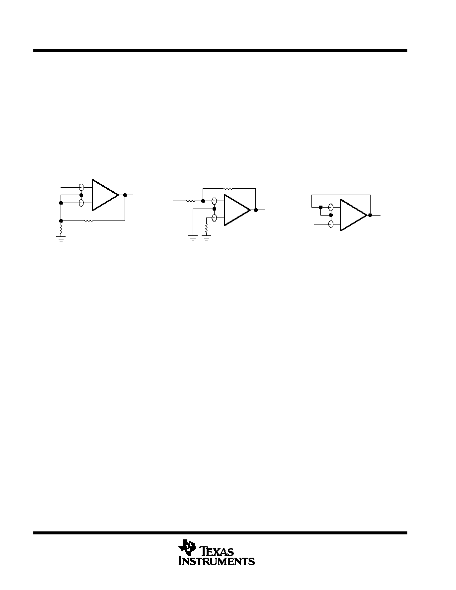
TL05x, TL05xA
ENHANCED-JFET LOW-OFFSET
OPERATIONAL AMPLIFIERS
SLOS178A ≠ FEBRUARY 1997 - REVISED FEBRUARY 2003
40
POST OFFICE BOX 655303
∑
DALLAS, TEXAS 75265
APPLICATION INFORMATION
input characteristics
The TL05x and TL05xA are specified with a minimum and a maximum input voltage that, if exceeded at either
input, could cause the device to malfunction.
Because of the extremely high input impedance and resulting low-bias current requirements, the TL05x and
TL05xA are well suited for low-level signal processing; however, leakage currents on printed-circuit boards and
sockets easily can exceed bias current requirements and cause degradation in system performance. It is good
practice to include guard rings around inputs (see Figure 83). These guards should be driven from a
low-impedance source at the same voltage level as the common-mode input.
Unused amplifiers should be connected as grounded unity-gain followers to avoid possible oscillation.
+
≠
+
≠
+
≠
VO
VO
VO
VI
VI
(a) NONINVERTING AMPLIFIER
(b) INVERTING AMPLIFIER
(c) UNITY-GAIN AMPLIFIER
VI
Figure 83. Use of Guard Rings
noise performance
The noise specifications in operational amplifier circuits are greatly dependent on the current in the first-stage
differential amplifier. The low input-bias current requirements of the TL05x and TL05xA result in a very low
current noise. This feature makes the devices especially favorable over bipolar devices when using values of
circuit impedance greater than 50 k
.

TL05x, TL05xA
ENHANCED-JFET LOW-OFFSET
OPERATIONAL AMPLIFIERS
SLOS178A ≠ FEBRUARY 1997 - REVISED FEBRUARY 2003
41
POST OFFICE BOX 655303
∑
DALLAS, TEXAS 75265
APPLICATION INFORMATION
phase meter
The phase meter in Figure 84 produces an output voltage of 10 mV per degree of phase delay between the two
input signals V
A
and V
B
. The reference signal V
A
must be the same frequency as V
B
. The TLC3702 comparators
(U1) convert these two input sine waves into
±
5-V square waves. Then, R1 and R4 provide level shifting prior
to the SN74HC109 dual J-K flip flops.
Flip-flop U2B is connected as a toggle flip-flop and generates a square wave at one-half the frequency of V
B
.
Flip-flop U2A also produces a square wave at one-half the input frequency. The pulse duration of U2A varies
from zero to one-half the period, where zero corresponds to zero phase delay between V
A
and V
B
and one-half
the period corresponds to V
B
lagging V
A
by 360 degrees.
The output pulse from U2A causes the TLC4066 (U3) switch to charge the TL05x (U4) integrator capacitors C1
and C2. As the phase delay approaches 360 degrees, the output of U4A approximates a square wave, and U2A
has an output of almost 2.5 V. U4B acts as a noninverting amplifier with a gain of 1.44 in order to scale the
0- to 2.5-V integrator output to a 0- to 3.6-V output range.
R8 and R10 provide output gain and zero-level calibration. This circuit operates over a 100-Hz to 10-kHz
frequency range.
+
≠
+
≠
+5 V
R2
100 k
R1
100 k
U1A
VA
S
1J
C1
U2A
1K
R
NC
U2B
2K
R3
VB
U1B
R6
10 k
R7
10 k
+5 V
S
2J
C1
R
NC
100 k
R4
100 k
U3
R5
C1
10 k
0.016
µ
F
C2
0.016
µ
F
U4A
U4B
VO
R9
20 k
R8
Gain
50 k
+5 V
R10
10 k
Zero
≠5 V
NOTE A: U1 = TLC3702; VCC
±
=
±
5 V
U2 = SN74HC109
U3 = TLC4066
U4, U5 = TL05x; VCC
±
=
±
5 V
Figure 84. Phase Meter

TL05x, TL05xA
ENHANCED-JFET LOW-OFFSET
OPERATIONAL AMPLIFIERS
SLOS178A ≠ FEBRUARY 1997 - REVISED FEBRUARY 2003
42
POST OFFICE BOX 655303
∑
DALLAS, TEXAS 75265
APPLICATION INFORMATION
precision constant-current source over temperature
A precision current source (see Figure 85) benefits from the high input impedance and stability of Texas
Instruments enhanced-JFET process. A low-current shunt regulator maintains 2.5 V between the inverting input
and the output of the TL05x. The negative feedback then forces 2.5 V across the current-setting resistor R;
therefore, the current to the load simply is 2.5 V divided by R.
Possible choices for the shunt regulator include the LT1004, LT1009, and LM385. If the regulator's cathode
connects to the operational amplifier output, this circuit sources load current. Similarly, if the cathode connects
to the inverting input, the circuit sinks current from the load. To minimize output current change with temperature,
R should be a metal film resistor with a low temperature coefficient. Also, this circuit must be operated with
split-voltage supplies.
+
≠
+
≠
150 pF
U2
+15 V
U1
≠15 V
R
100 k
IO
Load
V = 0 to 10 V
(a) SOURCE CURRENT LOAD
(b) SINK CURRENT LOAD
V = 0 to ≠10 V
Load
II
R
≠15 V
U1
+15 V
150 pF
U2
100 k
NOTE A: U1 = 1/2 TL05x
U2 = LM385, LT1004, or LT1009 voltage reference
I =
2.5 V
R
, R = Low-temperature-coefficient metal-film resistor
Figure 85. Precision Constant-Current Source
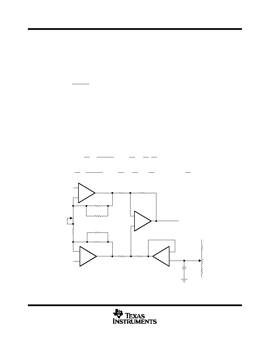
TL05x, TL05xA
ENHANCED-JFET LOW-OFFSET
OPERATIONAL AMPLIFIERS
SLOS178A ≠ FEBRUARY 1997 - REVISED FEBRUARY 2003
43
POST OFFICE BOX 655303
∑
DALLAS, TEXAS 75265
APPLICATION INFORMATION
instrumentation amplifier with adjustable gain/null
The instrumentation amplifier in Figure 86 benefits greatly from the high input impedance and stable input offset
voltage of the TL05xA. Amplifiers U1A, U1B, and U2A form the actual instrumentation amplifier, while U2B
provides offset null. Potentiometer R1 provides gain adjustment. With R1 = 2 k
, the circuit gain equals 100,
while with R1 = 200 k
, the circuit gain equals two. The following equation shows the instrumentation amplifier
gain as a function of R1:
A
V
+
1
)
R2
)
R3
R1
Readjusting the offset null is necessary when the circuit gain is changed. If U2B is needed for another
application, R7 can be terminated at ground. The low input offset voltage of the TL05xA minimizes the dc error
of the circuit. For best matching, all resistors should be one-percent tolerance. The matching between R4, R5,
R6, and R7 controls the CMRR of this application.
The following equation shows the output voltages when the input voltage equals zero. This dc error can be
nulled by adjusting the offset null potentiometer; however, any change in offset voltage over time or temperature
also creates an error. To calculate the error from changes in offset, consider the three offset components in the
equation as delta offsets, rather than initial offsets. The improved stability of Texas Instruments enhanced JFETs
minimizes the error resulting from change in input offset voltage with time. Assuming V
I
equals zero, V
O
can
be shown as a function of the offset voltage:
≠V
IO1
R3
R1
R7
R5
)
R7
1
)
R6
R4
)
R6
R4
1
)
R2
R1
)
V
IO3
1
)
R6
R4
V
O
+
V
IO2
1
)
R3
R1
R7
R5
)
R7
1
)
R6
R4
)
R2
R1
R6
R4
NOTE A: U1 and U2 = TL05xA; VCC
±
=
±
15 V.
100 k
U2A
+
≠
+
≠
+
≠
+
≠
VI≠
U1A
R4
10 k
R6
10 k
200 k
R2
10 M
100 k
10 turn
AV = 2 to 100
2 k
R1
U1B
VI+
R5
R7
U2B
0.1
µ
F
Offset Null
VCC≠
82 k
82 k
VCC+
R3
VO
10 k
10 k
10 M
1 k
Figure 86. Instrumentation Amplifier
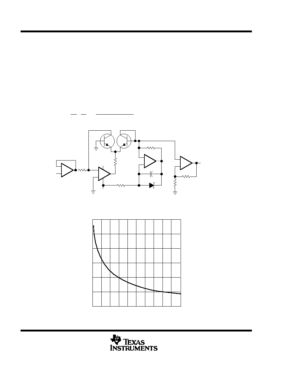
TL05x, TL05xA
ENHANCED-JFET LOW-OFFSET
OPERATIONAL AMPLIFIERS
SLOS178A ≠ FEBRUARY 1997 - REVISED FEBRUARY 2003
44
POST OFFICE BOX 655303
∑
DALLAS, TEXAS 75265
APPLICATION INFORMATION
high input impedance log amplifier
The low input offset voltage and high input impedance of the TL05xA creates a precision log amplifier (see
Figure 87). IC1 is a 2.5-V, low-current precision, shunt regulator. Transistors Q1 and Q2 must be a closely
matched npn pair. For best performance over temperature, R4 should be a metal-film resistor with a low
temperature coefficient.
In this circuit, U1A serves as a high-impedance unity-gain buffer. Amplifier U1B converts the input voltage to
a current through R1 and Q1. Amplifier U1C, IC1, and R4 form a 1-
µ
A temperature-stable current source that
sets the base-emitter voltage of Q2. U1D amplifies the difference between the base-emitter voltage of Q1 and
Q2 (see Figure 88). The output voltage is given by the following equation:
V
O
+
≠ 1
)
R6
R5
kT
q
In
V
I
R1
1
10
≠6
where k
+
1.38
10≠23, q
+
1.602
10≠19,
and T is Kelvin temperature
_
+
_
+
U1A
_
+
U1B
_
+
U1C
U1D
VI
R1
10 k
Q1
Q2
2N2484
R2
15 V
10 k
2.5 M
R4
150 pF
C1
IC1
270 k
R3
≠15V
R5
10 k
R6
10 k
VO
(see equation above)
NOTE A: U1A through U1D = TL05xA. IC1 = LM385, LT1004, or LT1009 voltage reference
Figure 87. Log Amplifier
0
1
2
3
4
5
6
≠
Differential V
oltage
Amplification
≠
dB
f ≠ Frequency ≠ Hz
7
8
9
10
≠0.4
≠0.35
≠0.3
≠0.25
≠0.2
≠0.15
≠0.1
¡¡
¡¡
¡¡
A
VD
Figure 88. Output Voltage vs Input Voltage for Log Amplifier
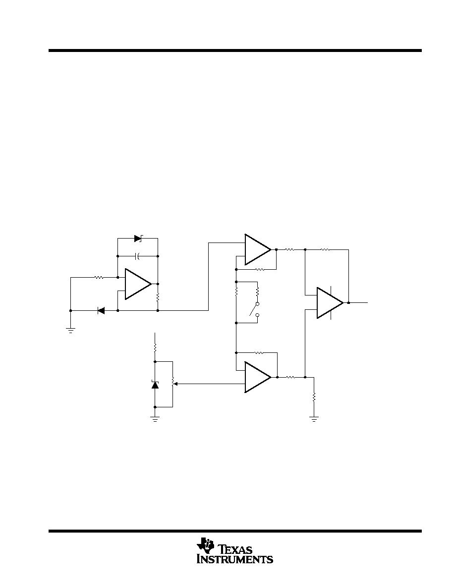
TL05x, TL05xA
ENHANCED-JFET LOW-OFFSET
OPERATIONAL AMPLIFIERS
SLOS178A ≠ FEBRUARY 1997 - REVISED FEBRUARY 2003
45
POST OFFICE BOX 655303
∑
DALLAS, TEXAS 75265
APPLICATION INFORMATION
analog thermometer
By combining a current source that does not vary over temperature with an instrumentation amplifier, a precise
analog thermometer can be built (see Figure 89). Amplifier U1A and IC1 establish a constant current through
the temperature-sensing diode D1. For this section of the circuit to operate correctly, the TL05x must use split
supplies, and R3 must be a metal-film resistor with a low temperature coefficient.
The temperature-sensitive voltage from the diode is compared to a temperature-stable voltage reference set
by IC2. R4 should be adjusted to provide the correct output voltage when the diode is at a known temperature.
Although this potentiometer resistance varies with temperature, the divider ratio of the potentiometer remains
constant.
Amplifiers U1B, U2A, and U2B form the instrumentation amplifier that converts the difference between the diode
and reference voltage to a voltage proportional to the temperature. With switch S1 closed, the amplifier gain
equals 5 and the output voltage is proportional to temperature in degrees Celsius. With S1 open, the amplifier
gain is 9 and the output is proportional to temperature in degrees Fahrenheit. Every time S1 is changed, R4 must
be recalibrated. By setting S1 correctly, the output voltage equals 10 mV per degree (C or F).
+
≠
+
≠
+
≠
IC1
C1
150 pF
R1
100 k
U1A
R3
10 k
(see Note B)
D1
(see Note A)
+15 V
R2
100 k
IC2
R4
50 k
U1B
R6
10 k
R5
5 k
R7
5 k
S1
(see Note C)
R8
10 k
U2A
R10
10 k
R11
R9
R12
10 k
10 k
+15 V
+
≠
≠15 V
10 k
VO
(see Note D)
U2B
NOTES: A. Temperature-sensing diode
(≠2 mV/
∞
C)
B. Metal-film resistor (low temperature coefficient)
C. Switch open for
∞
F and closed for
∞
C
D. VO
temperature; 10 mV/
∞
C or 10 mV/
∞
F
E. U1, U2 = TL05x. IC1, IC2 = LM385, LT1004, or LT1009 voltage reference
Figure 89. Analog Thermometer
TL05x, TL05xA
ENHANCED-JFET LOW-OFFSET
OPERATIONAL AMPLIFIERS
SLOS178A ≠ FEBRUARY 1997 - REVISED FEBRUARY 2003
46
POST OFFICE BOX 655303
∑
DALLAS, TEXAS 75265
APPLICATION INFORMATION
voltage-ratio-to-dB converter
The application in Figure 90 measures the amplitude ratio of two signals, then converts the ratio to decibels (see
Figure 91). The output voltage provides a resolution of 100 mV/dB. The two inputs can be either dc or sinusoidal
ac signals. When using ac signals, both signals should be the same frequency or output glitches will occur. For
measuring two input signals of different frequencies, extra filtering should be added after the rectifiers.
The circuit contains three low-offset TL05xA devices. Two of these devices provide the rectification and
logarithmic conversion of the inputs. The third TL05xA forms an instrumentation amplifier. The stage performing
the logarithmic conversion also requires two well-matched npn transistors.
The input signal first passes through a high-impedance unity-gain buffer U1A (U2A). Then U1B (U2B) rectifies
the input signal at a gain of 0.5, and U1C (U2C) provides a noninverting gain of 2, so that the system gain is
still one. U1D (U2D), R6 (R13), and Q1 (Q2) perform the logarithmic conversion of the rectified input signal. The
instrumentation amplifier formed by U3A, U3B, U3D scales the difference of the two logarithmic voltages by a
gain of 33.6. As a result, the output voltage equals 100 mV/dB. The 1-k
potentiometer on the input of U3C
calibrates the zero-dB reference level. The following equations are used to derive the relationship between the
input voltage ratio, expressed in decibels, and the output voltage.
X dB
+
20 log
V
A
V
B
+
20
In V
A
≠ V
B
In (10)
X dB
+
8.686 In V
A
≠ In V
B
V
BE(Q1)
+
kT
q In
V
A
R
I
S
V
BE(Q2)
+
kT
q In
V
B
R
I
S
D
V
BE
+
V
BE(Q1)
≠V
BE(Q2)
+
kT
q
In V
A
≠ In V
B
X dB
+
8.686
kT q
V
BE(Q1)
≠V
BE(Q2)
+
336
V
BE(Q1)
≠V
BE(Q2)
at 25
∞
C
where
k
+
1.38
10≠23, q
+
1.602
10≠19, and T is Kelvin temperature
This gives a resolution of 1 V/dB. Therefore, the gain of the instrumentation amplifier is set at 33.6 to obtain
100 mV/dB.
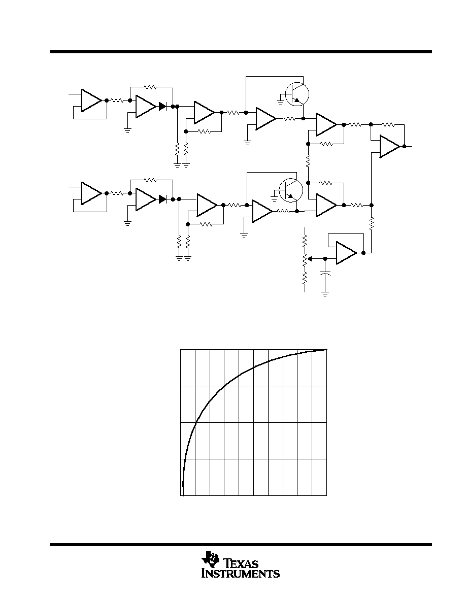
TL05x, TL05xA
ENHANCED-JFET LOW-OFFSET
OPERATIONAL AMPLIFIERS
SLOS178A ≠ FEBRUARY 1997 - REVISED FEBRUARY 2003
47
POST OFFICE BOX 655303
∑
DALLAS, TEXAS 75265
APPLICATION INFORMATION
_
+
_
+
_
+
_
+
_
+
_
+
_
+
_
+
_
+
_
+
_
+
_
+
U1A
U3A
U3B
U3C
U3D
U1B
U1C
U1D
U2A
U2B
U2C
U2D
VA
VB
VO
R1
20 k
R8
20 k
R2
10 k
R9
10 k
D1
D2
R3
30 k
R10
30 k
R4
10 k
R5
10 k
R6
10 k
R7
10 k
2N2484
Q1
Q2
R16
16.3 k
R18
10 k
R20
10 k
R11
10 k
R12
10 k
R13
10 k
2N2484
R14
10 k
R76
16.3 k
R19
10 k
R21
10 k
C1
15 V
≠15 V
82 k
1 k
82 k
NOTE A: U1A through U3D = TL05xA, VCC
±
=
±
15 V. D1 and D2 = 1N914.
Figure 90. Voltage Ratio-to-dB Converter
0
1
2
3
4
5
6
≠
Output V
oltage
≠
V
7
8
9
10
≠2
≠1
0
1
2
Ratio ≠ VA/VB
V
O
Figure 91. Output Voltage vs the Ratio of the Input Voltages for Voltage-to-dB Converter
TL05x, TL05xA
ENHANCED-JFET LOW-OFFSET
OPERATIONAL AMPLIFIERS
SLOS178A ≠ FEBRUARY 1997 - REVISED FEBRUARY 2003
48
POST OFFICE BOX 655303
∑
DALLAS, TEXAS 75265
APPLICATION INFORMATION
macromodel information
Macromodel information provided was derived using Microsim Parts
, the model-generation software used
with Microsim PSpice
. The Boyle macromodel (see Note 6 and subcircuit Figure 92) are generated using the
TL05x typical electrical and operating characteristics at T
A
= 25
∞
C. Using this information, output simulations
of the following key parameters can be generated to a tolerance of 20% (in most cases):
D
Maximum positive output voltage swing
D
Maximum negative output voltage swing
D
Slew rate
D
Quiescent power dissipation
D
Input bias current
D
Open-loop voltage amplification
D
Unity-gain frequency
D
Common-mode rejection ratio
D
Phase margin
D
DC output resistance
D
AC output resistance
D
Short-circuit output current limit
NOTE 6: G. R. Boyle, B. M. Cohn, D. O. Pederson, and J. E. Solomon, "Macromodeling of Integrated Circuit Operational Amplifiers", IEEE Journal
of Solid-State Circuits, SC-9, 353 (1974).
OUT
+
≠
+
≠
+
≠
+
≠
+
≠
+
≠
+
≠
+
≠
+
≠
.SUBCKT TL05x 1 2 3 4 5
C1
11
12
3.988E≠12
C2
6
7
15.00E≠12
DC
5
53
DX
DE
54
5
DX
DLP
90
91
DX
DLN
92
90
DX
DP
4
3
DX
EGND 99
0
POLY (2) (3,0) (4,0) 0 .5 .5
FB
7
99
POLY (5) VB VC VE VLP
+ VLN 0 2.875E6 ≠3E6 3E6 3E6 ≠3E6
GA
6
0
11
12 292.2E≠6
GCM 0
6
10
99 6.542E≠9
ISS
3
10
DC 300.0E≠6
HLIM 90
0
VLIM 1K
J1
11
2
10 JX
J2
12
1
10 JX
R2
6
9
100.0E3
RD1
4
11
3.422E3
RD2
4
12
3.422E3
R01
8
5
125
R02
7
99
125
RP
3
4
11.11E3
RSS
10
99
666.7E6
VB
9
0
DC 0
VC 3 53
DC
3
VE
54
4
DC 3.7
VLIM 7
8
DC 0
VLP
91
0
DC 28
VLN
0
92
DC 28
.MODEL DX D (IS=800.0E≠18)
.MODEL JX PJF (IS=15.00E≠12 BETA=185.2E≠6
+ VTO=≠.1)
.ENDS
VCC+
RP
IN≠
2
IN+
3
VCC≠
VAD
RD1
11
J1
J2
10
RSS
ISS
3
12
RD2
60
VE
54
DE
DP
VC
DC
4
C1
53
R2
6
9
EGND
VB
FB
C2
GCM
GA
VLIM
8
5
RO1
RO2
HLIM
90
DLP
91
DLN
92
VLN
VLP
99
7
Figure 92. Boyle Macromodel and Subcircuit
PSpice and Parts are trademarks of MicroSim Corporation.
Macromodels, simulation models, or other models provided by TI,
directly or indirectly, are not warranted by TI as fully representing all
of the specification and operating characteristics of the
semiconductor product to which the model relates.
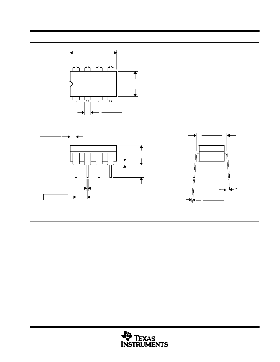
MECHANICAL DATA
MCER001A ≠ JANUARY 1995 ≠ REVISED JANUARY 1997
1
POST OFFICE BOX 655303
∑
DALLAS, TEXAS 75265
JG (R-GDIP-T8)
CERAMIC DUAL-IN-LINE
0.310 (7,87)
0.290 (7,37)
0.014 (0,36)
0.008 (0,20)
Seating Plane
4040107/C 08/96
5
4
0.065 (1,65)
0.045 (1,14)
8
1
0.020 (0,51) MIN
0.400 (10,16)
0.355 (9,00)
0.015 (0,38)
0.023 (0,58)
0.063 (1,60)
0.015 (0,38)
0.200 (5,08) MAX
0.130 (3,30) MIN
0.245 (6,22)
0.280 (7,11)
0.100 (2,54)
0
∞
≠15
∞
NOTES: A. All linear dimensions are in inches (millimeters).
B. This drawing is subject to change without notice.
C. This package can be hermetically sealed with a ceramic lid using glass frit.
D. Index point is provided on cap for terminal identification.
E. Falls within MIL STD 1835 GDIP1-T8

MECHANICAL DATA
MCER002C ≠ JANUARY 1995 ≠ REVISED JUNE 1999
1
POST OFFICE BOX 655303
∑
DALLAS, TEXAS 75265
J (R-GDIP-T**)
CERAMIC DUAL-IN-LINE
1
20
0.290
(7,87)
0.310
0.975
(24,77)
(23,62)
0.930
(7,37)
0.245
(6,22)
(7,62)
0.300
16
14
PINS **
0.290
(7,87)
0.310
0.785
(19,94)
(19,18)
0.755
(7,37)
0.310
(7,87)
(7,37)
0.290
0.755
(19,18)
(19,94)
0.785
0.245
(6,22)
(7,62)
0.300
A
0.300
(7,62)
(6,22)
0.245
A MIN
A MAX
B MAX
B MIN
C MIN
C MAX
DIM
0
∞
≠15
∞
Seating Plane
0.014 (0,36)
0.008 (0,20)
4040083/E 03/99
C
8
7
0.020 (0,51) MIN
B
0.070 (1,78)
0.100 (2,54)
0.065 (1,65)
0.045 (1,14)
14 LEADS SHOWN
14
0.015 (0,38)
0.023 (0,58)
0.100 (2,54)
0.200 (5,08) MAX
0.130 (3,30) MIN
NOTES: A. All linear dimensions are in inches (millimeters).
B. This drawing is subject to change without notice.
C. This package is hermetically sealed with a ceramic lid using glass frit.
D. Index point is provided on cap for terminal identification.
E. Falls within MIL STD 1835 GDIP1-T14, GDIP1-T16, and GDIP1-T20
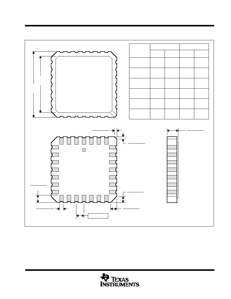
MECHANICAL DATA
MLCC006B ≠ OCTOBER 1996
1
POST OFFICE BOX 655303
∑
DALLAS, TEXAS 75265
FK (S-CQCC-N**)
LEADLESS CERAMIC CHIP CARRIER
4040140 / D 10/96
28 TERMINAL SHOWN
B
0.358
(9,09)
MAX
(11,63)
0.560
(14,22)
0.560
0.458
0.858
(21,8)
1.063
(27,0)
(14,22)
A
NO. OF
MIN
MAX
0.358
0.660
0.761
0.458
0.342
(8,69)
MIN
(11,23)
(16,26)
0.640
0.739
0.442
(9,09)
(11,63)
(16,76)
0.962
1.165
(23,83)
0.938
(28,99)
1.141
(24,43)
(29,59)
(19,32)
(18,78)
**
20
28
52
44
68
84
0.020 (0,51)
TERMINALS
0.080 (2,03)
0.064 (1,63)
(7,80)
0.307
(10,31)
0.406
(12,58)
0.495
(12,58)
0.495
(21,6)
0.850
(26,6)
1.047
0.045 (1,14)
0.045 (1,14)
0.035 (0,89)
0.035 (0,89)
0.010 (0,25)
12
13
14
15
16
18
17
11
10
8
9
7
5
4
3
2
0.020 (0,51)
0.010 (0,25)
6
1
28
26
27
19
21
B SQ
A SQ
22
23
24
25
20
0.055 (1,40)
0.045 (1,14)
0.028 (0,71)
0.022 (0,54)
0.050 (1,27)
NOTES: A. All linear dimensions are in inches (millimeters).
B. This drawing is subject to change without notice.
C. This package can be hermetically sealed with a metal lid.
D. The terminals are gold plated.
E. Falls within JEDEC MS-004
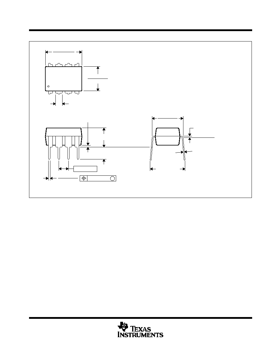
MECHANICAL DATA
MPDI001A ≠ JANUARY 1995 ≠ REVISED JUNE 1999
1
POST OFFICE BOX 655303
∑
DALLAS, TEXAS 75265
P (R-PDIP-T8)
PLASTIC DUAL-IN-LINE
8
4
0.015 (0,38)
Gage Plane
0.325 (8,26)
0.300 (7,62)
0.010 (0,25) NOM
MAX
0.430 (10,92)
4040082/D 05/98
0.200 (5,08) MAX
0.125 (3,18) MIN
5
0.355 (9,02)
0.020 (0,51) MIN
0.070 (1,78) MAX
0.240 (6,10)
0.260 (6,60)
0.400 (10,60)
1
0.015 (0,38)
0.021 (0,53)
Seating Plane
M
0.010 (0,25)
0.100 (2,54)
NOTES: A. All linear dimensions are in inches (millimeters).
B. This drawing is subject to change without notice.
C. Falls within JEDEC MS-001
For the latest package information, go to http://www.ti.com/sc/docs/package/pkg_info.htm
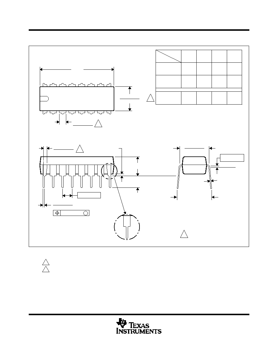
MECHANICAL
MPDI002C ≠ JANUARY 1995 ≠ REVISED DECEMBER 20002
1
POST OFFICE BOX 655303
∑
DALLAS, TEXAS 75265
N (R-PDIP-T**)
PLASTIC DUAL-IN-LINE PACKAGE
BB
AC
AD
0.325 (8,26)
0.300 (7,62)
0.010 (0,25) NOM
Gauge Plane
0.015 (0,38)
0.430 (10,92) MAX
20
1.060
(26,92)
0.940
(23,88)
18
0.920
0.850
14
0.775
0.745
(19,69)
(18,92)
16
0.775
(19,69)
(18,92)
0.745
A MIN
DIM
A MAX
PINS **
(23,37)
(21,59)
Seating Plane
14/18 PIN ONLY
20 pin vendor option
4040049/E 12/2002
9
8
0.070 (1,78)
A
0.045 (1,14)
0.020 (0,51) MIN
16
1
0.015 (0,38)
0.021 (0,53)
0.200 (5,08) MAX
0.125 (3,18) MIN
0.240 (6,10)
0.260 (6,60)
M
0.010 (0,25)
0.100 (2,54)
16 PINS SHOWN
MS-100
VARIATION
AA
C
D
D
D
0.030 (0,76)
0.045 (1,14)
NOTES: A. All linear dimensions are in inches (millimeters).
B. This drawing is subject to change without notice.
C. Falls within JEDEC MS-001, except 18 and 20 pin minimum body lrngth (Dim A).
D. The 20 pin end lead shoulder width is a vendor option, either half or full width.

MECHANICAL DATA
MSOI002B ≠ JANUARY 1995 ≠ REVISED SEPTEMBER 2001
1
POST OFFICE BOX 655303
∑
DALLAS, TEXAS 75265
D (R-PDSO-G**)
PLASTIC SMALL-OUTLINE PACKAGE
8 PINS SHOWN
8
0.197
(5,00)
A MAX
A MIN
(4,80)
0.189
0.337
(8,55)
(8,75)
0.344
14
0.386
(9,80)
(10,00)
0.394
16
DIM
PINS **
4040047/E 09/01
0.069 (1,75) MAX
Seating Plane
0.004 (0,10)
0.010 (0,25)
0.010 (0,25)
0.016 (0,40)
0.044 (1,12)
0.244 (6,20)
0.228 (5,80)
0.020 (0,51)
0.014 (0,35)
1
4
8
5
0.150 (3,81)
0.157 (4,00)
0.008 (0,20) NOM
0
∞
≠ 8
∞
Gage Plane
A
0.004 (0,10)
0.010 (0,25)
0.050 (1,27)
NOTES: A. All linear dimensions are in inches (millimeters).
B. This drawing is subject to change without notice.
C. Body dimensions do not include mold flash or protrusion, not to exceed 0.006 (0,15).
D. Falls within JEDEC MS-012

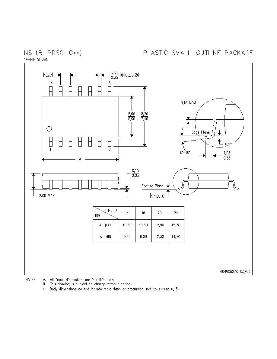

IMPORTANT NOTICE
Texas Instruments Incorporated and its subsidiaries (TI) reserve the right to make corrections, modifications,
enhancements, improvements, and other changes to its products and services at any time and to discontinue
any product or service without notice. Customers should obtain the latest relevant information before placing
orders and should verify that such information is current and complete. All products are sold subject to TI's terms
and conditions of sale supplied at the time of order acknowledgment.
TI warrants performance of its hardware products to the specifications applicable at the time of sale in
accordance with TI's standard warranty. Testing and other quality control techniques are used to the extent TI
deems necessary to support this warranty. Except where mandated by government requirements, testing of all
parameters of each product is not necessarily performed.
TI assumes no liability for applications assistance or customer product design. Customers are responsible for
their products and applications using TI components. To minimize the risks associated with customer products
and applications, customers should provide adequate design and operating safeguards.
TI does not warrant or represent that any license, either express or implied, is granted under any TI patent right,
copyright, mask work right, or other TI intellectual property right relating to any combination, machine, or process
in which TI products or services are used. Information published by TI regarding third≠party products or services
does not constitute a license from TI to use such products or services or a warranty or endorsement thereof.
Use of such information may require a license from a third party under the patents or other intellectual property
of the third party, or a license from TI under the patents or other intellectual property of TI.
Reproduction of information in TI data books or data sheets is permissible only if reproduction is without
alteration and is accompanied by all associated warranties, conditions, limitations, and notices. Reproduction
of this information with alteration is an unfair and deceptive business practice. TI is not responsible or liable for
such altered documentation.
Resale of TI products or services with statements different from or beyond the parameters stated by TI for that
product or service voids all express and any implied warranties for the associated TI product or service and
is an unfair and deceptive business practice. TI is not responsible or liable for any such statements.
Mailing Address:
Texas Instruments
Post Office Box 655303
Dallas, Texas 75265
Copyright
2003, Texas Instruments Incorporated