 | –≠–ª–µ–∫—Ç—Ä–æ–Ω–Ω—ã–π –∫–æ–º–ø–æ–Ω–µ–Ω—Ç: TL052CP | –°–∫–∞—á–∞—Ç—å:  PDF PDF  ZIP ZIP |

TL05x, TL05xA, TL05xY
ENHANCED-JFET LOW-OFFSET
OPERATIONAL AMPLIFIERS
SLOS178 ≠ FEBRUARY 1997
1
POST OFFICE BOX 655303
∑
DALLAS, TEXAS 75265
D
Direct Upgrades to TL07x and TL08x BiFET
Operational Amplifiers
D
Faster Slew Rate (20 V/
µ
s Typ) Without
Increased Power Consumption
D
On-Chip Offset Voltage Trimming for
Improved DC Performance and Precision
Grades Are Available (1.5 mV, TL051A)
D
Available in TSSOP for Small Form-Factor
Designs
description
The TL05x series of JFET-input operational amplifiers offers improved dc and ac characteristics over the TL07x
and TL08x families of BiFET operational amplifiers. On-chip zener trimming of offset voltage yields precision
grades as low as 1.5 mV (TL051A) for greater accuracy in dc-coupled applications. Texas Instruments improved
BiFET process and optimized designs also yield improved bandwidth and slew rate without increased power
consumption. The TL05x devices are pin-compatible with the TL07x and TL08x and can be used to upgrade
existing circuits or for optimal performance in new designs.
BiFET operational amplifiers offer the inherently higher input impedance of the JFET-input transistors, without
sacrificing the output drive associated with bipolar amplifiers. This makes them better suited for interfacing with
high-impedance sensors or very low-level ac signals. They also feature inherently better ac response than
bipolar or CMOS devices having comparable power consumption.
The TL05x family was designed to offer higher precision and better ac response than the TL08x with the low
noise floor of the TL07x. Designers requiring significantly faster ac response or ensured lower noise should
consider the Excalibur TLE208x and TLE207x families of BiFET operational amplifiers.
AVAILABLE OPTIONS
PACKAGED DEVICES
CHIP
TA
VIOmax
AT 25
∞
C
SMALL
OUTLINE
(D)
CHIP
CARRIER
(FK)
CERAMIC
DIP
(J)
CERAMIC
DIP
(JG)
PLASTIC
DIP
(N)
PLASTIC
DIP
(P)
CHIP
FORM
(Y)
800
µ
V
TL051ACD
TL052ACD
--
--
--
--
TL051ACP
TL052ACP
TL051Y
0
∞
C to 70
∞
C
1.5 mV
TL051CD
TL052CD
TL054ACD
--
--
--
TL054ACN
TL051CP
TL052CP
TL051Y
TL052Y
TL054Y
4 mV
TL054CD
--
--
--
TL054CN
--
800
µ
V
TL051AID
TL052AID
--
--
--
--
TL051AIP
TL052AIP
≠ 40
∞
C to 85
∞
C
1.5 mV
TL051ID
TL052ID
TL054AID
--
--
--
TL054AIN
TL051IP
TL052IP
--
4 mV
TL054ID
--
--
TL054IN
--
800
µ
V
TL051AMD
TL052AMD
TL051AMFK
TL052AMFK
--
TL051AMJG
TL052AMJG
--
TL051AMP
TL052AMP
≠ 55
∞
C to 125
∞
C
1.5 mV
TL051MD
TL052MD
TL054AMD
TL051MFK
TL052MFK
TL054AMFK
TL054AMJ
TL051MJG
TL052MJG
TL054AMN
TL051MP
TL052MP
--
4 mV
TL054MD
TL054MFK
TL054MJ
--
TL054MN
--
The D packages are available taped and reeled. Add R suffix to device type (e.g., TL054CDR).
Chip forms are tested at 25
∞
C.
Please be aware that an important notice concerning availability, standard warranty, and use in critical applications of
Texas Instruments semiconductor products and disclaimers thereto appears at the end of this data sheet.
Copyright
©
1997, Texas Instruments Incorporated
PRODUCTION DATA information is current as of publication date.
Products conform to specifications per the terms of Texas Instruments
standard warranty. Production processing does not necessarily include
testing of all parameters.

TL05x, TL05xA, TL05xY
ENHANCED-JFET LOW-OFFSET
OPERATIONAL AMPLIFIERS
SLOS178 ≠ FEBRUARY 1997
2
POST OFFICE BOX 655303
∑
DALLAS, TEXAS 75265
description (continued)
Because BiFET operational amplifiers are designed for use with dual power supplies, care must be taken to
observe common-mode input voltage limits and output swing when operating from a single supply. DC biasing
of the input signal is required and loads should be terminated to a virtual-ground node at midsupply. Texas
Instruments TLE2426 integrated virtual ground generator is useful when operating BiFET amplifiers from single
supplies.
The TL05x are fully specified at
±
15 V and
±
5 V. For operation in low-voltage and/or single-supply systems,
Texas Instruments LinCMOS families of operational amplifiers (TLC-prefix) are recommended. When moving
from BiFET to CMOS amplifiers, particular attention should be paid to the slew rate and bandwidth
requirements, and also the output loading.
3
2
1 20 19
9 10 11 12 13
4
5
6
7
8
18
17
16
15
14
4IN +
NC
V
CC ≠
NC
3IN +
1IN +
NC
V
CC +
NC
2IN +
1IN ≠
1OUT
NC
3OUT
3IN ≠
4IN ≠
2IN ≠
NC
4OUT
2OUT
1
2
3
4
5
6
7
14
13
12
11
10
9
8
1OUT
1IN ≠
1IN +
V
CC +
2IN +
2IN ≠
2OUT
4OUT
4IN ≠
4IN +
V
CC ≠
3IN +
3IN ≠
3OUT
1
2
3
4
8
7
6
5
OFFSET N1
IN ≠
IN +
V
CC ≠
NC
V
CC +
OUT
OFFSET N2
3
2
1 20 19
9 10 11 12 13
4
5
6
7
8
18
17
16
15
14
NC
V
CC +
NC
OUT
NC
NC
IN ≠
NC
IN +
NC
TL051
FK PACKAGE
(TOP VIEW)
NC
OFFSET
N1
NC
OFFSET
N2
NC
NC
NC
NC
NC ≠ No internal connection
CC
≠
V
NC
1
2
3
4
8
7
6
5
1OUT
1IN ≠
1IN +
V
CC ≠
V
CC +
2OUT
2IN ≠
2IN +
3
2
1 20 19
9 10 11 12 13
4
5
6
7
8
18
17
16
15
14
NC
2OUT
NC
2IN ≠
NC
NC
1IN ≠
NC
1IN+
NC
TL052
FK PACKAGE
(TOP VIEW)
NC
1OUT
NC
2IN +
NC
NC
NC
NC
CC
+
V
CC
≠
V
TL054
D, J, OR N PACKAGE
(TOP VIEW)
TL054
FK PACKAGE
(TOP VIEW)
TL051
D, JG, OR P PACKAGE
(TOP VIEW)
TL052
D, JG, OR P PACKAGE
(TOP VIEW)
TL05x, TL05xA, TL05xY
ENHANCED-JFET LOW-OFFSET
OPERATIONAL AMPLIFIERS
SLOS178 ≠ FEBRUARY 1997
3
POST OFFICE BOX 655303
∑
DALLAS, TEXAS 75265
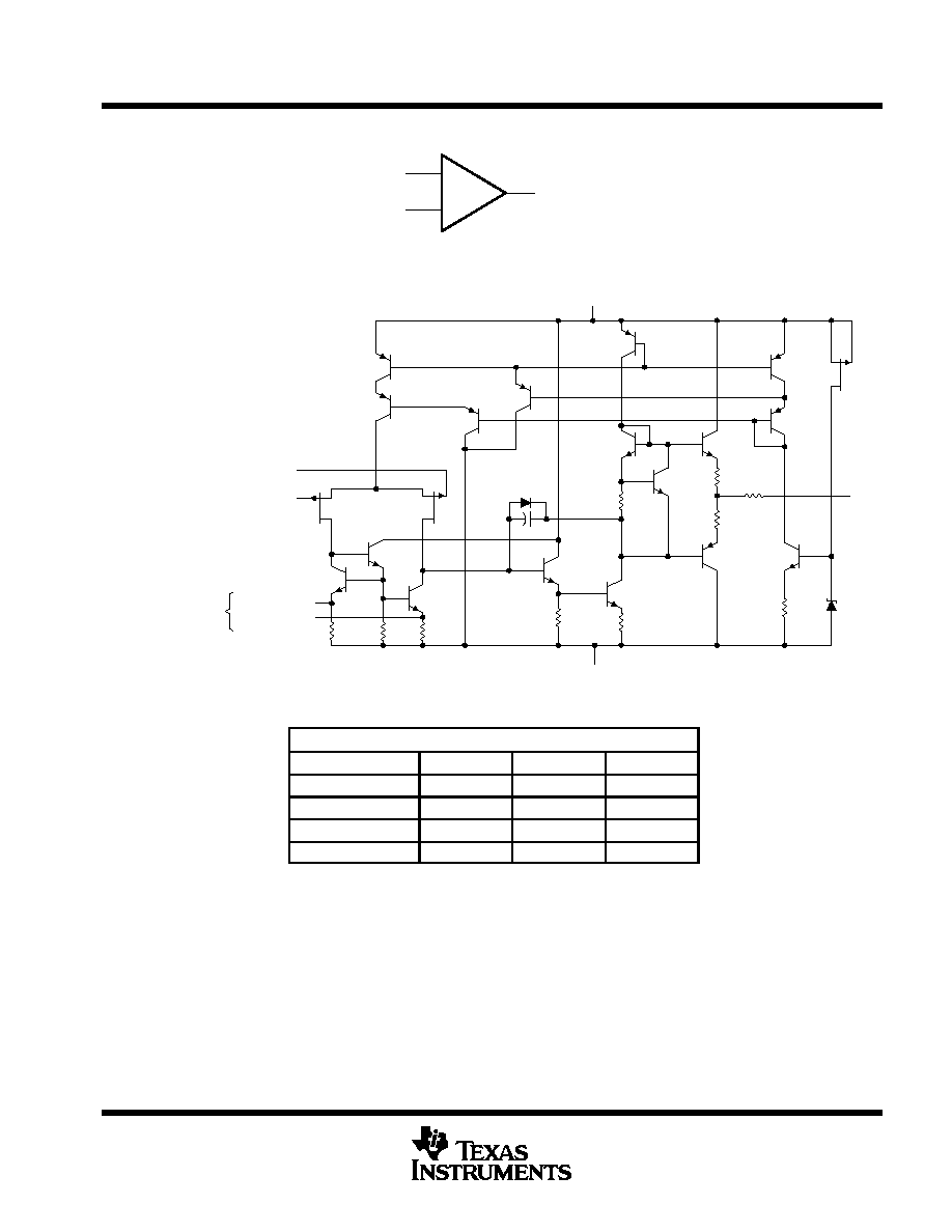
symbol (each amplifier)
+
≠
IN ≠
IN +
OUT
equivalent schematic (each amplifier)
R9
OFFSET N2
OFFSET N1
IN ≠
IN +
Q2
Q3
Q7
VCC +
Q14
Q6
R4
Q8
Q10
R7
Q11
R6
C1
Q9
Q5
Q4
R5
R1
Q1
JF1
JF2
Q13
Q16
R8
JF3
Q15
Q17
OUT
VCC ≠
R2
R3
Q12
R10
D2
D1
See Note A
NOTE A: OFFSET N1 and OFFSET N2 are only available on the TL051x.
ACTUAL DEVICE COMPONENT COUNT
COMPONENT
TL051
TL052
TL054
Transistors
20
34
62
Resistors
10
19
37
Diodes
2
3
5
Capacitors
1
2
4
These figures include all four amplifiers and all ESD, bias, and trim circuitry.
TL05x, TL05xA, TL05xY
ENHANCED-JFET LOW-OFFSET
OPERATIONAL AMPLIFIERS
SLOS178 ≠ FEBRUARY 1997
4
POST OFFICE BOX 655303
∑
DALLAS, TEXAS 75265
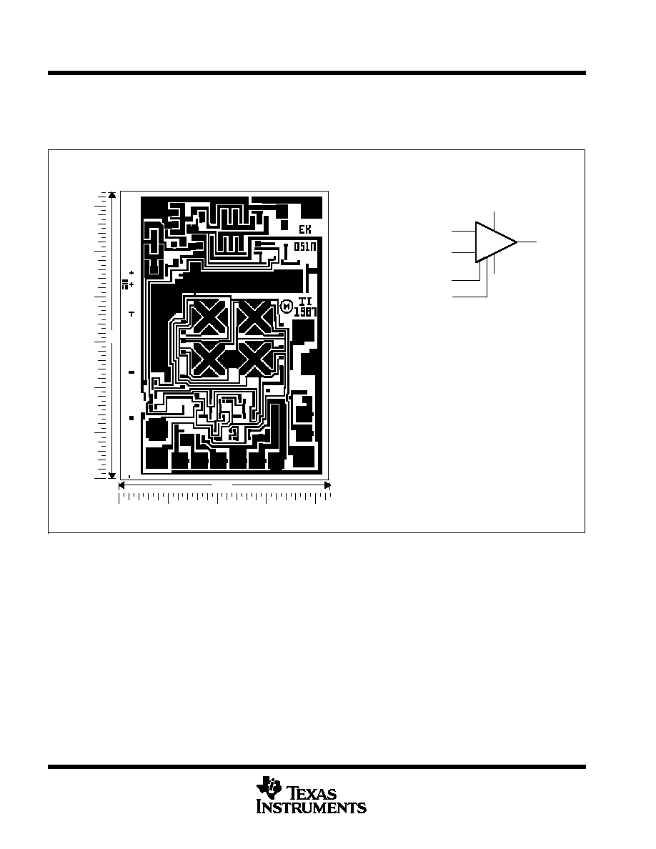
TL051Y chip information
This chip, when properly assembled, displays characteristics similar to the TL051. Thermal compression or
ultrasonic bonding may be used on the doped-aluminum bonding pads. Chips may be mounted with conductive
epoxy or a gold-silicon preform.
BONDING PAD ASSIGNMENTS
CHIP THICKNESS: 15 MILS TYPICAL
BONDING PADS: 4
◊
4 MILS MINIMUM
TJmax = 150
∞
C
TOLERANCES ARE
±
10%.
ALL DIMENSIONS ARE IN MILS.
PIN (4) IS INTERNALLY CONNECTED
TO BACKSIDE OF CHIP.
+
≠
OUT
IN +
IN ≠
VCC+
(7)
(3)
(2)
(6)
(1)
(4)
(5)
VCC ≠
OFFSET N1
OFFSET N2
63
43
(1)
(2)
(3)
(4)
(5)
(6)
(7)

TL05x, TL05xA, TL05xY
ENHANCED-JFET LOW-OFFSET
OPERATIONAL AMPLIFIERS
SLOS178 ≠ FEBRUARY 1997
5
POST OFFICE BOX 655303
∑
DALLAS, TEXAS 75265
TL052Y chip information
This chip, when properly assembled, displays characteristics similar to the TL052. Thermal compression or
ultrasonic bonding may be used on the doped-aluminum bonding pads. Chips may be mounted with conductive
epoxy or a gold-silicon preform.
BONDING PAD ASSIGNMENTS
CHIP THICKNESS: 15 MILS TYPICAL
BONDING PADS: 4
◊
4 MILS MINIMUM
TJmax = 150
∞
C
TOLERANCES ARE
±
10%.
ALL DIMENSIONS ARE IN MILS.
PIN (4) IS INTERNALLY CONNECTED
TO BACKSIDE OF CHIP.
+
≠
1OUT
1IN +
1IN ≠
VCC+
(8)
(6)
(3)
(2)
(5)
(1)
≠
+
(7)
2IN +
2IN ≠
2OUT
(4)
VCC ≠
(1)
(2)
(3)
(4)
(5)
(6)
(7)
(8)
66
72