 | –≠–ª–µ–∫—Ç—Ä–æ–Ω–Ω—ã–π –∫–æ–º–ø–æ–Ω–µ–Ω—Ç: TL062B | –°–∫–∞—á–∞—Ç—å:  PDF PDF  ZIP ZIP |
TL061, TL061A, TL061B, TL061Y, TL062, TL062A
TL062B, TL062Y, TL064, TL064A, TL064B, TL064Y
LOW-POWER JFET-INPUT OPERATIONAL AMPLIFIERS
SLOS078F ≠ NOVEMBER 1978 ≠ REVISED JANUARY 1999
1
POST OFFICE BOX 655303
∑
DALLAS, TEXAS 75265
D
Very Low Power Consumption
D
Typical Supply Current . . . 200
µ
A
(Per Amplifier)
D
Wide Common-Mode and Differential
Voltage Ranges
D
Low Input Bias and Offset Currents
D
Common-Mode Input Voltage Range
Includes V
CC+
D
Output Short-Circuit Protection
D
High Input Impedance . . . JFET-Input Stage
D
Internal Frequency Compensation
D
Latch-Up-Free Operation
D
High Slew Rate . . . 3.5 V/
µ
s Typ
description
The JFET-input operational amplifiers of the
TL06_ series are designed as low-power versions
of the TL08_ series amplifiers. They feature high
input impedance, wide bandwidth, high slew rate,
and low input offset and input bias currents. The
TL06_ series feature the same terminal
assignments as the TL07_ and TL08_ series.
Each of these JFET-input operational amplifiers
incorporates well-matched, high-voltage JFET
and bipolar transistors in a monolithic integrated
circuit.
The C-suffix devices are characterized for
operation from 0
∞
C to 70
∞
C. The I-suffix devices
are characterized for operation from ≠40
∞
C to
85
∞
C, and the M-suffix devices are characterized
for operation over the full military temperature
range of ≠55
∞
C to 125
∞
C.
Please be aware that an important notice concerning availability, standard warranty, and use in critical applications of
Texas Instruments semiconductor products and disclaimers thereto appears at the end of this data sheet.
Copyright
©
1999, Texas Instruments Incorporated
PRODUCTION DATA information is current as of publication date.
Products conform to specifications per the terms of Texas Instruments
standard warranty. Production processing does not necessarily include
testing of all parameters.
1
2
3
4
8
7
6
5
OFFSET N1
IN≠
IN+
V
CC≠
NC
V
CC+
OUT
OFFSET N2
TL061, TL061A, TL061B
D, JG, P, OR PW PACKAGE
(TOP VIEW)
1
2
3
4
8
7
6
5
1OUT
1IN≠
1IN+
V
CC≠
V
CC+
2OUT
2IN≠
2IN+
TL062, TL062A, TL062B
D, JG, P, OR PW PACKAGE
(TOP VIEW)
1
2
3
4
5
10
9
8
7
6
NC
OFFSET N1
IN≠
IN+
V
CC≠
NC
NC
V
CC+
OUT
OFFSET N2
TL061 . . . U PACKAGE
(TOP VIEW)
1
2
3
4
5
6
7
14
13
12
11
10
9
8
1OUT
1IN≠
1IN+
V
CC+
2IN+
2IN≠
2OUT
4OUT
4IN≠
4IN+
V
CC≠
3IN+
3IN≠
3OUT
TL064 . . . D, J, N, PW, OR W PACKAGE
TL064A, TL064B . . . D OR N PACKAGE
(TOP VIEW)
∑
1
2
3
4
5
10
9
8
7
6
NC
1OUT
1IN≠
1IN+
V
CC≠
NC
V
CC+
2OUT
2IN≠
2IN+
TL062 . . . U PACKAGE
(TOP VIEW)
∑
NC ≠ No internal connection

TL061, TL061A, TL061B, TL061Y, TL062, TL062A
TL062B, TL062Y, TL064, TL064A, TL064B, TL064Y
LOW-POWER JFET-INPUT OPERATIONAL AMPLIFIERS
SLOS078F ≠ NOVEMBER 1978 ≠ REVISED JANUARY 1999
2
POST OFFICE BOX 655303
∑
DALLAS, TEXAS 75265
NC
2OUT
NC
2IN≠
NC
3
2
1 20 19
9 10 11 12 13
4
5
6
7
8
18
17
16
15
14
NC
V
CC+
NC
OUT
NC
NC
IN≠
NC
IN+
NC
TL061 . . . FK PACKAGE
(TOP VIEW)
NC
OFFSET
N1
NC
OFFSET
N2
NC
NC
NC
NC
NC
3
2
1 20 19
9 10 11 12 13
4
5
6
7
8
18
17
16
15
14
4IN+
NC
V
CC≠
NC
3IN+
1IN+
NC
V
CC+
NC
2IN+
1IN≠
1OUT
NC
3OUT
3IN≠
4OUT
4IN≠
2IN≠
2OUT
NC
3
2
1 20 19
9 10 11 12 13
4
5
6
7
8
18
17
16
15
14
NC
1IN≠
NC
1IN+
NC
TL062 . . . FK PACKAGE
(TOP VIEW)
NC
1OUT
NC
2IN+
NC
NC
NC
NC
V
CC≠
V
CC+
TL064 . . . FK PACKAGE
(TOP VIEW)
NC ≠ No internal connection
V
CC≠
AVAILABLE OPTIONS
PACKAGED DEVICES
TA
VIOMAX
AT 25
∞
C
SMALL
OUTLINE
(D008)
SMALL
OUTLINE
(D014)
PLASTIC
DIP
(N)
PLASTIC
DIP
(P)
TSSOP
(PW)
CHIP FORM
(Y)
15 mV
TL061CD
TL061CP
TL061CPW
TL061Y
15 mV
6 mV
TL061CD
TL061ACD
TL061CP
TL061ACP
TL061CPW
TL061Y
3 mV
TL061BCD
TL061BCP
0
∞
C
15 mV
TL062CD
TL062CP
TL062CPW
TL062Y
to
15 mV
6 mV
TL062CD
TL062ACD
TL062CP
TL062ACP
TL062CPW
TL062Y
70
∞
C
3 mV
TL062BCD
TL062BCP
15 mV
TL064CD
TL064CN
TL064CPW
TL064Y
6 mV
TL064ACD
TL064ACN
3 mV
TL064BCD
TL064BCN
PACKAGE
TA
VIOMAX
AT 25
∞
C
SMALL
OUTLINE
(D008)
SMALL
OUTLINE
(D014)
CHIP
CARRIER
(FK)
CERAMIC
DIP
(J)
CERAMIC
DIP
(JG)
PLASTIC
DIP
(N)
PLASTIC
DIP
(P)
FLAT
PACK
(U)
FLAT
PACK
(W)
≠40
∞
C
TL061ID
TL061IP
40 C
to
6 mV
TL061ID
TL062ID
TL064ID
TL064IN
TL061IP
TL062IP
85
∞
C
TL062ID
TL062IP
≠55
∞
C
6 mV
TL061MFK
TL061MJG
TL061MU
to
6 mV
TL062MFK
TL062MJG
TL062MU
125
∞
C
9 mV
TL064MFK
TL064MJ
TL064MW
The D package is available taped and reeled. Add the suffix R to the device type (e.g., TL061CDR).

TL061, TL061A, TL061B, TL061Y, TL062, TL062A
TL062B, TL062Y, TL064, TL064A, TL064B, TL064Y
LOW-POWER JFET-INPUT OPERATIONAL AMPLIFIERS
SLOS078F ≠ NOVEMBER 1978 ≠ REVISED JANUARY 1999
3
POST OFFICE BOX 655303
∑
DALLAS, TEXAS 75265
symbol (each amplifier)
+
≠
IN+
IN≠
OUT
OFFSET N1
Offset Null/Compensation
TL061 Only
OFFSET N2
schematic (each amplifier)
IN+
50
100
C1
VCC+
OUT
VCC≠
OFFSET N1
TL061 Only
OFFSET N2
IN≠
C1 = 10 pF on TL061, TL062, and TL064
Component values shown are nominal.
TL061, TL061A, TL061B, TL061Y, TL062, TL062A
TL062B, TL062Y, TL064, TL064A, TL064B, TL064Y
LOW-POWER JFET-INPUT OPERATIONAL AMPLIFIERS
SLOS078F ≠ NOVEMBER 1978 ≠ REVISED JANUARY 1999
4
POST OFFICE BOX 655303
∑
DALLAS, TEXAS 75265
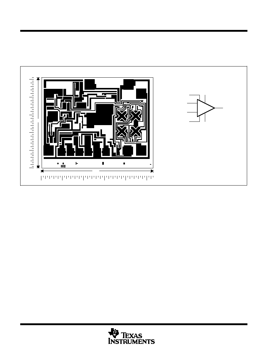
TL061Y chip information
This chip, when properly assembled, has characteristics similar to the TL061. Thermal compression or
ultrasonic bonding can be used on the doped-aluminum bonding pads. The chips can be mounted with
conductive epoxy or a gold-silicon preform.
Bonding-Pad Assignments
+
≠
OUT
IN+
IN≠
VCC+
(7)
(3)
(2)
(6)
(4)
VCC≠
(1)
(5)
OFFSET N1
OFFSET N2
Chip Thickness: 15 Mils Typical
Bonding Pads: 4
◊
4 Mils Minimum
TJ(max) = 150
∞
C
Tolerances Are
±
10%.
All Dimensions Are in Mils.
Pin (4) is Internally Connected
to Backside of Chip.
41
53
(6)
(7)
(8)
(1)
(2)
(3)
(4)
(5)
TL061, TL061A, TL061B, TL061Y, TL062, TL062A
TL062B, TL062Y, TL064, TL064A, TL064B, TL064Y
LOW-POWER JFET-INPUT OPERATIONAL AMPLIFIERS
SLOS078F ≠ NOVEMBER 1978 ≠ REVISED JANUARY 1999
5
POST OFFICE BOX 655303
∑
DALLAS, TEXAS 75265
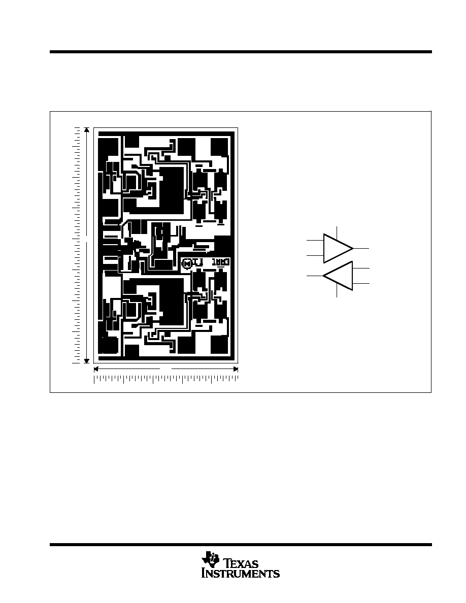
TL062Y chip information
This chip, when properly assembled, has characteristics similar to the TL062. Thermal compression or
ultrasonic bonding can be used on the doped-aluminum bonding pads. The chips can be mounted with
conductive epoxy or a gold-silicon preform.
Bonding-Pad Assignments
Chip Thickness: 15 Mils Typical
Bonding Pads: 4
◊
4 Mils Minimum
TJ(max) = 150
∞
C
Tolerances Are
±
10%.
All Dimensions Are in Mils.
Pin (4) is Internally Connected to Backside of Chip.
+
≠
1OUT
1IN+
1IN≠
VCC+
(8)
(6)
(3)
(2)
(5)
(1)
≠
+
(7)
2IN+
2IN≠
2OUT
(4)
VCC≠
66
49
(6)
(5)
(4)
(3)
(2)
(1)
(8)
(7)