
TL16C550C, TL16C550CI
ASYNCHRONOUS COMMUNICATIONS ELEMENT
WITH AUTOFLOW CONTROL
SLLS177E ≠ MARCH 1994 ≠ REVISED APRIL1998
1
POST OFFICE BOX 655303
∑
DALLAS, TEXAS 75265
D
Programmable Auto-RTS and Auto-CTS
D
In Auto-CTS Mode, CTS Controls
Transmitter
D
In Auto-RTS Mode, RCV FIFO Contents and
Threshold Control RTS
D
Serial and Modem Control Outputs Drive a
RJ11 Cable Directly When Equipment Is on
the Same Power Drop
D
Capable of Running With All Existing
TL16C450 Software
D
After Reset, All Registers Are Identical to
the TL16C450 Register Set
D
Up to 16-MHz Clock Rate for Up to 1-Mbaud
Operation
D
In the TL16C450 Mode, Hold and Shift
Registers Eliminate the Need for Precise
Synchronization Between the CPU and
Serial Data
D
Programmable Baud Rate Generator Allows
Division of Any Input Reference Clock by 1
to (2
16
≠ 1) and Generates an Internal 16
◊
Clock
D
Standard Asynchronous Communication
Bits (Start, Stop, and Parity) Added to or
Deleted From the Serial Data Stream
D
5-V and 3.3-V Operation
D
Independent Receiver Clock Input
D
Transmit, Receive, Line Status, and Data
Set Interrupts Independently Controlled
D
Fully Programmable Serial Interface
Characteristics:
≠ 5-, 6-, 7-, or 8-Bit Characters
≠ Even-, Odd-, or No-Parity Bit Generation
and Detection
≠ 1-, 1 1/2-, or 2-Stop Bit Generation
≠ Baud Generation (dc to 1 Mbit/s)
D
False-Start Bit Detection
D
Complete Status Reporting Capabilities
D
3-State Output TTL Drive Capabilities for
Bidirectional Data Bus and Control Bus
D
Line Break Generation and Detection
D
Internal Diagnostic Capabilities:
≠ Loopback Controls for Communications
Link Fault Isolation
≠ Break, Parity, Overrun, and Framing
Error Simulation
D
Fully Prioritized Interrupt System Controls
D
Modem Control Functions (CTS, RTS, DSR,
DTR, RI, and DCD)
description
The TL16C550C and the TL16C550CI are functional upgrades of the TL16C550B asynchronous
communications element (ACE), which in turn is a functional upgrade of the TL16C450. Functionally equivalent
to the TL16C450 on power up (character or TL16C450 mode), the TL16C550C and the TL16C550CI, like the
TL16C550B, can be placed in an alternate FIFO mode. This relieves the CPU of excessive software overhead
by buffering received and transmitted characters. The receiver and transmitter FIFOs store up to 16 bytes
including three additional bits of error status per byte for the receiver FIFO. In the FIFO mode, there is a
selectable autoflow control feature that can significantly reduce software overload and increase system
efficiency by automatically controlling serial data flow using RTS output and CTS input signals.
The TL16C550C and TL16C550CI perform serial-to-parallel conversions on data received from a peripheral
device or modem and parallel-to-serial conversion on data received from its CPU. The CPU can read the ACE
status at any time. The ACE includes complete modem control capability and a processor interrupt system that
can be tailored to minimize software management of the communications link.
Both the TL16C550C and the TL16C550CI ACE include a programmable baud rate generator capable of
dividing a reference clock by divisors from 1 to 65535 and producing a 16
◊
reference clock for the internal
transmitter logic. Provisions are included to use this 16
◊
clock for the receiver logic. The ACE accommodates
a 1-Mbaud serial rate (16-MHz input clock) so that a bit time is 1
µ
s and a typical character time is 10
µ
s (start
bit, 8 data bits, stop bit).
Two of the TL16C450 terminal functions on the TL16C550C and the TL16C550CI have been changed to
TXRDY and RXRDY, which provide signaling to a DMA controller.
Please be aware that an important notice concerning availability, standard warranty, and use in critical applications of
Texas Instruments semiconductor products and disclaimers thereto appears at the end of this data sheet.
PRODUCTION DATA information is current as of publication date.
Products conform to specifications per the terms of Texas Instruments
standard warranty. Production processing does not necessarily include
testing of all parameters.
Copyright
©
1998, Texas Instruments Incorporated

TL16C550C, TL16C550CI
ASYNCHRONOUS COMMUNICATIONS ELEMENT
WITH AUTOFLOW CONTROL
SLLS177E ≠ MARCH 1994 ≠ REVISED APRIL1998
3
POST OFFICE BOX 655303
∑
DALLAS, TEXAS 75265
detailed description
autoflow control (see Figure 1)
Autoflow control is comprised of auto-CTS and auto-RTS. With auto-CTS, the CTS input must be active before
the transmitter FIFO can emit data. With auto-RTS, RTS becomes active when the receiver needs more data
and notifies the sending serial device. When RTS is connected to CTS, data transmission does not occur unless
the receiver FIFO has space for the data; thus, overrun errors are eliminated using ACE1 and ACE2 from a
TLC16C550C with the autoflow control enabled. If not, overrun errors occur when the transmit data rate exceeds
the receiver FIFO read latency.
RCV
FIFO
Serial to
Parallel
Flow
Control
XMT
FIFO
Parallel
to Serial
Flow
Control
Parallel
to Serial
Flow
Control
Serial to
Parallel
Flow
Control
XMT
FIFO
RCV
FIFO
ACE1
ACE2
D7 ≠ D0
SIN
SOUT
RTS
CTS
SOUT
SIN
CTS
RTS
D7 ≠ D0
Figure 1. Autoflow Control (Auto-RTS and Auto-CTS) Example
auto-RTS (see Figure 1)
Auto-RTS data flow control originates in the receiver timing and control block (see functional block diagram)
and is linked to the programmed receiver FIFO trigger level. When the receiver FIFO level reaches a trigger level
of 1, 4, or 8 (see Figure 3), RTS is deasserted. With trigger levels of 1, 4, and 8, the sending ACE may send
an additional byte after the trigger level is reached (assuming the sending ACE has another byte to send)
because it may not recognize the deassertion of RTS until after it has begun sending the additional byte. RTS
is automatically reasserted once the RCV FIFO is emptied by reading the receiver buffer register.
When the trigger level is 14 (see Figure 4), RTS is deasserted after the first data bit of the 16th character is
present on the SIN line. RTS is reasserted when the RCV FIFO has at least one available byte space.
auto-CTS (see Figure 1)
The transmitter circuitry checks CTS before sending the next data byte. When CTS is active, it sends the next
byte. To stop the transmitter from sending the following byte, CTS must be released before the middle of the
last stop bit that is currently being sent (see Figure 2). The auto-CTS function reduces interrupts to the host
system. When flow control is enabled, CTS level changes do not trigger host interrupts because the device
automatically controls its own transmitter. Without auto-CTS, the transmitter sends any data present in the
transmit FIFO and a receiver overrun error may result.
enabling autoflow control and auto-CTS
Autoflow control is enabled by setting modem control register bits 5 (autoflow enable or AFE) and 1 (RTS) to
a 1. Autoflow incorporates both auto-RTS and auto-CTS. When only auto-CTS is desired, bit 1 in the modem
control register should be cleared (this assumes that a control signal is driving CTS).
TL16C550C, TL16C550CI
ASYNCHRONOUS COMMUNICATIONS ELEMENT
WITH AUTOFLOW CONTROL
SLLS177E ≠ MARCH 1994 ≠ REVISED APRIL1998
4
POST OFFICE BOX 655303
∑
DALLAS, TEXAS 75265
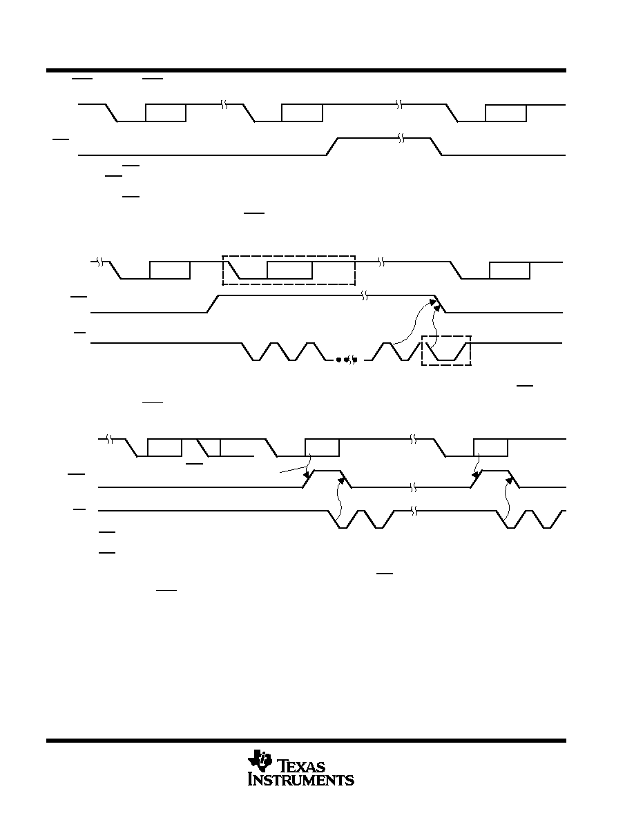
auto-CTS and auto-RTS functional timing
Start
Bits 0 ≠ 7
Start
Bits 0 ≠ 7
Start
Bits 0 ≠ 7
Stop
Stop
Stop
SOUT
CTS
NOTES: A. When CTS is low, the transmitter keeps sending serial data out.
B. If CTS goes high before the middle of the last stop bit of the current byte, the transmitter finishes sending the current byte but it does
not send the next byte.
C. When CTS goes from high to low, the transmitter begins sending data again.
Figure 2. CTS Functional Timing Waveforms
The receiver FIFO trigger level can be set to 1, 4, 8, or 14 bytes. These are described in Figures 3 and 4.
Start
Byte N
Start
Byte N+1
Start
Byte
Stop
Stop
Stop
SIN
RTS
RD
(RD RBR)
1
2
N
N+1
NOTES: A. N = RCV FIFO trigger level (1, 4, or 8 bytes)
B. The two blocks in dashed lines cover the case where an additional byte is sent as described in the preceding auto-RTS section.
Figure 3. RTS Functional Timing Waveforms, RCV FIFO Trigger Level = 1,4, or 8 Bytes
Byte 14
Byte 15
SIN
RTS
RD
(RD RBR)
Start
Byte 18 Stop
Start
Byte 16
Stop
RTS Released After the
First Data Bit of Byte 16
NOTES: A. RTS is deasserted when the receiver receives the first data bit of the sixteenth byte. The receive FIFO is full after finishing the
sixteenth byte.
B. RTS is asserted again when there is at least one byte of space available and no incoming byte is in processing or there is more than
one byte of space available.
C. When the receive FIFO is full, the first receive buffer register read reasserts RTS.
Figure 4. RTS Functional Timing Waveforms, RCV FIFO Trigger Level = 14 Bytes

