
TL16C750
ASYNCHRONOUS COMMUNICATIONS ELEMENT
WITH 64-BYTE FIFOs AND AUTOFLOW CONTROL
SLLS191C ≠ JANUARY 1995 ≠ REVISED DECEMBER 1997
1
POST OFFICE BOX 655303
∑
DALLAS, TEXAS 75265
D
Pin-to-Pin Compatible With the Existing
TL16C550B/C
D
Programmable 16- or 64-Byte FIFOs to
Reduce CPU Interrupts
D
Programmable Auto-RTS and Auto-CTS
D
In Auto-CTS Mode, CTS Controls
Transmitter
D
In Auto-RTS Mode, Receiver FIFO Contents
and Threshold Control RTS
D
Serial and Modem Control Outputs Drive a
RJ11 Cable Directly When Equipment Is on
the Same Power Drop
D
Capable of Running With All Existing
TL16C450 Software
D
After Reset, All Registers Are Identical to
the TL16C450 Register Set
D
Up to 16-MHz Clock Rate for Up to 1-Mbaud
Operation
D
In the TL16C450 Mode, Hold and Shift
Registers Eliminate the Need for Precise
Synchronization Between the CPU and
Serial Data
D
Programmable Baud Rate Generator Allows
Division of Any Input Reference Clock by 1
to (2
16
≠ 1) and Generates an Internal 16
◊
Clock
D
Standard Asynchronous Communication
Bits (Start, Stop, and Parity) Added or
Deleted to or From the Serial Data Stream
D
5-V and 3-V Operation
D
Register Selectable Sleep Mode and
Low-Power Mode
D
Independent Receiver Clock Input
D
Independently Controlled Transmit,
Receive, Line Status, and Data Set
Interrupts
D
Fully Programmable Serial Interface
Characteristics:
≠ 5-, 6-, 7-, or 8-Bit Characters
≠ Even-, Odd-, or No-Parity Bit Generation
and Detection
≠ 1-, 1 1/2-, or 2-Stop Bit Generation
≠ Baud Generation (DC to 1 Mbits Per
Second)
D
False Start Bit Detection
D
Complete Status Reporting Capabilities
D
3-State Output CMOS Drive Capabilities for
Bidirectional Data Bus and Control Bus
D
Line Break Generation and Detection
D
Internal Diagnostic Capabilities:
≠ Loopback Controls for Communications
Link Fault Isolation
≠ Break, Parity, Overrun, Framing Error
Simulation
D
Fully Prioritized Interrupt System Controls
D
Modem Control Functions (CTS, RTS, DSR,
DTR, RI, and DCD)
D
Available in 44-Pin PLCC and 64-Pin SQFP
D
Industrial Temperature Range Available for
64-Pin SQFP
description
The TL16C750 is a functional upgrade of the TL16C550C asynchronous communications element (ACE),
which in turn is a functional upgrade of the TL16C450. Functionally equivalent to the TL16C450 on power up
(character or TL16C450 mode), the TL16C750, like the TL16C550C, can be placed in an alternate mode (FIFO
mode). This relieves the CPU of excessive software overhead by buffering received and transmitted characters.
The receiver and transmitter FIFOs store up to 64 bytes including three additional bits of error status per byte
for the receiver FIFO. The user can choose between a 16-byte FIFO mode or an extended 64-byte FIFO mode.
In the FIFO mode, there is a selectable autoflow control feature that can significantly reduce software overload
and increase system efficiency by automatically controlling serial data flow through the RTS output and the CTS
input signals (see Figure 1).
The TL16C750 performs serial-to-parallel conversion on data received from a peripheral device or modem and
parallel-to-serial conversion on data received from its CPU. The CPU can read the ACE status at any time. The
ACE includes complete modem control capability and a processor interrupt system that can be tailored to
minimize software management of the communications link.
Please be aware that an important notice concerning availability, standard warranty, and use in critical applications of
Texas Instruments semiconductor products and disclaimers thereto appears at the end of this data sheet.
PRODUCTION DATA information is current as of publication date.
Products conform to specifications per the terms of Texas Instruments
standard warranty. Production processing does not necessarily include
testing of all parameters.
Copyright
©
1997, Texas Instruments Incorporated
TL16C750
ASYNCHRONOUS COMMUNICATIONS ELEMENT
WITH 64-BYTE FIFOs AND AUTOFLOW CONTROL
SLLS191C ≠ JANUARY 1995 ≠ REVISED DECEMBER 1997
2
POST OFFICE BOX 655303
∑
DALLAS, TEXAS 75265
description (continued)
The TL16C750 ACE includes a programmable baud rate generator capable of dividing a reference clock by
divisors from 1 to (2
16
≠ 1) and producing a 16
◊
reference clock for the internal transmitter logic. Provisions are
also included to use this 16
◊
clock for the receiver logic. The ACE accommodates a 1-Mbaud serial rate
(16-MHz input clock) so a bit time is 1
µ
s and a typical character time is 10
µ
s (start bit, 8 data bits, stop bit).
Two of the TL16C450 terminal functions have been changed to TXRDY and RXRDY, which provide signaling
to a direct memory access (DMA) controller.
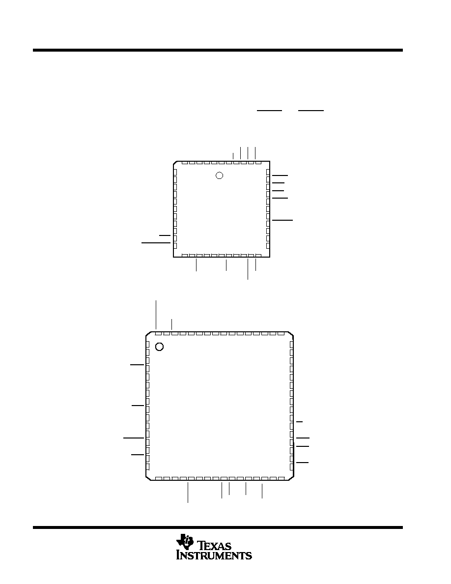
MR
OUT1
DTR
RTS
OUT2
NC
INTRPT
RXRDY
A0
A1
A2
39
38
37
36
35
34
33
32
31
30
29
18 19
7
8
9
10
11
12
13
14
15
16
17
D5
D6
D7
RCLK
SIN
NC
SOUT
CS0
CS1
CS2
BAUDOUT
20 21 22 23
RI
DCD
DSR
CTS
5 4 3
2 1
6
44
D4
D3
D2
D1
D0
NC
V
RD2
DDIS
TXRDY
ADS
XIN
XOUT
WR1
WR2
NC
RD1
42 41 40
43
24 25 26 27 28
NC ≠ No internal connection
CC
V
SS
FN PACKAGE
(TOP VIEW)
18 19
D4
NC
D3
D2
NC
D1
D0
NC
VCC
NC
RI
NC
DCD
DSR
NC
CTS
48
47
46
45
44
43
42
41
40
39
38
37
36
35
34
33
20
1
2
3
4
5
6
7
8
9
10
11
12
13
14
15
16
XIN
XOUT
NC
WR1
NC
WR2
NC
VSS
RD1
RD2
NC
DDIS
TXRDY
NC
ADS
NC
21 22 23 24
PM PACKAGE
(TOP VIEW)
D6
SIN
63 62 61 60 59
64
58
CS2
NC
CS1
NC
CS0
SOUT
NC
RT
S
NC
DTR
NC
NC
A0
RXRDY
NC
INTRPT
NC
OUT2
56 55 54
57
25 26 27 28 29
53 52
17
A2
RCLK
NC
51 50 49
30 31 32
OUT1
NC
MR
D7
NC
D5
BAUDOUT
NC
A1

TL16C750
ASYNCHRONOUS COMMUNICATIONS ELEMENT
WITH 64-BYTE FIFOs AND AUTOFLOW CONTROL
SLLS191C ≠ JANUARY 1995 ≠ REVISED DECEMBER 1997
3
POST OFFICE BOX 655303
∑
DALLAS, TEXAS 75265
functional block diagram
Receiver
Buffer
Register
Divisor
Latch (LS)
Divisor
Latch (MS)
Baud
Generator
Receiver
FIFO
Line
Status
Register
Transmitter
Holding
Register
Modem
Control
Register
Modem
Status
Register
Line
Control
Register
Transmitter
FIFO
Interrupt
Enable
Register
Interrupt
Identification
Register
FIFO
Control
Register
Select
and
Control
Logic
Interrupt
Control
Logic
S
e
l
e
c
t
Data
Bus
Buffer
BAUDOUT
SIN
RCLK
SOUT
CTS
DTR
DSR
DCD
RI
OUT1
OUT2
INTRPT
40
37
41
42
43
38
35
33
13
10
11
17
14
A0
31
D(7 ≠ 0)
9 ≠ 2
Internal
Data Bus
30
29
15
16
28
39
24
25
20
21
26
27
18
19
32
A1
A2
CS0
CS1
CS2
ADS
MR
RD1
RD2
WR1
WR2
DDIS
TXRDY
XIN
XOUT
RXRDY
S
e
l
e
c
t
Receiver
Shift
Register
Receiver
Timing and
Control
Transmitter
Timing and
Control
Transmitter
Shift
Register
Modem
Control
Logic
8
44
22
VCC
VSS
Power
Supply
RTS
36
Autoflow
Control
Enable
(AFE)
8
8
8
8
8
8
8
NOTE A: Terminal numbers shown are for the FN package.

TL16C750
ASYNCHRONOUS COMMUNICATIONS ELEMENT
WITH 64-BYTE FIFOs AND AUTOFLOW CONTROL
SLLS191C ≠ JANUARY 1995 ≠ REVISED DECEMBER 1997
4
POST OFFICE BOX 655303
∑
DALLAS, TEXAS 75265
Terminal Functions
TERMINAL
NAME
NO.
FN
NO.
PM
I/O
DESCRIPTION
A0
A1
A2
31
30
29
20
18
17
I
Register select. A0 ≠ A2 are used during read and write operations to select the ACE register to read from
or write to. Refer to Table 1 for register addresses and ADS signal description.
ADS
28
15
I
Address strobe. When ADS is active (low), the register select signals (A0, A1, and A2) and chip select signals
(CS0, CS1, CS2) drive the internal select logic directly; when ADS is high, the register select and chip select
signals are held at the logic levels they were in when the low-to-high transition of ADS occurred.
BAUDOUT
17
64
O
Baud out. BAUDOUT is a 16
◊
clock signal for the transmitter section of the ACE. The clock rate is established
by the reference oscillator frequency divided by a divisor specified by the baud generator divisor latches.
BAUDOUT can also be used for the receiver section by tying this output to RCLK.
CS0
CS1
CS2
14
15
16
59
61
62
I
Chip select. When CS0 and CS1 are high and CS2 is low, the ACE is selected. When any of these inputs
are inactive, the ACE remains inactive. Refer to the ADS signal description.
CTS
40
33
I
Clear to send. CTS is a modem status signal. Its condition can be checked by reading bit 4 (CTS) of the
modem status register. Bit 0 (
CTS) of the modem status register indicates that CTS has changed states
since the last read from the modem status register. When the modem status interrupt is enabled, CTS
changes states, and the auto-CTS mode is not enabled, an interrupt is generated. CTS is also used in the
auto-CTS mode to control the transmitter.
D0
D1
D2
D3
D4
D5
D6
D7
2
3
4
5
6
7
8
9
42
43
45
46
48
50
51
52
I/O
Data bus. Eight data lines with 3-state outputs provide a bidirectional path for data, control, and status
information between the ACE and the CPU. As inputs, they use fail safe CMOS compatible input buffers.
DCD
42
36
I
Data carrier detect. DCD is a modem status signal. Its condition can be checked by reading bit 7 (DCD) of
the modem status register. Bit 3 (
DCD) of the modem status register indicates that DCD has changed states
since the last read from the modem status register. When the modem status interrupt is enabled and DCD
changes state, an interrupt is generated.
DDIS
26
12
O
Driver disable. DDIS is active (high) when the CPU is not reading data. When active, DDIS can disable an
external transceiver.
DSR
41
35
I
Data set ready. DSR is a modem status signal. Its condition can be checked by reading bit 5 (DSR) of the
modem status register. Bit 1 (
DSR) of the modem status register indicates DSR has changed states since
the last read from the modem status register. When the modem status interrupt is enabled and the DSR
changes states, an interrupt is generated.
DTR
37
28
O
Data terminal ready. When active (low), DTR informs a modem or data set that the ACE is ready to establish
communication. DTR is placed in the active state by setting the DTR bit of the modem control register to one.
DTR is placed in the inactive condition either as a result of a master reset, during loop mode operation, or
clearing the DTR bit.
INTRPT
33
23
O
Interrupt. When active (high), INTRPT informs the CPU that the ACE has an interrupt to be serviced. Four
conditions that cause an interrupt to be issued are: a receiver error, received data that is available or timed
out (FIFO mode only), an empty transmitter holding register, or an enabled modem status interrupt. INTRPT
is reset (deactivated) either when the interrupt is serviced or as a result of a master reset.
MR
39
32
I
Master reset. When active (high), MR clears most ACE registers and sets the levels of various output signals
(refer to Table 2).
OUT1
OUT2
38
35
30
25
O
Outputs 1 and 2. These are user-designated output terminals that are set to their active (low) level by setting
their respective modem control register (MCR) bits (OUT1 and OUT2). OUT1 and OUT2 are set to their
inactive (high) level as a result of master reset, during loop mode operations, or by clearing bit 2 (OUT1) or
bit 3 (OUT2) of the MCR.
RCLK
10
54
I
Receiver clock. RCLK is the 16
◊
baud rate clock for the receiver section of the ACE.

TL16C750
ASYNCHRONOUS COMMUNICATIONS ELEMENT
WITH 64-BYTE FIFOs AND AUTOFLOW CONTROL
SLLS191C ≠ JANUARY 1995 ≠ REVISED DECEMBER 1997
5
POST OFFICE BOX 655303
∑
DALLAS, TEXAS 75265
Terminal Functions (Continued)
TERMINAL
NAME
NO.
FN
NO.
PM
I/O
DESCRIPTION
RD1
RD2
24
25
9
10
I
Read inputs. When either RD1 or RD2 is active (low or high respectively) while the ACE is selected, the CPU
is allowed to read status information or data from a selected ACE register. Only one of these inputs is required
for the transfer of data during a read operation; the other input should be tied in its inactive state (i.e., RD2 tied
low or RD1 tied high).
RI
43
38
I
Ring indicator. RI is a modem status signal. Its condition can be checked by reading bit 6 (RI) of the modem
status register. Bit 2 (TERI) of the modem status register indicates that RI has transitioned from a low to a high
level since the last read from the modem status register. If the modem status interrupt is enabled when this
transition occurs, an interrupt is generated.
RTS
36
26
O
Request to send. When active, RTS informs the modem or data set that the ACE is ready to receive data. RTS
is set to its active level by setting the RTS MCR bit and is set to its inactive (high) level either as a result of a
master reset, during loop mode operations, or by clearing bit 1 (RTS) of the MCR. In the auto-RTS mode, RTS
is set to its inactive level by the receiver threshold control logic.
RXRDY
32
21
O
Receiver ready. Receiver direct memory access (DMA) signalling is available with RXRDY. When operating
in the FIFO mode, one of two types of DMA signalling can be selected through the FIFO control register bit
3 (FCR3). When operating in the TL16C450 mode, only DMA mode 0 is allowed. Mode 0 supports
single-transfer DMA in which a transfer is made between CPU bus cycles. Mode 1 supports multitransfer DMA
in which multiple transfers are made continuously until the receiver FIFO has been emptied. In DMA mode 0
(FCR0 = 0 or FCR0 = 1, FCR3 = 0), when there is at least one character in the receiver FIFO or receiver holding
register, RXRDY is active (low). When RXRDY has been active but there are no characters in the FIFO or
holding register, RXRDY goes inactive (high). In DMA mode 1 (FCR0 = 1, FCR3 = 1), when the trigger level
or the timeout has been reached, RXRDY goes active (low); when it has been active but there are no more
characters in the FIFO or holding register, it goes inactive (high).
SIN
11
55
I
Serial data. SIN is the input from a connected communications device.
SOUT
13
58
O
Composite serial data output to a connected communication device. SOUT is set to the marking (high) level
as a result of master reset.
TXRDY
27
13
O
Transmitter ready. Transmitter DMA signalling is available with TXRDY. When operating in the FIFO mode,
one of two types of DMA signalling can be selected through FCR3. When operating in the TL16C450 mode,
only DMA mode 0 is allowed. Mode 0 supports single-transfer DMA in which a transfer is made between CPU
bus cycles. Mode 1 supports multitransfer DMA in which multiple transfers are made continuously until the
transmit FIFO has been filled.
VCC
44
40
5-V supply voltage
VSS
22
8
Supply common
WR1
WR2
20
21
4
6
I
Write inputs. When either input is active (low or high respectively) and while the ACE is selected, the CPU is
allowed to write control words or data into a selected ACE register. Only one of these inputs is required to
transfer data during a write operation; the other input should be tied in its inactive state (i.e., WR2 tied low or
WR1 tied high).
XIN
XOUT
18
19
1
2
I/O
External clock. XIN and XOUT connect the ACE to the main timing reference (clock or crystal).
detailed description
autoflow control
Auto-flow control is composed of auto-CTS and auto-RTS. With auto-CTS, CTS must be active before the
transmit FIFO can emit data (see Figure 1). With auto-RTS, RTS becomes active when the receiver is empty
or the threshold has not been reached. When RTS is connected to CTS, data transmission does not occur
unless the receive FIFO has empty space. Thus, overrun errors are eliminated when ACE1 and ACE2 are
TLC16C750s with enabled autoflow control. If not, overrun errors occur if the transmit data rate exceeds the
receive FIFO read latency.