 | –≠–ª–µ–∫—Ç—Ä–æ–Ω–Ω—ã–π –∫–æ–º–ø–æ–Ω–µ–Ω—Ç: TL431AID | –°–∫–∞—á–∞—Ç—å:  PDF PDF  ZIP ZIP |

TL431, TL431A
ADJUSTABLE PRECISION SHUNT REGULATORS
SLVS005J ≠ JULY 1978 ≠ REVISED JULY 1999
1
POST OFFICE BOX 655303
∑
DALLAS, TEXAS 75265
D
Equivalent Full-Range Temperature
Coefficient . . . 30 ppm/
∞
C
D
0.2-
Typical Output Impedance
D
Sink-Current Capability . . . 1 mA to 100 mA
D
Low Output Noise
D
Adjustable Output Voltage . . . V
ref
to 36 V
D
Available in a Wide Range of High-Density
Packages
description
The TL431 and TL431A are three-terminal
adjustable shunt regulators with specified thermal
stability over applicable automotive, commercial,
and military temperature ranges. The output
voltage can be set to any value between V
ref
(approximately 2.5 V) and 36 V with two external
resistors (see Figure 17). These devices have a
typical output impedance of 0.2
. Active output
circuitry provides a very sharp turn-on
characteristic, making these devices excellent
replacements for Zener diodes in many
applications, such as onboard regulation,
adjustable power supplies, and switching power
supplies.
The TL431C and TL431AC are characterized for
operation from 0
∞
C to 70
∞
C, and the TL431I and
TL431AI are characterized for operation from
≠40
∞
C to 85
∞
C.
Please be aware that an important notice concerning availability, standard warranty, and use in critical applications of
Texas Instruments semiconductor products and disclaimers thereto appears at the end of this data sheet.
1
2
3
4
8
7
6
5
CATHODE
ANODE
ANODE
NC
REF
ANODE
ANODE
NC
D PACKAGE
(TOP VIEW)
1
2
3
4
8
7
6
5
CATHODE
NC
NC
NC
REF
NC
ANODE
NC
P OR PW PACKAGE
(TOP VIEW)
PK PACKAGE
(TOP VIEW)
LP PACKAGE
(TOP VIEW)
REF ANODE CATHODE
CATHODE
ANODE
REF
CATHODE
ANODE
REF
ANODE
KTP PACKAGE
(TOP VIEW)
NC ≠ No internal connection
PRODUCTION DATA information is current as of publication date.
Products conform to specifications per the terms of Texas Instruments
standard warranty. Production processing does not necessarily include
testing of all parameters.
Copyright
©
1999, Texas Instruments Incorporated

TL431, TL431A
ADJUSTABLE PRECISION SHUNT REGULATORS
SLVS005J ≠ JULY 1978 ≠ REVISED JULY 1999
2
POST OFFICE BOX 655303
∑
DALLAS, TEXAS 75265
AVAILABLE OPTIONS
PACKAGED DEVICES
TA
SMALL
OUTLINE
(D)
PLASTIC
FLANGE
MOUNT
(KTP)
TO-226AA
(LP)
PLASTIC
DIP
(P)
SOT-89
(PK)
SHRINK
SMALL
OUTLINE
(PW)
CHIP
FORM
(Y)
0
∞
C to 70
∞
C
TL431CD
TL431ACD
TL431CKTPR
TL431CLP
TL431ACLP
TL431CP
TL431ACP
TL431CPK
TL431CPW
TL431Y
≠40
∞
C to 85
∞
C
TL431ID
TL431AID
TL431ILP
TL431AILP
TL431IP
TL431AIP
TL431IPK
TL431Y
The D and LP packages are available taped and reeled. The KTP and PK packages are only available taped and reeled. Add
the suffix R to device type (e.g., TL431CDR). Chip forms are tested at TA = 25
∞
C.
symbol
REF
CATHODE
ANODE
functional block diagram
CATHODE
REF
ANODE
+
_
Vref
equivalent schematic
ANODE
REF
CATHODE
2.4 k
7.2 k
3.28 k
20 pF
4 k
1 k
800
800
800
20 pF
150
10 k
All component values are nominal.

TL431, TL431A
ADJUSTABLE PRECISION SHUNT REGULATORS
SLVS005J ≠ JULY 1978 ≠ REVISED JULY 1999
3
POST OFFICE BOX 655303
∑
DALLAS, TEXAS 75265
absolute maximum ratings over operating free-air temperature range (unless otherwise noted)
Cathode voltage, V
KA
(see Note 1)
37 V
. . . . . . . . . . . . . . . . . . . . . . . . . . . . . . . . . . . . . . . . . . . . . . . . . . . . . . . . . . .
Continuous cathode current range, I
KA
≠100 mA to 150 mA
. . . . . . . . . . . . . . . . . . . . . . . . . . . . . . . . . . . . . . . . .
Reference input current range
≠50
µ
A to 10 mA
. . . . . . . . . . . . . . . . . . . . . . . . . . . . . . . . . . . . . . . . . . . . . . . . . . . .
Package thermal impedance,
JA
(see Notes 2 and 3): D package
97
∞
C/W
. . . . . . . . . . . . . . . . . . . . . . . . . . . .
LP package
156
∞
C/W
. . . . . . . . . . . . . . . . . . . . . . . . . .
KTP package
28
∞
C/W
. . . . . . . . . . . . . . . . . . . . . . . . .
P package
127
∞
C/W
. . . . . . . . . . . . . . . . . . . . . . . . . . . .
PK package
52
∞
C/W
. . . . . . . . . . . . . . . . . . . . . . . . . . .
PW package
149
∞
C/W
. . . . . . . . . . . . . . . . . . . . . . . . . .
Lead temperature 1,6 mm (1/16 inch) from case for 10 seconds: D, P, or PW package
260
∞
C
. . . . . . . . . . . .
Lead temperature 1,6 mm (1/16 inch) from case for 60 seconds: LP or PK package
300
∞
C
. . . . . . . . . . . . . .
Storage temperature range, T
stg
≠65
∞
C to 150
∞
C
. . . . . . . . . . . . . . . . . . . . . . . . . . . . . . . . . . . . . . . . . . . . . . . . . . .
Stresses beyond those listed under "absolute maximum ratings" may cause permanent damage to the device. These are stress ratings only, and
functional operation of the device at these or any other conditions beyond those indicated under "recommended operating conditions" is not
implied. Exposure to absolute-maximum-rated conditions for extended periods may affect device reliability.
NOTES:
1. Voltage values are with respect to the anode terminal unless otherwise noted.
2. Maximum power dissipation is a function of TJ(max),
JA, and TA. The maximum allowable power dissipation at any allowable
ambient temperature is PD = (TJ(max) ≠ TA)/
JA. Operating at the absolute maximum TJ of 150
∞
C can impact reliability.
3. The package thermal impedance is calculated in accordance with JESD 51, except for through-hole packages, which use a trace
length of zero.
recommended operating conditions
MIN
MAX
UNIT
Cathode voltage, VKA
Vref
36
V
Cathode current, IKA
1
100
mA
Operating free air temperature range TA
TL431C, TL431AC
0
70
∞
C
Operating free-air temperature range, TA
TL431I, TL431AI
≠40
85
∞
C
TL431, TL431A
ADJUSTABLE PRECISION SHUNT REGULATORS
SLVS005J ≠ JULY 1978 ≠ REVISED JULY 1999
4
POST OFFICE BOX 655303
∑
DALLAS, TEXAS 75265
electrical characteristics over recommended operating conditions, T
A
= 25
∞
C (unless otherwise
noted)
PARAMETER
TEST
TEST CONDITIONS
TL431C
UNIT
PARAMETER
CIRCUIT
TEST CONDITIONS
MIN
TYP
MAX
UNIT
Vref
Reference voltage
2
VKA = Vref,
IKA = 10 mA
2440
2495
2550
mV
VI(dev)
Deviation of reference voltage
over full temperature range
(see Figure 1)
2
VKA = Vref, IKA = 10 mA,
TA = full range
4
25
mV
D
V
ref
Ratio of change in reference voltage
3
IKA = 10 mA
VKA = 10 V ≠ Vref
≠1.4
≠2.7
mV
ref
D
V
KA
g
g
to the change in cathode voltage
3
IKA = 10 mA
VKA = 36 V ≠ 10 V
≠1
≠2
mV
V
Iref
Reference current
3
IKA = 10 mA, R1 = 10 k
, R2 =
2
4
µ
A
II(dev)
Deviation of reference current
over full temperature range
(see Figure 1)
3
IKA = 10 mA, R1 = 10 k
, R2 =
,
TA = full range
0.4
1.2
µ
A
Imin
Minimum cathode current
for regulation
2
VKA = Vref
0.4
1
mA
Ioff
Off-state cathode current
4
VKA = 36 V,
Vref = 0
0.1
1
µ
A
|zKA|
Dynamic impedance (see Figure 1)
1
IKA = 1 mA to 100 mA, VKA = Vref,
f
1 kHz
0.2
0.5
Full range is 0
∞
C to 70
∞
C for the TL431C.
The deviation parameters V
ref(dev)
and I
ref(dev)
are defined as the differences between the maximum and minimum
values obtained over the recommended temperature range. The average full-range temperature coefficient of the
reference voltage,
Vref
, is defined as:
where:
T
A
is the recommended operating free-air temperature range of the device.
Vref
can be positive or negative, depending on whether minimum V
ref
or maximum V
ref
, respectively, occurs at the
lower temperature.
Example: maximum V
ref
= 2496 mV at 30
∞
C, minimum V
ref
= 2492 mV at 0
∞
C, V
ref
= 2495 mV at 25
∞
C,
T
A
= 70
∞
C for TL431C
Because minimum V
ref
occurs at the lower temperature, the coefficient is positive.
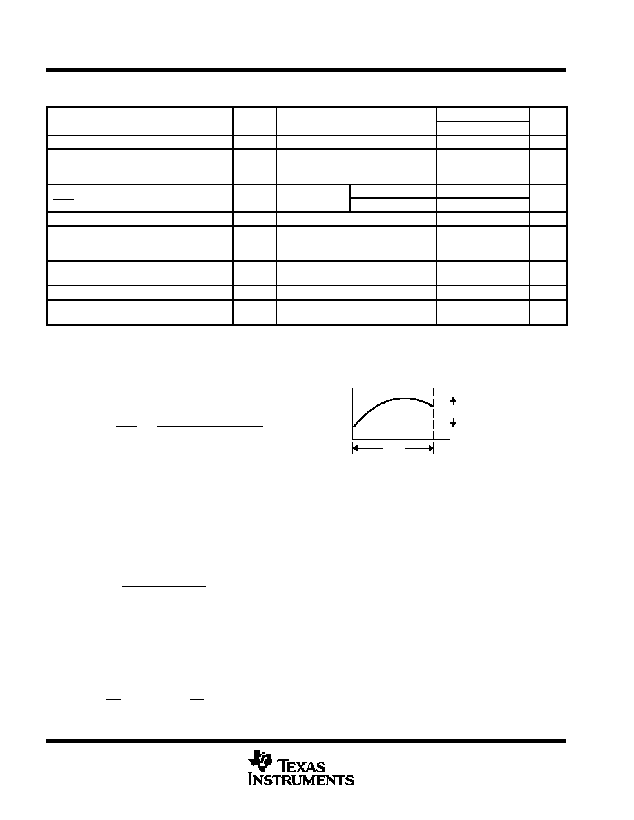
Calculating Dynamic Impedance
The dynamic impedance is defined as:
When the device is operating with two external resistors (see Figure 3), the total dynamic impedance of the circuit
is given by:
Maximum Vref
Minimum Vref
TA
VI(dev)
a
Vref
ppm
∞
C
+
V
I(dev)
V
ref
at 25
∞
C
106
D
T
A
a
Vref
+
4 mV
2495 mV
106
70
∞
C
[
23 ppm
∞
C
z
KA
+
D
V
KA
D
I
KA
|z |
+ D
V
D
I
[
z
KA
1
)
R1
R2
Figure 1. Calculating Deviation Parameters and Dynamic Impedance

TL431, TL431A
ADJUSTABLE PRECISION SHUNT REGULATORS
SLVS005J ≠ JULY 1978 ≠ REVISED JULY 1999
5
POST OFFICE BOX 655303
∑
DALLAS, TEXAS 75265
electrical characteristics over recommended operating conditions, T
A
= 25
∞
C (unless otherwise
noted)
PARAMETER
TEST
TEST CONDITIONS
TL431I
UNIT
PARAMETER
CIRCUIT
TEST CONDITIONS
MIN
TYP
MAX
UNIT
Vref
Reference voltage
2
VKA = Vref,
IKA = 10 mA
2440
2495
2550
mV
VI(dev)
Deviation of reference voltage
over full temperature range
(see Figure 1)
2
VKA = Vref, IKA = 10 mA,
TA = full range
5
50
mV
D
V
ref
Ratio of change in reference voltage
3
IKA = 10 mA
VKA = 10 V ≠ Vref
≠1.4
≠2.7
mV
ref
D
V
KA
g
g
to the change in cathode voltage
3
IKA = 10 mA
VKA = 36 V ≠ 10 V
≠1
≠2
mV
V
Iref
Reference current
3
IKA = 10 mA, R1 = 10 k
, R2 =
2
4
µ
A
II(dev)
Deviation of reference current
over full temperature range
(see Figure 1)
3
IKA = 10 mA, R1 = 10 k
, R2 =
,
TA = full range
0.8
2.5
µ
A
Imin
Minimum cathode current for
regulation
2
VKA = Vref
0.4
1
mA
Ioff
Off-state cathode current
4
VKA = 36 V,
Vref = 0
0.1
1
µ
A
|zKA|
Dynamic impedance (see Figure 1)
2
IKA = 1 mA to 100 mA, VKA = Vref,
f
1 kHz
0.2
0.5
Full range is ≠40
∞
C to 85
∞
C for the TL431I.
electrical characteristics over recommended operating conditions, T
A
= 25
∞
C (unless otherwise
noted)
PARAMETER
TEST
TEST CONDITIONS
TL431AC
UNIT
PARAMETER
CIRCUIT
TEST CONDITIONS
MIN
TYP
MAX
UNIT
Vref
Reference voltage
2
VKA = Vref,
IKA = 10 mA
2470
2495
2520
mV
VI(dev)
Deviation of reference voltage
over full temperature range
(see Figure 1)
2
VKA = Vref, IKA = 10 mA,
TA = full range
4
25
mV
D
V
ref
Ratio of change in reference voltage
3
IKA = 10 mA
VKA = 10 V ≠ Vref
≠1.4
≠2.7
mV
ref
D
V
KA
g
g
to the change in cathode voltage
3
IKA = 10 mA
VKA = 36 V ≠ 10 V
≠1
≠2
mV
V
Iref
Reference current
3
IKA = 10 mA, R1 = 10 k
, R2 =
2
4
µ
A
II(dev)
Deviation of reference current
over full temperature range
(see Figure 1)
3
IKA = 10 mA, R1 = 10 k
, R2 =
,
TA = full range
0.8
1.2
µ
A
Imin
Minimum cathode current
for regulation
2
VKA = Vref
0.4
0.6
mA
Ioff
Off-state cathode current
4
VKA = 36 V,
Vref = 0
0.1
0.5
µ
A
|zKA|
Dynamic impedance (see Figure 1)
1
IKA = 1 mA to 100 mA, VKA = Vref,
f
1 kHz
0.2
0.5
Full range is 0
∞
C to 70
∞
C for the TL431AC.