 | –≠–ª–µ–∫—Ç—Ä–æ–Ω–Ω—ã–π –∫–æ–º–ø–æ–Ω–µ–Ω—Ç: TLC2551 | –°–∫–∞—á–∞—Ç—å:  PDF PDF  ZIP ZIP |
TLC2551, TLC2552, TLC2555
5 V, LOW POWER, 12-BIT, 400 KSPS,
SERIAL ANALOG-TO-DIGITAL CONVERTERS WITH AUTOPOWER DOWN
SLAS276 ≠MARCH 2000
1
POST OFFICE BOX 655303
∑
DALLAS, TEXAS 75265
D
Maximum Throughput . . . 400 KSPS
D
INL/DNL:
±
1 LSB Max, SINAD: 72 dB,
f
i
= 20 kHz, SFDR: 85 dB, f
i
= 20 kHz
D
SPI/DSP-Compatible Serial Interfaces With
SCLK up to 20 MHz
D
Single 5 V Supply
D
Rail-to-Rail Analog Input With 500 kHz BW
D
Three Options Available:
≠ TLC2551 ≠ Single Channel Input
≠ TLC2552 ≠ Dual Channels With
Autosweep
≠ TLC2555 ≠ Single Channel With
Pseudo-Differential Input
D
Optimized DSP Mode ≠ Requires FS Only
D
Low Power With Autopower Down
≠ Operating Current : 3.5 mA
Autopower Down: 8
µ
A
D
Small 8-Pin MSOP and SOIC Packages
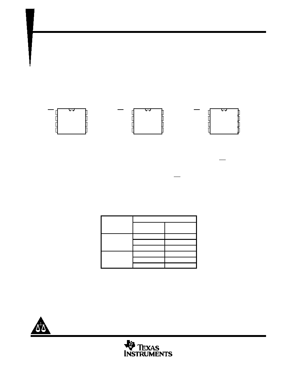
PACKAGE TOP VIEW
TLC2551
1
2
3
4
8
7
6
5
CS
V
REF
GND
AIN
SDO
FS
V
DD
SCLK
1
2
3
4
8
7
6
5
CS/FS
V
REF
GND
AIN0
SDO
SCLK
V
DD
AIN1
TLC2552
1
2
3
4
8
7
6
5
CS/FS
V
REF
GND
AIN(+)
SDO
SCLK
V
DD
AIN(≠)
TLC2555
description
The TLC2551/2552/2555 are a family of high performance, 12-bit, low power, miniature 1.5
µ
s, CMOS
analog-to-digital converters (ADC). The TLC255x family uses a 5 V supply. Devices are available with single,
dual, or single pseudo-differential inputs. The TLC2551 has a 3-state output chip select (CS), serial output clock
(SCLK), and serial data output (SDO) that provides a direct 3-wire interface to the serial port of most popular
host microprocessors (SPI interface). When interfaced with a DSP, a frame sync signal (FS) is used to indicate
the start of a serial data frame. The TLV2552/55 have a shared CS/FS terminal.
TLC2551/2/5 are designed to operate with very low power consumption. The power saving feature is further
enhanced with an autopower-down mode. This product family features a high-speed serial link to modern host
processors with SCLK up to 20 MHz. TLC255x family uses the SCLK as the conversion clock, thus providing
synchronous operation allowing a minimum conversion time of 1.5
µ
s using 20 MHz SCLK.
AVAILABLE OPTIONS
PACKAGED DEVICES
TA
8-MSOP
(DGK)
8-SOIC
(D)
TLC2551CDGK
0
∞
C to 70
∞
C
TLC2552CDGK
TLC2555CDGK
TLC2551IDGK
TLC2551ID
≠ 40
∞
C to 85
∞
C
TLC2552IDGK
TLC2552ID
TLC2555IDGK
TLC2555ID
Copyright
©
2000, Texas Instruments Incorporated
PRODUCTION DATA information is current as of publication date.
Products conform to specifications per the terms of Texas Instruments
standard warranty. Production processing does not necessarily include
testing of all parameters.
Please be aware that an important notice concerning availability, standard warranty, and use in critical applications of
Texas Instruments semiconductor products and disclaimers thereto appears at the end of this data sheet.

TLC2551, TLC2552, TLC2555
5 V, LOW POWER, 12-BIT, 400 KSPS,
SERIAL ANALOG-TO-DIGITAL CONVERTERS WITH AUTOPOWER DOWN
SLAS276 ≠MARCH 2000
2
POST OFFICE BOX 655303
∑
DALLAS, TEXAS 75265
functional block diagram
S/H
SDO
REF
LOW POWER
SAR ADC
VDD
Conversion
Clock
CONTROL
LOGIC
Mux
S/H
LOW POWER
12-BIT
SAR ADC
Conversion
Clock
CONTROL
LOGIC
AIN
SCLK
CS
FS
REF
AIN0
AIN1
SCLK
CS/FS
SDO
VDD
GND
GND
TLC2551
TLC2552
S/H
LOW POWER
12-BIT
SAR ADC
Conversion
Clock
CONTROL
LOGIC
REF
AIN (+)
AIN (≠)
SCLK
CS/FS
SDO
VDD
GND
TLC2555

TLC2551, TLC2552, TLC2555
5 V, LOW POWER, 12-BIT, 400 KSPS,
SERIAL ANALOG-TO-DIGITAL CONVERTERS WITH AUTOPOWER DOWN
SLAS276 ≠MARCH 2000
3
POST OFFICE BOX 655303
∑
DALLAS, TEXAS 75265
Terminal Functions
TLC2551
TERMINAL
I/O
DESCRIPTION
NAME
NO.
I/O
DESCRIPTION
AIN
4
I
Analog input channel
CS
1
I
Chip select. A high-to-low transition on the CS input removes SDO from 3-state within a maximum setup time.
CS can be used as the FS pin when a dedicated serial port is used. If TLC2551 is attached to a dedicated DSP serial
port, this terminal can be grounded.
FS
7
I
DSP frame sync input. Indication of the start of a serial data frame. Tie this terminal to VDD if not used.
GND
3
I
Ground return for the internal circuitry. Unless otherwise noted, all voltage measurements are with respect to GND.
SCLK
5
I
Output serial clock. This terminal receives the serial SCLK from the host processor.
SDO
8
O
The 3-state serial output for the A/D conversion result. SDO is kept in the high-impedance state until CS falling edge.
The output format is MSB first.
When FS is not used (FS = 1 at the falling edge of CS): The MSB is presented to the SDO pin after CS falling edge
and output data is valid on the falling edge of SCLK.
When FS is used (FS = 0 at the falling edge of CS): The MSB is presented to the SDO pin after the falling edge of
FS or the falling edge of CS (whichever happens first). Output data is valid on the falling edge of SCLK. (This is
typically used with an active FS from a DSP).
VDD
6
I
Positive supply voltage
VREF
2
I
External reference input
TLC2552/55
TERMINAL
I/O
DESCRIPTION
NAME
NO.
I/O
DESCRIPTION
AIN0 /AIN(+)
4
I
Analog input channel 0. (positive input for TLV2555)
AIN1/AIN (≠)
5
I
Analog input channel 1 (inverted input for TLV2555)
CS/FS
1
I
Chip select/frame sync. A high-to-low transition on the CS/FS removes SDO from 3-state within a maximum delay
time.
GND
3
I
Ground return for the internal circuitry. Unless otherwise noted, all voltage measurements are with respect to GND.
SCLK
7
I
Output serial clock. This terminal receives the serial SCLK from the host processor.
SDO
8
O
The 3-state serial output for the A/D conversion result. SDO is kept in the high-impedance state when CS/FS is
high and presents output data after the CS/FS falling edge until the LSB is presented. The output format is MSB
first. SDO returns to the Hi-Z state after the 16th SCLK. Output data is valid on the falling SCLK edge.
VDD
6
I
Positive supply voltage
VREF
2
I
External reference input
detailed description
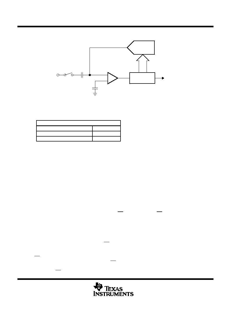
The TLC2551/2/5 are successive approximation (SAR) ADCs utilizing a charge redistribution DAC. Figure 1
shows a simplified version of the ADC.
The sampling capacitor acquires the signal on AIN during the sampling period. When the conversion process
starts, the SAR control logic and charge redistribution DAC are used to add and subtract fixed amounts of charge
from the sampling capacitor to bring the comparator into a balanced condition. When the comparator is
balanced, the conversion is complete and the ADC output code is generated.
TLC2551, TLC2552, TLC2555
5 V, LOW POWER, 12-BIT, 400 KSPS,
SERIAL ANALOG-TO-DIGITAL CONVERTERS WITH AUTOPOWER DOWN
SLAS276 ≠MARCH 2000
4
POST OFFICE BOX 655303
∑
DALLAS, TEXAS 75265
detailed description (continued)
GND/AIN(≠)
ADC Code
AIN
Charge
Redistribution
DAC
Control
Logic
_
+
Figure 1. Simplified SAR Circuit
serial interface
OUTPUT DATA FORMAT
MSB
LSB
D15≠D4
D3≠D0
Conversion result (OD11≠OD0)
Don't care
The output data format is binary (unipolar straight binary).
binary
Zero scale code = 000h, Vcode = GND
Full scale code = FFFh, Vcode = VREFP ≠ 1 LSB
pseudo-differential inputs
The TLC2555 operates in pseudo-differential mode. The inverted input is available on terminal 5. It can have
a maximum input ripple of
±
0.2 V. This is normally used for ground noise rejection.
control and timing
start of the cycle
TLC2551
D
When FS is not used ( FS = 1 at the falling edge of CS), the falling edge of CS is the start of the cycle. Output
data changes on the rising edge of SCLK. This is typically used for a microcontroller with SPI interface,
although it can also be used for a DSP. The microcontroller SPI interface should be programmed for
CPOL=0 (serial clock reference to ground) and CPHA=1 (data is valid on the falling edge of serial clock).
D
When FS is used ( FS is an active signal from a DSP), the falling edge of FS is the start of the cycle. Output
data changes on the rising edge of SCLK. This is typically used for a TMS320 DSP. If the TLC2551 is
attached to a dedicated DSP serial port. CS terminal can be grounded.
TLC2552/5
The CS and FS inputs are accessed via the same pin (pin 1) on the TLC2552 and TLC2555. The cycle is started
by the falling edge transition provided by either a CS (interfacing with a SPI interface microcontroller) signal or
FS (interfacing with a TMS320 DSP) signal. Timing for the TLC2555 is much like the TLC2551, with the
exception of the CS/FS line.

TLC2551, TLC2552, TLC2555
5 V, LOW POWER, 12-BIT, 400 KSPS,
SERIAL ANALOG-TO-DIGITAL CONVERTERS WITH AUTOPOWER DOWN
SLAS276 ≠MARCH 2000
5
POST OFFICE BOX 655303
∑
DALLAS, TEXAS 75265
detailed description (continued)
TLC2552 channel MUX reset cycle
The TLC2552 uses CS/FS to reset the AIN multiplexer. A short active CS/FS cycle (4≠7 SCLKs) resets the MUX
to AIN0. If the CS/FS cycle is sufficient to complete the conversion (16 SCLKs plus maximum conversion time),
the MUX toggles to the next channel (see Figure 4 for timing).
sampling
The converter sample time is 12 SCLKs beginning on the 5
th
SCLK received after the converter has received
an active CS or FS signal (CS/FS for the TLC2552/5).
conversion
The TLC2551 completes conversion in the following manner. The conversion is started after the 16th SCLK
edge. The conversion takes 1.4
µ
s using 20 MHz SCLK plus 0.1
µ
s overhead. Enough time (for conversion)
should be allowed before a rising CS/FS edge so that no conversion is terminated prematurely.
TLC2552 input channel selection is toggled on each rising CS /FS edge. The MUX channel can be reset to AIN0
via CS /FS as described in the earlier section and in Figure 5. The input is sampled for 12 SCLKs, converted,
and the result is presented on SDO during the next cycle. Care should also be taken to allow enough time
between samples to avoid prematurely terminating the conversion, which occurs on a rising CS /FS transition
if the conversion is not complete.