TLC2654, TLC2654A
Advanced LinCMOS
LOW-NOISE CHOPPER-STABILIZED
OPERATIONAL AMPLIFIERS
SLOS020G ≠ NOVEMBER 1988 ≠ REVISED APRIL 2001
1
POST OFFICE BOX 655303
∑
DALLAS, TEXAS 75265
D
Input Noise Voltage
0.5
µ
V (Peak-to-Peak) Typ, f = 0 to 1 Hz
1.5
µ
V (Peak-to-Peak) Typ, f = 0 to 10 Hz
47 nV/
Hz Typ, f = 10 Hz
13 nV/
Hz Typ, f = 1 kHz
D
High Chopping Frequency . . . 10 kHz Typ
D
No Clock Noise Below 10 kHz
D
No Intermodulation Error Below 5 kHz
D
Low Input Offset Voltage
10
µ
V Max (TLC2654A)
D
Excellent Offset Voltage Stability
With Temperature . . . 0.05
µ
V/
∞
C Max
D
A
VD
. . . 135 dB Min (TLC2654A)
D
CMRR . . . 110 dB Min (TLC2654A)
D
k
SVR
. . . 110 dB Min
D
Single-Supply Operation
D
Common-Mode Input Voltage Range
Includes the Negative Rail
D
No Noise Degradation With External
Capacitors Connected to V
DD ≠
D
Available in Q-Temp Automotive
HighRel Automotive Applications
Configuration Control/Print Support
Qualification to Automotive Standards
description
The TLC2654 and TLC2654A are low-noise
chopper-stabilized operational amplifiers using
the Advanced LinCMOS
process. Combining
this process with chopper-stabilization circuitry
makes excellent dc precision possible. In addition,
circuit techniques are added that give the
TLC2654 and TLC2654A superior noise perfor-
mance.
Chopper-stabilization techniques provide for extremely high dc precision by continuously nulling input offset
voltage even during variations in temperature, time, common-mode voltage, and power-supply voltage. The
high chopping frequency of the TLC2654 and TLC2654A (see Figure 1) provides excellent noise performance
in a frequency spectrum from near dc to 10 kHz. In addition, intermodulation or aliasing error is eliminated from
frequencies up to 5 kHz.
This high dc precision and low noise, coupled with the extremely high input impedance of the CMOS input stage,
makes the TLC2654 and TLC2654A ideal choices for a broad range of applications such as low-level,
low-frequency thermocouple amplifiers and strain gauges and wide-bandwidth and subsonic circuits. For
applications requiring even greater dc precision, use the TLC2652 or TLC2652A devices, which have a
chopping frequency of 450 Hz.
Copyright
2001, Texas Instruments Incorporated
PRODUCTION DATA information is current as of publication date.
Products conform to specifications per the terms of Texas Instruments
standard warranty. Production processing does not necessarily include
testing of all parameters.
Please be aware that an important notice concerning availability, standard warranty, and use in critical applications of
Texas Instruments semiconductor products and disclaimers thereto appears at the end of this data sheet.
On products compliant to MIL-PRF-38535, all parameters are tested
unless otherwise noted. On all other products, production
processing does not necessarily include testing of all parameters.
Advanced LinCMOS is a trademark of Texas Instruments.
1
2
3
4
8
7
6
5
C
XA
IN ≠
IN +
V
DD ≠
C
XB
V
DD +
OUT
CLAMP
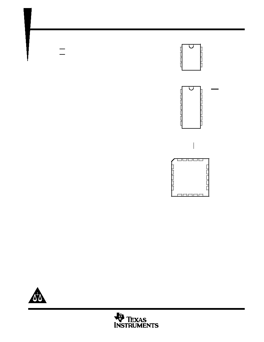
D, JG, OR P PACKAGE
1
2
3
4
5
6
7
14
13
12
11
10
9
8
C
XB
C
XA
NC
IN ≠
IN +
NC
V
DD ≠
INT/EXT
CLK IN
CLK OUT
V
DD +
OUT
CLAMP
C RETURN
D, J, OR N PACKAGE
(TOP VIEW)
NC ≠ No internal connection
3
2
1 20 19
9 10 11 12 13
4
5
6
7
8
18
17
16
15
14
CLK OUT
NC
V
DD +
NC
OUT
NC
NC
IN ≠
NC
IN +
FK PACKAGE
(TOP VIEW)
C
C
NC
C RETURN
CLAMP
INT/EXT
CLK IN
NC
V
NC
XA
XB
DD ≠
(TOP VIEW)
TLC2654, TLC2654A
Advanced LinCMOS
LOW-NOISE CHOPPER-STABILIZED
OPERATIONAL AMPLIFIERS
SLOS020G ≠ NOVEMBER 1988 ≠ REVISED APRIL 2001
2
POST OFFICE BOX 655303
∑
DALLAS, TEXAS 75265
description (continued)
The TLC2654 and TLC2654A common-mode
input voltage range includes the negative rail,
thereby providing superior performance in either
single-supply or split-supply applications, even at
power supply voltage levels as low as
±
2.3 V.
Two external capacitors are required to operate
the device; however, the on-chip chopper-control
circuitry is transparent to the user. On devices in
the 14-pin and 20-pin packages, the control
circuitry is accessible, allowing the user the option
of controlling the clock frequency with an external
frequency source. In addition, the clock threshold
of the TLC2554 and TLC2654A requires no level
shifting when used in the single-supply configura-
tion with a normal CMOS or TTL clock input.
Innovative circuit techniques used on the
TLC2654 and TLC2654A allow exceptionally fast
overload recovery time. An output clamp pin is
available to reduce the recovery time even further.
The device inputs and outputs are designed to
withstand ≠ 100-mA surge currents without
sustaining latch-up. In addition, the TLC2654 and TLC2654A incorporate internal ESD-protection circuits that
prevent functional failures at voltages up to 2000 V as tested under MIL-STD-883C, Method 3015; however,
exercise care in handling these devices, as exposure to ESD may result in degradation of the device parametric
performance.
The C-suffix devices are characterized for operation from 0
∞
C to 70
∞
C. The I-suffix devices are characterized
for operation from ≠ 40
∞
C to 85
∞
C. The Q-suffix devices are characterized for operation from ≠ 40
∞
C to 125
∞
C.
The M-suffix devices are characterized for operation over the full military temperature range of ≠ 55
∞
C to125
∞
C.
AVAILABLE OPTIONS
PACKAGED DEVICES
T
VIOmax
8 PIN
14 PIN
20 PIN
TA
VIOmax
AT 25
∞
C
SMALL
OUTLINE
(D)
CERAMIC
DIP
(JG)
PLASTIC
DIP
(P)
SMALL
OUTLINE
(D)
CERAMIC
DIP
(J)
PLASTIC
DIP
(N)
CERAMIC
DIP
(FK)
10
µ
V
TLC2654AC-8D
--
TLC2654ACP
TLC2654AC-14D
--
TLC2654ACN
--
0
∞
C to 70
∞
C
10
µ
V
20 mV
TLC2654AC-8D
TLC2654C 8D
--
TLC2654ACP
TLC2654CP
TLC2654AC-14D
TLC2654C 14D
--
TLC2654ACN
TLC2654CN
--
20 mV
TLC2654C-8D
--
TLC2654CP
TLC2654C-14D
--
TLC2654CN
--
10
µ
V
TLC2654AI-8D
--
TLC2654AIP
TLC2654AI-14D
--
TLC2654AIN
--
≠ 40
∞
C to 85
∞
C
10
µ
V
20
µ
V
TLC2654AI-8D
TLC2654I 8D
--
TLC2654AIP
TLC2654IP
TLC2654AI-14D
TLC2654I 14D
--
TLC2654AIN
TLC2654IN
--
20
µ
V
TLC2654I-8D
--
TLC2654IP
TLC2654I-14D
--
TLC2654IN
--
10
µ
V
TLC2654AQ-8D
--
--
--
--
--
--
≠ 40
∞
C to 125
∞
C
10
µ
V
20
µ
V
TLC2654AQ-8D
TLC2654Q 8D
--
--
--
--
--
--
20
µ
V
TLC2654Q-8D
--
--
--
--
--
--
10
µ
V
TLC2654AM-8D
TLC2654AMJG
TLC2654AMP
TLC2654AM-14D
TLC2654AMJ
TLC2654AMN
TLC2654AMFK
≠ 55
∞
C to 125
∞
C
10
µ
V
20
µ
V
TLC2654AM-8D
TLC2654M 8D
TLC2654AMJG
TLC2654MJG
TLC2654AMP
TLC2654MP
TLC2654AM-14D
TLC2654M 14D
TLC2654AMJ
TLC2654MJ
TLC2654AMN
TLC2654MN
TLC2654AMFK
TLC2654MFK
20
µ
V
TLC2654M-8D
TLC2654MJG
TLC2654MP
TLC2654M-14D
TLC2654MJ
TLC2654MN
TLC2654MFK
The 8-pin and 14-pin D packages are available taped and reeled. Add R suffix to device type (e.g., TLC2654AC-8DR).
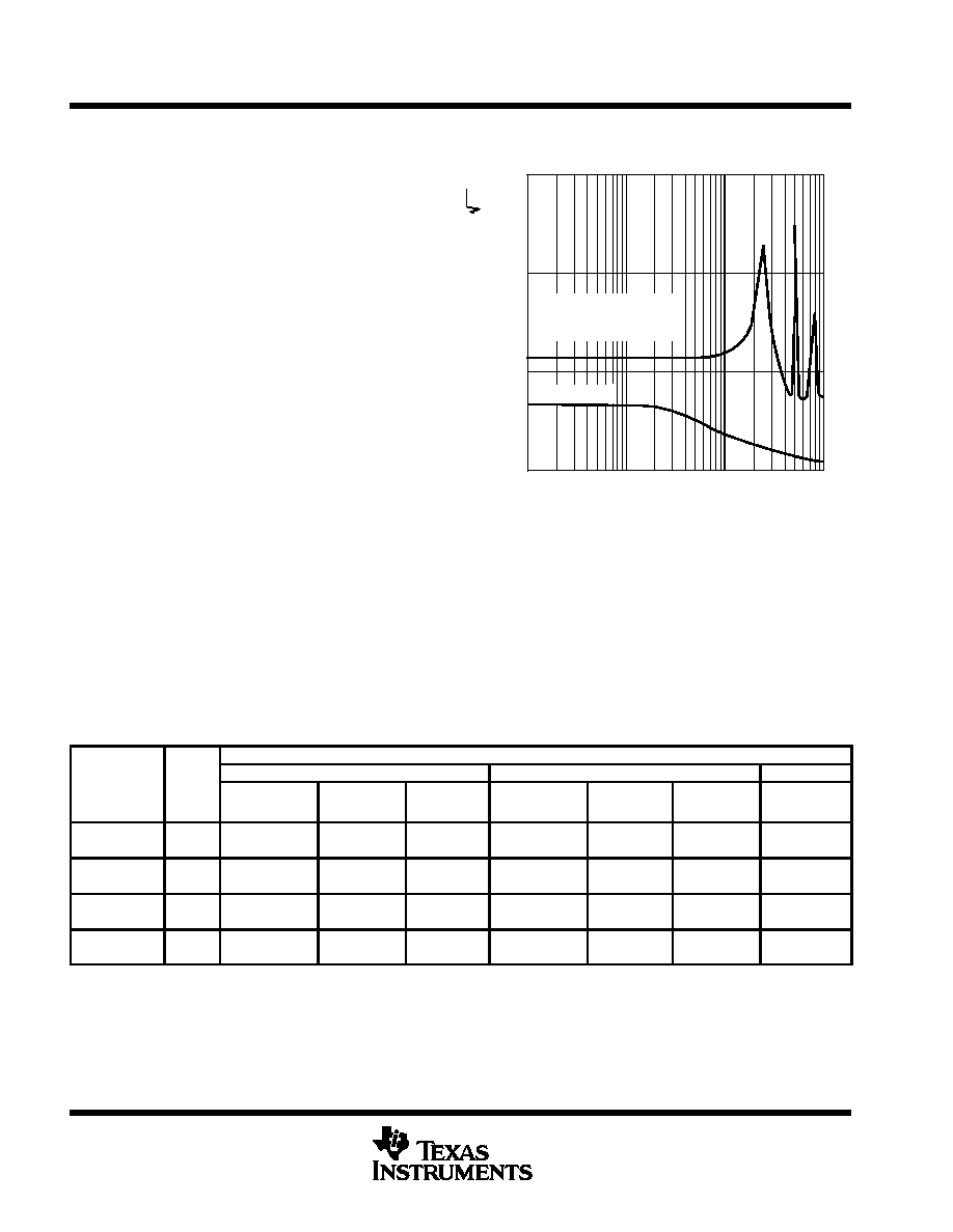
Vn
≠
Equivalent Input Noise V
oltage
≠
nV/XXVZ
EQUIVALENT INPUT NOISE VOLTAGE
vs
FREQUENCY
1 k
100
10
1
10
100
f ≠ Frequency ≠ Hz
1 k
10 k
V
n
nV/
Hz
Typical 250-Hz
Chopper-Stabilized
Operational Amplifier
TLC2654
Figure 1
TLC2654, TLC2654A
Advanced LinCMOS
LOW-NOISE CHOPPER-STABILIZED
OPERATIONAL AMPLIFIERS
SLOS020G ≠ NOVEMBER 1988 ≠ REVISED APRIL 2001
3
POST OFFICE BOX 655303
∑
DALLAS, TEXAS 75265
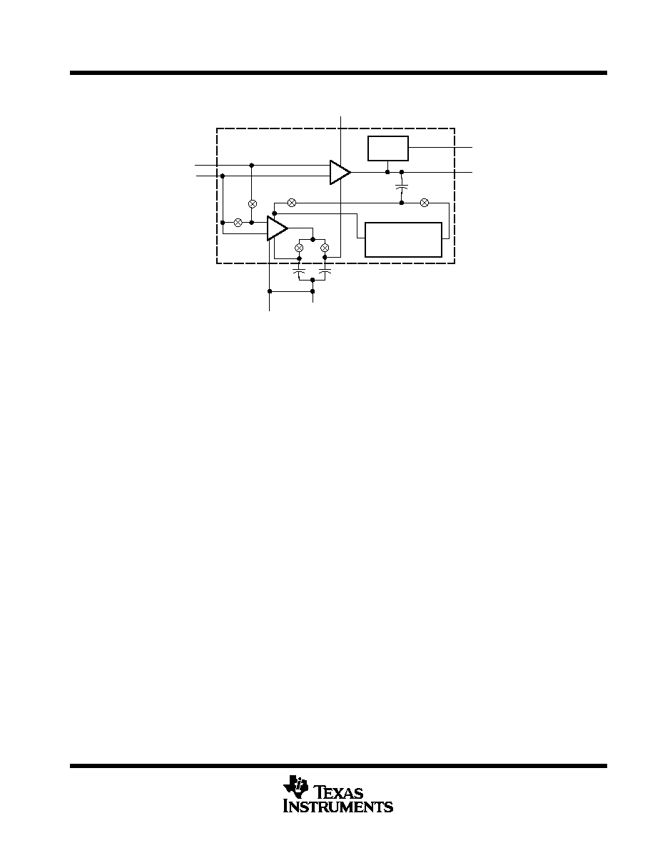
functional block diagram
External Components
C RETURN
VDD ≠
Null
IN +
IN ≠
VDD +
Main
CIC
CLAMP
OUT
CXB
CXA
Clamp
Circuit
Compensation-
Biasing
Circuit
A
A
A
B
B
B
5
4
11
1
2
7
8
9
10
+
≠
+
≠
Pin numbers shown are for the D (14 pin), J, and N packages.
TLC2654, TLC2654A
Advanced LinCMOS
LOW-NOISE CHOPPER-STABILIZED
OPERATIONAL AMPLIFIERS
SLOS020G ≠ NOVEMBER 1988 ≠ REVISED APRIL 2001
4
POST OFFICE BOX 655303
∑
DALLAS, TEXAS 75265
absolute maximum ratings over operating free-air temperature range (unless otherwise noted)
Supply voltage, V
DD +
(see Note 1)
8 V
. . . . . . . . . . . . . . . . . . . . . . . . . . . . . . . . . . . . . . . . . . . . . . . . . . . . . . . . . . . .
Supply voltage, V
DD ≠
(see Note 1)
≠ 8 V
. . . . . . . . . . . . . . . . . . . . . . . . . . . . . . . . . . . . . . . . . . . . . . . . . . . . . . . . . . .
Differential input voltage, V
ID
(see Note 2)
±
16 V
. . . . . . . . . . . . . . . . . . . . . . . . . . . . . . . . . . . . . . . . . . . . . . . . . . .
Input voltage, V
I
(any input, see Note 1)
±
8 V
. . . . . . . . . . . . . . . . . . . . . . . . . . . . . . . . . . . . . . . . . . . . . . . . . . . . . .
Voltage range on CLK IN and INT/EXT
V
DD ≠
to V
DD ≠
+ 5.2 V
. . . . . . . . . . . . . . . . . . . . . . . . . . . . . . . . . . . . . . .
Input current, I
I
(each input)
±
5
mA
. . . . . . . . . . . . . . . . . . . . . . . . . . . . . . . . . . . . . . . . . . . . . . . . . . . . . . . . . . . . . . .
Output current, I
O
±
50 mA
. . . . . . . . . . . . . . . . . . . . . . . . . . . . . . . . . . . . . . . . . . . . . . . . . . . . . . . . . . . . . . . . . . . . . . .
Duration of short-circuit current at (or below) 25
∞
C (see Note 3)
unlimited
. . . . . . . . . . . . . . . . . . . . . . . . . . . . . .
Current into CLK IN and INT/EXT
±
5
mA
. . . . . . . . . . . . . . . . . . . . . . . . . . . . . . . . . . . . . . . . . . . . . . . . . . . . . . . . . .
Continuous total dissipation
See Dissipation Rating Table
. . . . . . . . . . . . . . . . . . . . . . . . . . . . . . . . . . . . . . . . . . .
Operating free-air temperature range, T
A
: C suffix
0
∞
C to 70
∞
C
. . . . . . . . . . . . . . . . . . . . . . . . . . . . . . . . . . . . . .
I suffix
≠ 40
∞
C to 85
∞
C
. . . . . . . . . . . . . . . . . . . . . . . . . . . . . . . . . . . . .
Q suffix
≠ 40
∞
C to 125
∞
C
. . . . . . . . . . . . . . . . . . . . . . . . . . . . . . . . . . .
M suffix
≠ 55
∞
C to 125
∞
C
. . . . . . . . . . . . . . . . . . . . . . . . . . . . . . . . . . .
Storage temperature range
≠ 65
∞
C to 150
∞
C
. . . . . . . . . . . . . . . . . . . . . . . . . . . . . . . . . . . . . . . . . . . . . . . . . . . . . . . .
Case temperature for 60 seconds: FK package
260
∞
C
. . . . . . . . . . . . . . . . . . . . . . . . . . . . . . . . . . . . . . . . . . . . . .
Lead temperature 1,6 mm (1/16 inch) from case for 10 seconds: D, N, or P package
260
∞
C
. . . . . . . . . . . . .
Lead temperature 1,6 mm (1/16 inch) from case for 60 seconds: J or JG package
300
∞
C
. . . . . . . . . . . . . . . .
Stresses beyond those listed under "absolute maximum ratings" may cause permanent damage to the device. These are stress ratings only, and
functional operation of the device at these or any other conditions beyond those indicated under "recommended operating conditions" is not
implied. Exposure to absolute-maximum-rated conditions for extended periods may affect device reliability.
NOTES:
1. All voltage values, except differential voltages, are with respect to the midpoint between VDD + and VDD ≠ .
2. Differential voltages are at IN+ with respect to IN ≠.
3. The output may be shorted to either supply. Temperature and/or supply voltages must be limited to ensure that the maximum
dissipation rating is not exceeded.
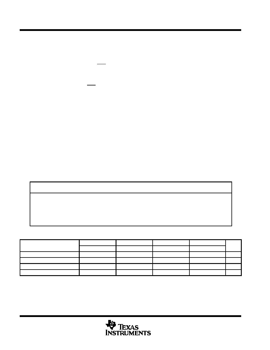
DISSIPATION RATING TABLE
PACKAGE
TA
25
∞
C
DERATING FACTOR
TA = 70
∞
C
TA = 85
∞
C
TA = 125
∞
C
PACKAGE
A
POWER RATING
ABOVE TA = 25
∞
C
A
POWER RATING
A
POWER RATING
A
POWER RATING
D (8 pin)
725 mW
5.8 mW/
∞
C
464 mW
377 mW
145 mW
D (8 in)
D (14 pin)
725 mW
950 mW
5.8 mW/ C
7.6 mW/
∞
C
464 mW
608 mW
377 mW
494 mW
145 mW
190 mW
(
)
FK
1375 mW
11.0 mW/
∞
C
880 mW
715 mW
275 mW
J
1375 mW
11.0 mW/
∞
C
880 mW
715 mW
275 mW
JG
1050 mW
8.4 mW/
∞
C
672 mW
546 mW
210 mW
N
1150 mW
9.2 mW/
∞
C
736 mW
598 mW
230 mW
P
1000 mW
8.0 mW/
∞
C
640 mW
520 mW
200 mW
recommended operating conditions
C SUFFIX
I SUFFIX
Q SUFFIX
M SUFFIX
UNIT
MIN
MAX
MIN
MAX
MIN
MAX
MIN
MAX
UNIT
Supply voltage, VDD
±
±
2.3
±
8
±
2.3
±
8
±
2.3
±
8
±
2.3
±
8
V
Common-mode input voltage, VIC
VDD ≠ VDD + ≠ 2.3
VDD ≠ VDD + ≠ 2.3
VDD ≠ VDD + ≠ 2.3 VDD ≠ VDD + ≠ 2.3
V
Clock input voltage
VDD ≠
VDD ≠ + 5
VDD ≠
VDD ≠ + 5
VDD ≠
VDD ≠ + 5 VDD ≠
VDD ≠ + 5
V
Operating free-air temperature, TA
0
70
≠ 40
85
≠ 40
125
≠ 55
125
∞
C

TLC2654, TLC2654A
Advanced LinCMOS
LOW-NOISE CHOPPER-STABILIZED
OPERATIONAL AMPLIFIERS
SLOS020G ≠ NOVEMBER 1988 ≠ REVISED APRIL 2001
5
POST OFFICE BOX 655303
∑
DALLAS, TEXAS 75265
electrical characteristics at specified free-air temperature, V
DD
±
=
±
5 V (unless otherwise noted)
PARAMETER
TEST CONDITIONS
TA
TLC2654C
TLC2654AC
UNIT
PARAMETER
TEST CONDITIONS
TA
MIN
TYP
MAX
MIN
TYP
MAX
UNIT
VIO
Input offset voltage
25
∞
C
5
20
4
10
µ
V
VIO
g
(see Note 4)
Full range
34
24
µ
V
VIO
Temperature coefficient of
Full range
0 01
0 05
0 01
0 05
µ
V/
∞
C
VIO
input offset voltage
Full range
0.01
0.05
0.01
0.05
µ
V/
∞
C
Input offset voltage
long-term drift (see Note 5)
VIC = 0,
RS = 50
25
∞
C
0.003
0.06
0.003
0.02
µ
V/mo
IIO
Input offset current
25
∞
C
30
60
30
60
pA
IIO
Input offset current
Full range
150
150
pA
IIB
Input bias current
25
∞
C
50
60
50
60
pA
IIB
Input bias current
Full range
150
150
pA
VICR
Common-mode input
RS = 50
Full range
≠ 5
to
≠ 5
to
V
VICR
voltage range
RS = 50
Full range
to
2.7
to
2.7
V
VOM
Maximum positive peak
RL = 10 k
See Note 6
25
∞
C
4.7
4.8
4.7
4.8
V
VOM +
output voltage swing
RL = 10 k
,
See Note 6
Full range
4.7
4.7
V
VOM
Maximum negative peak
RL = 10 k
See Note 6
25
∞
C
≠ 4.7
≠ 4.9
≠ 4.7
≠ 4.9
V
VOM ≠
g
output voltage swing
RL = 10 k
,
See Note 6
Full range
≠ 4.7
≠ 4.7
V
AVD
Large-signal differential
VO =
±
4 V
RL = 10 k
25
∞
C
120
155
135
155
dB
AVD
g
g
voltage amplification
VO =
±
4 V,
RL = 10 k
Full range
120
130
dB
Internal chopping
frequency
25
∞
C
10
10
kHz
Clamp on state current
RL = 100 k
25
∞
C
25
25
µ
A
Clamp on-state current
RL = 100 k
Full range
25
25
µ
A
Clamp off state current
VO =
4 V to 4 V
25
∞
C
100
100
pA
Clamp off-state current
VO = ≠ 4 V to 4 V
Full range
100
100
pA
CMRR
Common-mode rejection
VO = 0,
VIC VICRmin
25
∞
C
105
125
110
125
dB
CMRR
j
ratio
VIC = VICRmin,
RS = 50
Full range
105
110
dB
kSVR
Supply voltage rejection
VDD
±
=
±
2.3 V to
±
8 V,
25
∞
C
110
125
110
125
dB
kSVR
y
g
j
ratio (
VDD
±
/
VIO)
DD
±
,
VO = 0,
RS = 50
Full range
110
110
dB
IDD
Supply current
VO = 0
No load
25
∞
C
1.5
2.4
1.5
2.4
mA
IDD
Supply current
VO = 0,
No load
Full range
2.5
2.5
mA
Full range is 0
∞
C to 70
∞
C.
NOTES:
4. This parameter is not production tested full range. Thermocouple effects preclude measurement of the actual VIO of these devices
in high-speed automated testing. VIO is measured to a limit determined by the test equipment capability at the temperature extremes.
The test ensures that the stabilization circuitry is performing properly.
5. Typical values are based on the input offset voltage shift observed through 168 hours of operating life test at TA = 150
∞
C extrapolated
to TA = 25
∞
using the Arrhenius equation and assuming an activation energy of 0.96 eV.
6. Output clamp is not connected.