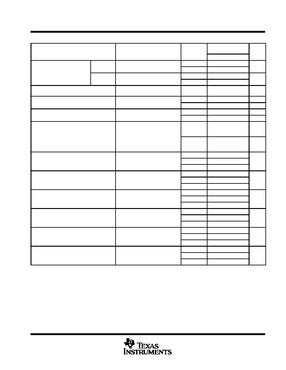
TLC27L4, TLC27L4A, TLC27L4B, TLC27L4Y, TLC27L9
LinCMOS
TM
PRECISION QUAD OPERATIONAL AMPLIFIERS
SLOS053C ≠ OCTOBER 1987 ≠ REVISED AUGUST 1994
1
POST OFFICE BOX 655303
∑
DALLAS, TEXAS 75265
D
Trimmed Offset Voltage:
TLC27L9 . . . 900
µ
V Max at 25
∞
C,
V
DD
= 5 V
D
Input Offset Voltage Drift . . . Typically
0.1
µ
V/Month, Including the First 30 Days
D
Wide Range of Supply Voltages Over
Specified Temperature Range:
0
∞
C to 70
∞
C . . . 3 V to 16 V
≠ 40
∞
C to 85
∞
C . . . 4 V to 16 V
≠ 55
∞
C to 125
∞
C . . . 4 V to 16 V
D
Single-Supply Operation
D
Common-Mode Input Voltage Range
Extends Below the Negative Rail (C-Suffix,
I-Suffix Types)
D
Ultra-Low Power . . . Typically 195
µ
W
at 25
∞
C, V
DD
= 5 V
D
Output Voltage Range includes Negative
Rail
D
High Input Impedance . . . 10
12
Typ
D
ESD-Protection Circuitry
D
Small-Outline Package Option Also
Available in Tape and Reel
D
Designed-In Latch-Up Immunity
description
The TLC27L4 and TLC27L9 quad operational
amplifiers combine a wide range of input offset
voltage grades with low offset voltage drift, high
input impedance, extremely low power, and high
gain.
These devices use Texas instruments silicon-gate
LinCMOS
TM
technology, which provides offset
voltage stability far exceeding the stability
available with conventional metal-gate pro-
cesses.
The extremely high input impedance, low bias
currents, and low-power consumption make
these cost-effective devices ideal for high-gain,
low- frequency, low-power applications. Four
offset voltage grades are available (C-suffix and
I-suffix types), ranging from the low-cost TLC27L4
(10 mV) to the high-precision TLC27L9 (900
µ
V).
These advantages, in combination with good
common-mode rejection and supply voltage
rejection, make these devices a good choice for
new state-of-the-art designs as well as for
upgrading existing designs.
Copyright
©
1994, Texas Instruments Incorporated
PRODUCTION DATA information is current as of publication date.
Products conform to specifications per the terms of Texas Instruments
standard warranty. Production processing does not necessarily include
testing of all parameters.
LinCMOS is a trademark of Texas Instruments Incorporated.
35
30
25
20
15
10
5
600
0
≠ 600
40
1200
VIO ≠ Input Offset Voltage ≠
µ
V
Percentage of Units ≠ %
0
≠ 1200
N Package
TA = 25
∞
C
VDD = 5 V
299 Units Tested From 2 Wafer Lots
DISTRIBUTION OF TLC27L9
INPUT OFFSET VOLTAGE
1
2
3
4
5
6
7
14
13
12
11
10
9
8
1OUT
1IN ≠
1IN +
V
DD
2IN +
2IN ≠
2OUT
4OUT
4IN ≠
4IN +
GND
3IN +
3IN ≠
3OUT
D, J, N, OR PW PACKAGE
(TOP VIEW)
3
2
1 20 19
9 10 11 12 13
4
5
6
7
8
18
17
16
15
14
4IN +
NC
GND
NC
3IN +
1IN +
NC
V
DD
NC
2IN +
FK PACKAGE
(TOP VIEW)
1IN ≠
1OUT
NC
3OUT
3IN ≠
4OUT
4IN ≠
2IN ≠
2OUT
NC
NC ≠ No internal connection
TLC27L4, TLC27L4A, TLC27L4B, TLC27L4Y, TLC27L9
LinCMOS
TM
PRECISION QUAD OPERATIONAL AMPLIFIERS
SLOS053C ≠ OCTOBER 1987 ≠ REVISED AUGUST 1994
2
POST OFFICE BOX 655303
∑
DALLAS, TEXAS 75265
description (continued)
In general, many features associated with bipolar technology are available on LinCMOS
TM
operational
amplifiers, without the power penalties of bipolar technology. General applications such as transducer
interfacing, analog calculations, amplifier blocks, active filters, and signal buffering are easily designed with the
TLC27L4 and TLC27L9. The devices also exhibit low voltage single-supply operation and ultra-low power
consumption, making them ideally suited for remote and inaccessible battery-powered applications. The
common-mode input voltage range includes the negative rail.
A wide range of packaging options is available, including small-outline and chip-carrier versions for high-density
system applications.
The device inputs and outputs are designed to withstand ≠100-mA surge currents without sustaining latch-up.
The TLC27L4 and TLC27L9 incorporate internal ESD-protection circuits that prevent functional failures at
voltages up to 2000 V as tested under MIL-STD-883C, Method 3015.2; however, care should be exercised in
handling these devices, as exposure to ESD may result in the degradation of the device parametric
performance.
The C-suffix devices are characterized for operation from 0
∞
C to 70
∞
C. The I-suffix devices are characterized
for operation from ≠ 40
∞
C to 85
∞
C. The M-suffix devices are characterized for operation from ≠ 55
∞
C to 125
∞
C.
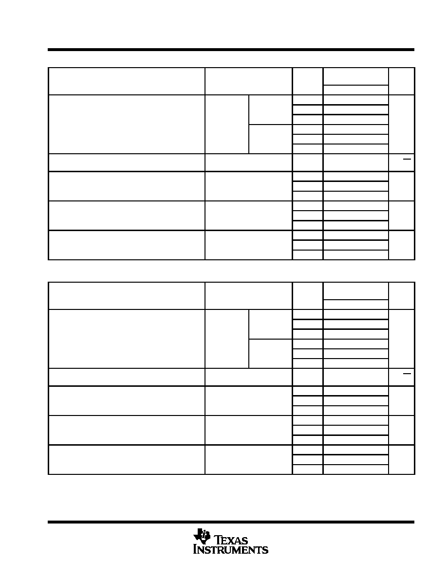
AVAILABLE OPTIONS
PACKAGED DEVICES
CHIP
TA
VIOmax
AT 25
∞
C
SMALL
OUTLINE
(D)
CHIP
CARRIER
(FK)
CERAMIC
DIP
(J)
PLASTIC
DIP
(N)
TSSOP
(PW)
CHIP
FORM
(Y)
900
µ
V
TLC27L9CD
--
--
TLC27L9CN
--
--
0
∞
C to 70
∞
C
2 mV
TLC27L4BCD
--
--
TLC27L4BCN
--
--
0
∞
C to 70
∞
C
5 mV
TLC27L4ACD
--
--
TLC27L4ACN
--
--
10 mV
TLC27L4CD
--
--
TLC27L4CN
TLC27L4CPW
TLC27L4Y
900
µ
V
TLC27L9ID
--
--
TLC27L9IN
--
--
40
∞
C to 85
∞
C
2 mV
TLC27L4BID
--
--
TLC27L4BIN
--
--
≠ 40
∞
C to 85
∞
C
5 mV
TLC27L4AID
--
--
TLC27L4AIN
--
--
10 mV
TLC27L4ID
--
--
TLC27L4IN
--
--
55
∞
C to 125
∞
C
900
µ
V
TLC27L9MD
TLC27L9MFK
TLC27L9MJ
TLC27L9MN
--
--
≠ 55
∞
C to 125
∞
C
10 mV
TLC27L4MD
TLC27L4MFK
TLC27L4MJ
TLC27L4MN
--
--
The D package is available taped and reeled. Add R suffix to the device type (e.g., TLC27L9CDR).
TLC27L4, TLC27L4A, TLC27L4B, TLC27L4Y, TLC27L9
LinCMOS
TM
PRECISION QUAD OPERATIONAL AMPLIFIERS
SLOS053C ≠ OCTOBER 1987 ≠ REVISED AUGUST 1994
3
POST OFFICE BOX 655303
∑
DALLAS, TEXAS 75265
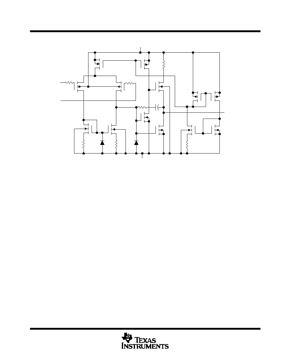
equivalent schematic (each amplifier)
VDD
P4
P3
R6
N5
R2
P2
R1
P1
IN ≠
IN +
N1
R3
D1
R4
D2
N2
GND
N3
R5
C1
N4
R7
N6
N7
OUT
P6
P5
TLC27L4, TLC27L4A, TLC27L4B, TLC27L4Y, TLC27L9
LinCMOS
TM
PRECISION QUAD OPERATIONAL AMPLIFIERS
SLOS053C ≠ OCTOBER 1987 ≠ REVISED AUGUST 1994
4
POST OFFICE BOX 655303
∑
DALLAS, TEXAS 75265
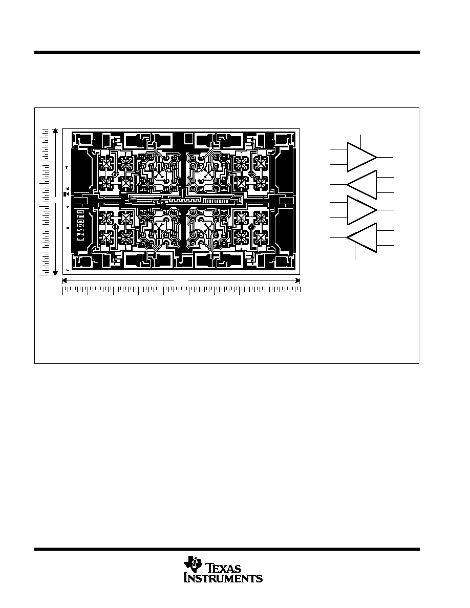
TLC27L4Y chip information
These chips, when properly assembled, display characteristics similar to the TLC27L4C. Thermal compression
or ultrasonic bonding may be used on the doped-aluminum bonding pads. Chips may be mounted with
conductive epoxy or a gold-silicon preform.
BONDING PAD ASSIGNMENTS
CHIP THICKNESS: 15 TYPICAL
BONDING PADS: 4
◊
4 MINIMUM
TJmax = 150
∞
C
TOLERANCES ARE
±
10%.
ALL DIMENSIONS ARE IN MILS.
PIN (11) IS INTERNALLY CONNECTED
TO BACKSIDE OF CHIP.
+
≠
1OUT
1IN +
1IN ≠
VDD
(4)
(6)
(3)
(2)
(5)
(1)
≠
+
(7)
2IN +
2IN ≠
2OUT
(11)
GND
+
≠
3OUT
3IN +
3IN ≠
(13)
(10)
(9)
(12)
(8)
≠
+
(14)
4OUT
4IN +
4IN ≠
68
108
(1)
(2)
(3)
(4)
(5)
(6)
(7)
(8)
(9)
(10)
(11)
(12)
(13)
(14)
TLC27L4, TLC27L4A, TLC27L4B, TLC27L4Y, TLC27L9
LinCMOS
TM
PRECISION QUAD OPERATIONAL AMPLIFIERS
SLOS053C ≠ OCTOBER 1987 ≠ REVISED AUGUST 1994
5
POST OFFICE BOX 655303
∑
DALLAS, TEXAS 75265
absolute maximum ratings over operating free-air temperature (unless otherwise noted)
Supply voltage, V
DD
(see Note 1)
18 V
. . . . . . . . . . . . . . . . . . . . . . . . . . . . . . . . . . . . . . . . . . . . . . . . . . . . . . . . . . . .
Differential input voltage, V
ID
(see Note 2)
±
V
DD
. . . . . . . . . . . . . . . . . . . . . . . . . . . . . . . . . . . . . . . . . . . . . . . . . . .
Input voltage range, V
I
(any input)
≠ 0.3 V to V
DD
. . . . . . . . . . . . . . . . . . . . . . . . . . . . . . . . . . . . . . . . . . . . . . . . . . .
Input current, I
I
±
5 mA
. . . . . . . . . . . . . . . . . . . . . . . . . . . . . . . . . . . . . . . . . . . . . . . . . . . . . . . . . . . . . . . . . . . . . . . . . .
Output current, I
O
(each output)
±
30 mA
. . . . . . . . . . . . . . . . . . . . . . . . . . . . . . . . . . . . . . . . . . . . . . . . . . . . . . . . . .
Total current into V
DD
45 mA
. . . . . . . . . . . . . . . . . . . . . . . . . . . . . . . . . . . . . . . . . . . . . . . . . . . . . . . . . . . . . . . . . . . .
Total current out of GND
45 mA
. . . . . . . . . . . . . . . . . . . . . . . . . . . . . . . . . . . . . . . . . . . . . . . . . . . . . . . . . . . . . . . . . .
Duration of short-circuit current at (or below) 25
∞
C (see Note 3)
unlimited
. . . . . . . . . . . . . . . . . . . . . . . . . . . . . .
Continuous total dissipation
See Dissipation Rating Table
. . . . . . . . . . . . . . . . . . . . . . . . . . . . . . . . . . . . . . . . . . .
Operating free-air temperature, T
A
: C suffix
0
∞
C to 70
∞
C
. . . . . . . . . . . . . . . . . . . . . . . . . . . . . . . . . . . . . . . . . . . .
I suffix
≠ 40
∞
C to 85
∞
C
. . . . . . . . . . . . . . . . . . . . . . . . . . . . . . . . . . . . . . . . . . .
M suffix
≠ 55
∞
C to 125
∞
C
. . . . . . . . . . . . . . . . . . . . . . . . . . . . . . . . . . . . . . . .
Storage temperature range
≠ 65
∞
C to 150
∞
C
. . . . . . . . . . . . . . . . . . . . . . . . . . . . . . . . . . . . . . . . . . . . . . . . . . . . . . . .
Case temperature for 60 seconds: FK package
260
∞
C
. . . . . . . . . . . . . . . . . . . . . . . . . . . . . . . . . . . . . . . . . . . . . .
Lead temperature 1,6 mm (1/16 inch) from case for 10 seconds: D, N, or PW package
260
∞
C
. . . . . . . . . . . .
Lead temperature 1,6 mm (1/16 inch) from case for 60 seconds: J package
300
∞
C
. . . . . . . . . . . . . . . . . . . . .
Stresses beyond those listed under "absolute maximum ratings" may cause permanent damage to the device. These are stress ratings only, and
functional operation of the device at these or any other conditions beyond those indicated under "recommended operating conditions" is not
implied. Exposure to absolute-maximum-rated conditions for extended periods may affect device reliability.
NOTES:
1. All voltage values, except differential voltages, are with respect to network ground.
2. Differential voltages are at IN+ with respect to IN ≠.
3. The output may be shorted to either supply. Temperature and /or supply voltages must be limited to ensure that the maximum
dissipation rating is not exceeded (see application section).
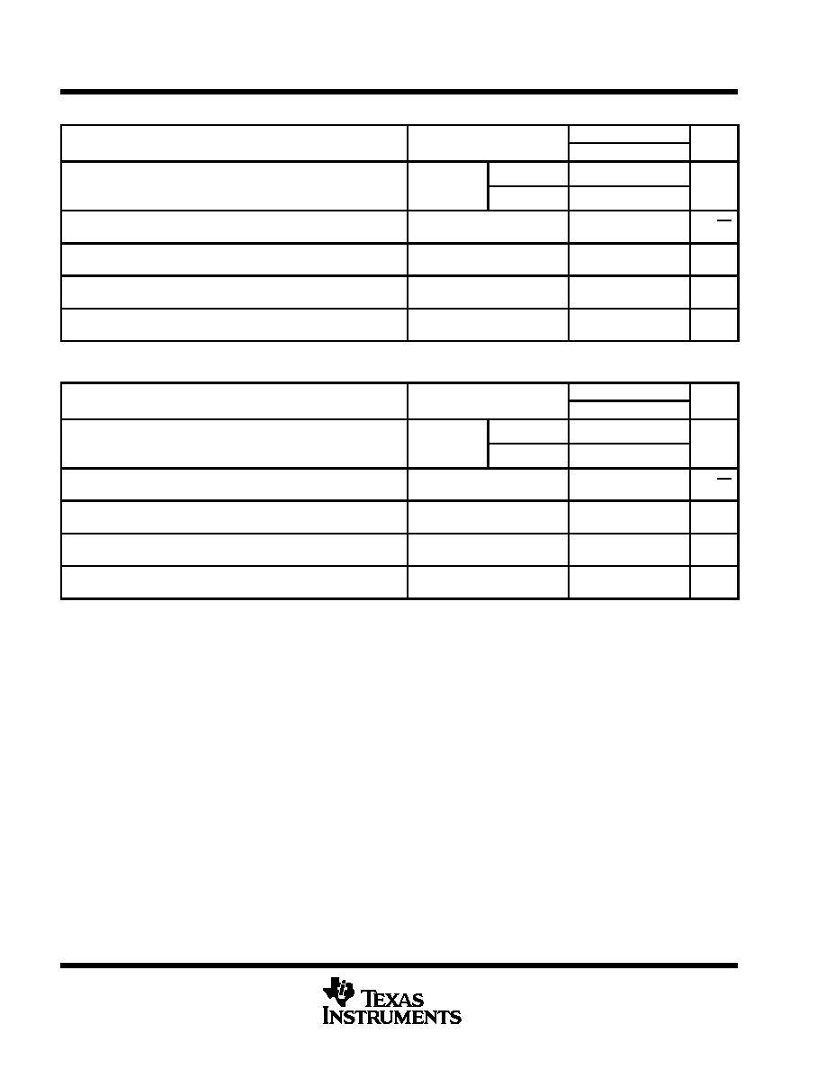
DISSIPATION RATING TABLE
PACKAGE
TA
25
∞
C
POWER RATING
DERATING FACTOR
ABOVE TA = 25
∞
C
TA = 70
∞
C
POWER RATING
TA = 85
∞
C
POWER RATING
TA = 125
∞
C
POWER RATING
D
950 mW
7.6 mW/
∞
C
608 mW
494 mW
--
FK
1375 mW
11.0 mW/
∞
C
880 mW
715 mW
275 mW
J
1375 mW
11.0 mW/
∞
C
880 mW
715 mW
275 mW
N
1575 mW
12.6 mW/
∞
C
1008 mW
819 mW
--
PW
700 mW
5.6 mW/
∞
C
448 mW
--
--
recommended operating conditions
C SUFFIX
I SUFFIX
M SUFFIX
UNIT
MIN
MAX
MIN
MAX
MIN
MAX
UNIT
Supply voltage, VDD
3
16
4
16
4
16
V
Common mode input voltage VIC
VDD = 5 V
≠ 0.2
3.5
≠ 0.2
3.5
0
3.5
V
Common-mode input voltage, VIC
VDD = 10 V
≠ 0.2
8.5
≠ 0.2
8.5
0
8.5
V
Operating free-air temperature, TA
0
70
≠ 40
85
≠ 55
125
∞
C
TLC27L4, TLC27L4A, TLC27L4B, TLC27L4Y, TLC27L9
LinCMOS
TM
PRECISION QUAD OPERATIONAL AMPLIFIERS
SLOS053C ≠ OCTOBER 1987 ≠ REVISED AUGUST 1994
6
POST OFFICE BOX 655303
∑
DALLAS, TEXAS 75265
electrical characteristics at specified free-air temperature, V
DD
= 5 V (unless otherwise noted)
PARAMETER
TEST CONDITIONS
TA
TLC27L4C
TLC27L4AC
TLC27L4BC
TLC27L9C
UNIT
MIN
TYP
MAX
TLC27L4C
VO = 1.4 V,
VIC = 0,
25
∞
C
1.1
10
TLC27L4C
O
,
RS = 50
,
IC
,
RL = 1 M
Full range
12
mV
TLC27L4AC
VO = 1.4 V,
VIC = 0,
25
∞
C
0.9
5
mV
VIO
Input offset voltage
TLC27L4AC
O
,
RS = 50
,
IC
,
RL = 1 M
Full range
6.5
VIO
Input offset voltage
TLC27L4BC
VO = 1.4 V,
VIC = 0,
25
∞
C
240
2000
TLC27L4BC
O
,
RS = 50
,
IC
,
RL = 1 M
Full range
3000
µ
V
TLC27L9C
VO = 1.4 V,
VIC = 0,
25
∞
C
200
900
µ
V
TLC27L9C
O
,
RS = 50
,
IC
,
RL = 1 M
Full range
1500
VIO
Average temperature coefficient of input
offset voltage
25
∞
C to
70
∞
C
1.1
µ
V/
∞
C
IIO
Input offset current (see Note 4)
VO = 2 5 V
VIC = 2 5 V
25
∞
C
0.1
pA
IIO
Input offset current (see Note 4)
VO = 2.5 V,
VIC = 2.5 V
70
∞
C
7
300
pA
IIB
Input bias current (see Note 4)
VO = 2 5 V
VIC = 2 5 V
25
∞
C
0.6
pA
IIB
Input bias current (see Note 4)
VO = 2.5 V,
VIC = 2.5 V
70
∞
C
40
600
pA
VICR
Common mode input voltage range
25
∞
C
≠ 0.2
to
4
≠ 0.3
to
4.2
V
VICR
g
g
(see Note 5)
Full range
≠ 0.2
to
3.5
V
25
∞
C
3.2
4.1
VOH
High-level output voltage
VID = 100 mV,
RL = 1 M
0
∞
C
3
4.1
V
70
∞
C
3
4.2
25
∞
C
0
50
VOL
Low-level output voltage
VID = ≠100 mV,
IOL = 0
0
∞
C
0
50
mV
70
∞
C
0
50
L
i
l diff
ti l
lt
25
∞
C
50
520
AVD
Large-signal differential voltage
amplification
VO = 2.5 V to 2 V,
RL = 1 M
0
∞
C
50
680
V/mV
am lification
70
∞
C
50
380
25
∞
C
65
94
CMRR
Common-mode rejection ratio
VIC = VICRmin
0
∞
C
60
95
dB
70
∞
C
60
95
S
l
lt
j
ti
ti
25
∞
C
70
97
kSVR
Supply-voltage rejection ratio
(
VDD /
VIO)
VDD = 5 V to 10 V, VO = 1.4 V
0
∞
C
60
97
dB
(
VDD /
VIO)
70
∞
C
60
98
V
2 5 V
V
2 5 V
25
∞
C
40
68
IDD
Supply current (four amplifiers)
VO = 2.5 V,
No load
VIC = 2.5 V,
0
∞
C
48
84
µ
A
No load
70
∞
C
31
56
Full range is 0
∞
C to 70
∞
C.
NOTES:
4. The typical values of input bias current and input offset current below 5 pA were determined mathematically.
5. This range also applies to each input individually.
TLC27L4, TLC27L4A, TLC27L4B, TLC27L4Y, TLC27L9
LinCMOS
TM
PRECISION QUAD OPERATIONAL AMPLIFIERS
SLOS053C ≠ OCTOBER 1987 ≠ REVISED AUGUST 1994
7
POST OFFICE BOX 655303
∑
DALLAS, TEXAS 75265
electrical characteristics at specified free-air temperature, V
DD
= 10 V (unless otherwise noted)
PARAMETER
TEST CONDITIONS
TA
TLC27L4C
TLC27L4AC
TLC27L4BC
TLC27L9C
UNIT
MIN
TYP
MAX
TLC27L4C
VO = 1.4 V,
VIC = 0,
25
∞
C
1.1
10
TLC27L4C
O
,
RS = 50
,
IC
,
RL = 1 M
Full range
12
mV
TLC27L4AC
VO = 1.4 V,
VIC = 0,
25
∞
C
0.9
5
mV
VIO
Input offset voltage
TLC27L4AC
O
,
RS = 50
,
IC
,
RL = 1 M
Full range
6.5
VIO
Input offset voltage
TLC27L4BC
VO = 1.4 V,
VIC = 0,
25
∞
C
260
2000
TLC27L4BC
O
,
RS = 50
,
IC
,
RL = 1 M
Full range
3000
µ
V
TLC27L9C
VO = 1.4 V,
VIC = 0,
25
∞
C
210
1200
µ
V
TLC27L9C
O
,
RS = 50
,
IC
,
RL = 1 M
Full range
1900
VIO
Average temperature coefficient of
input offset voltage
25
∞
C to
70
∞
C
1
µ
V/
∞
C
IIO
Input offset current (see Note 4)
VO = 5 V
VIC = 5 V
25
∞
C
0.1
pA
IIO
Input offset current (see Note 4)
VO = 5 V,
VIC = 5 V
70
∞
C
7
300
pA
IIB
Input bias current (see Note 4)
VO = 5 V
VIC = 5 V
25
∞
C
0.7
pA
IIB
Input bias current (see Note 4)
VO = 5 V,
VIC = 5 V
70
∞
C
50
600
pA
VICR
Common-mode input voltage range
25
∞
C
≠ 0.2
to
9
≠ 0.3
to
9.2
V
VICR
g
g
(see Note 5)
Full range
≠ 0.2
to
8.5
V
25
∞
C
8
8.9
VOH
High-level output voltage
VID = 100 mV,
RL = 1 M
0
∞
C
7.8
8.9
V
70
∞
C
7.8
8.9
25
∞
C
0
50
VOL
Low-level output voltage
VID = ≠100 mV,
IOL = 0
0
∞
C
0
50
mV
70
∞
C
0
50
L
i
l diff
ti l
lt
25
∞
C
50
870
AVD
Large-signal differential voltage
amplification
VO = 1 V to 6 V,
RL = 1 M
0
∞
C
50
1020
V/mV
am lification
70
∞
C
50
660
25
∞
C
65
97
CMRR
Common-mode rejection ratio
VIC = VICRmin
0
∞
C
60
97
dB
70
∞
C
60
97
S
l
lt
j
ti
ti
25
∞
C
70
97
kSVR
Supply-voltage rejection ratio
(
VDD /
VIO)
VDD = 5 V to 10 V, VO = 1.4 V
0
∞
C
60
97
dB
(
VDD /
VIO)
70
∞
C
60
98
V
5 V
V
5 V
25
∞
C
57
92
IDD
Supply current (four amplifiers)
VO = 5 V,
No load
VIC = 5 V,
0
∞
C
72
132
µ
A
No load
70
∞
C
44
80
Full range is 0
∞
C to 70
∞
C.
NOTES:
4. The typical values of input bias current and input offset current below 5 pA were determined mathematically.
5. This range also applies to each input individually.

TLC27L4, TLC27L4A, TLC27L4B, TLC27L4Y, TLC27L9
LinCMOS
TM
PRECISION QUAD OPERATIONAL AMPLIFIERS
SLOS053C ≠ OCTOBER 1987 ≠ REVISED AUGUST 1994
8
POST OFFICE BOX 655303
∑
DALLAS, TEXAS 75265
electrical characteristics at specified free-air temperature, V
DD
=
5 V (unless otherwise noted)
PARAMETER
TEST CONDITIONS
TA
TLC27L4I
TLC27L4AI
TLC27L4BI
TLC27L9I
UNIT
MIN
TYP
MAX
TLC27L4I
VO = 1.4 V,
VIC = 0,
25
∞
C
1.1
10
TLC27L4I
O
,
RS = 50
,
IC
,
RL = 1 M
Full range
13
mV
TLC27L4AI
VO = 1.4 V,
VIC = 0,
25
∞
C
0.9
5
mV
VIO
Input offset voltage
TLC27L4AI
O
,
RS = 50
,
IC
,
RL = 1 M
Full range
7
VIO
Input offset voltage
TLC27L4BI
VO = 1.4 V,
VIC = 0,
25
∞
C
240
2000
TLC27L4BI
O
,
RS = 50
,
IC
,
RL = 1 M
Full range
3500
µ
V
TLC27L9I
VO = 1.4 V,
VIC = 0,
25
∞
C
200
900
µ
V
TLC27L9I
O
,
RS = 50
,
IC
,
RL = 1 M
Full range
2000
VIO
Average temperature coefficient of input
offset voltage
25
∞
C to
85
∞
C
1.1
µ
V/
∞
C
IIO
Input offset current (see Note 4)
VO = 2 5 V
VIC = 2 5 V
25
∞
C
0.1
pA
IIO
Input offset current (see Note 4)
VO = 2.5 V,
VIC = 2.5 V
85
∞
C
24
1000
pA
IIB
Input bias current (see Note 4)
VO = 2 5 V
VIC = 2 5 V
25
∞
C
0.6
pA
IIB
Input bias current (see Note 4)
VO = 2.5 V,
VIC = 2.5 V
85
∞
C
200
2000
pA
VICR
Common-mode input voltage range
25
∞
C
≠ 0.2
to
4
≠ 0.3
to
4.2
V
VICR
g
g
(see Note 5)
Full range
≠ 0.2
to
3.5
V
25
∞
C
3.2
4.1
VOH
High-level output voltage
VID = 100 mV,
RL = 1 M
≠ 40
∞
C
3
4.1
V
85
∞
C
3
4.2
25
∞
C
0
50
VOL
Low-level output voltage
VID = ≠100 mV,
IOL = 0
≠ 40
∞
C
0
50
mV
85
∞
C
0
50
L
i
l diff
ti l
lt
25
∞
C
50
480
AVD
Large-signal differential voltage
amplification
VO = 0.25 V to 2 V,
RL = 1 M
≠ 40
∞
C
50
900
V/mV
am lification
85
∞
C
50
330
25
∞
C
65
94
CMRR
Common-mode rejection ratio
VIC = VICRmin
≠ 40
∞
C
60
95
dB
85
∞
C
60
95
S
l
lt
j
ti
ti
25
∞
C
70
97
kSVR
Supply-voltage rejection ratio
(
VDD /
VIO)
VDD = 5 V to 10 V,
VO = 1.4 V
≠ 40
∞
C
60
97
dB
(
VDD /
VIO)
85
∞
C
60
98
V
2 5 V
V
2 5 V
25
∞
C
39
68
IDD
Supply current (four amplifiers)
VO = 2.5 V,
No load
VIC = 2.5 V,
≠ 40
∞
C
62
108
µ
A
No load
85
∞
C
29
52
Full range is ≠ 40
∞
C to 85
∞
C.
NOTES:
4. The typical values of input bias current and input offset current below 5 pA were determined mathematically.
5. This range also applies to each input individually.

TLC27L4, TLC27L4A, TLC27L4B, TLC27L4Y, TLC27L9
LinCMOS
TM
PRECISION QUAD OPERATIONAL AMPLIFIERS
SLOS053C ≠ OCTOBER 1987 ≠ REVISED AUGUST 1994
9
POST OFFICE BOX 655303
∑
DALLAS, TEXAS 75265
electrical characteristics at specified free-air temperature, V
DD
= 10 V (unless otherwise noted)
PARAMETER
TEST CONDITIONS
TA
TLC27L4I
TLC27L4AI
TLC27L4BI
TLC27L9I
UNIT
MIN
TYP
MAX
TLC27L4I
VO = 1.4 V,
VIC = 0,
25
∞
C
1.1
10
TLC27L4I
O
,
RS = 50
,
IC
,
RL = 1 M
Full range
13
mV
TLC27L4AI
VO = 1.4 V,
VIC = 0,
25
∞
C
0.9
5
mV
VIO
Input offset voltage
TLC27L4AI
O
,
RS = 50
,
IC
,
RL = 1 M
Full range
7
VIO
Input offset voltage
TLC27L4BI
VO = 1.4 V,
VIC = 0,
25
∞
C
260
2000
TLC27L4BI
O
,
RS = 50
,
IC
,
RL = 1 M
Full range
3500
µ
V
TLC27L9I
VO = 1.4 V,
VIC = 0,
25
∞
C
210
1200
µ
V
TLC27L9I
O
,
RS = 50
,
IC
,
RL = 1 M
Full range
2900
VIO
Average temperature coefficient of input
offset voltage
25
∞
C to
85
∞
C
1
µ
V/
∞
C
IIO
Input offset current (see Note 4)
VO = 5 V
VIC = 5 V
25
∞
C
0.1
pA
IIO
Input offset current (see Note 4)
VO = 5 V,
VIC = 5 V
85
∞
C
26
1000
pA
IIB
Input bias current (see Note 4)
VO = 5 V
VIC = 5 V
25
∞
C
0.7
pA
IIB
Input bias current (see Note 4)
VO = 5 V,
VIC =.5 V
85
∞
C
220
2000
pA
VICR
Common-mode input voltage range
25
∞
C
≠ 0.2
to
9
≠ 0.3
to
9.2
V
VICR
g
g
(see Note 5)
Full range
≠ 0.2
to
8.5
V
25
∞
C
8
8.9
VOH
High-level output voltage
VID = 100 mV,
RL = 1 M
≠ 40
∞
C
7.8
8.9
V
85
∞
C
7.8
8.9
25
∞
C
0
50
VOL
Low-level output voltage
VID = ≠100 mV,
IOL = 0
≠ 40
∞
C
0
50
mV
85
∞
C
0
50
L
i
l diff
ti l
lt
25
∞
C
50
800
AVD
Large-signal differential voltage
amplification
VO = 1 V to 6 V,
RL = 1 M
≠ 40
∞
C
50
1550
V/mV
am lification
85
∞
C
50
585
25
∞
C
65
97
CMRR
Common-mode rejection ratio
VIC = VICRmin
≠ 40
∞
C
60
97
dB
85
∞
C
60
98
S
l
lt
j
ti
ti
25
∞
C
70
97
kSVR
Supply-voltage rejection ratio
(
VDD/
VIO)
VDD = 5 V to 10 V,
VO = 1.4 V
≠ 40
∞
C
60
97
dB
(
VDD/
VIO)
85
∞
C
60
98
V
5 V
V
5 V
25
∞
C
57
92
IDD
Supply current (four amplifiers)
VO = 5 V,
No load
VIC = 5 V,
≠ 40
∞
C
98
172
µ
A
No load
85
∞
C
40
72
Full range is ≠ 40
∞
C to 85
∞
C.
NOTES:
4. The typical values of input bias current and input offset current below 5 pA were determined mathematically.
5. This range also applies to each input individually.
TLC27L4, TLC27L4A, TLC27L4B, TLC27L4Y, TLC27L9
LinCMOS
TM
PRECISION QUAD OPERATIONAL AMPLIFIERS
SLOS053C ≠ OCTOBER 1987 ≠ REVISED AUGUST 1994
10
POST OFFICE BOX 655303
∑
DALLAS, TEXAS 75265
electrical characteristics at specified free-air temperature, V
DD
= 5 V (unless otherwise noted)
PARAMETER
TEST CONDITIONS
TA
TLC27L4M
TLC27L9M
UNIT
A
MIN
TYP
MAX
TLC27L4M
VO = 1.4 V,
VIC = 0,
25
∞
C
1.1
10
mV
VIO
Input offset voltage
TLC27L4M
O
,
RS = 50
,
IC
,
RL = 1 M
Full range
12
mV
VIO
Input offset voltage
TLC27L9M
VO = 1.4 V,
VIC = 0,
25
∞
C
200
900
µ
V
TLC27L9M
O
,
RS = 50
,
IC
,
RL = 1 M
Full range
3750
µ
V
VIO
Average temperature coefficient of input
offset voltage
25
∞
C to
125
∞
C
1.4
µ
V/
∞
C
IIO
Input offset current (see Note 4)
VO = 2 5 V
VIC = 2 5 V
25
∞
C
0.1
pA
IIO
Input offset current (see Note 4)
VO = 2.5 V,
VIC = 2.5 V
125
∞
C
1.4
15
nA
IIB
Input bias current (see Note 4)
VO = 2 5 V
VIC = 2 5 V
25
∞
C
0.6
pA
IIB
Input bias current (see Note 4)
VO = 2.5 V,
VIC = 2.5 V
125
∞
C
9
35
nA
VICR
Common-mode input voltage range
25
∞
C
≠ 0.2
to
4
≠ 0.3
to
4.2
V
VICR
g
g
(see Note 5)
Full range
≠ 0.2
to
3.5
V
25
∞
C
3.2
4.1
VOH
High-level output voltage
VID = 100 mV,
RL = 1 M
≠ 55
∞
C
3
4.1
V
125
∞
C
3
4.2
25
∞
C
0
50
VOL
Low-level output voltage
VID = ≠100 mV,
IOL = 0
≠ 55
∞
C
0
50
mV
125
∞
C
0
50
L
i
l diff
ti l
lt
25
∞
C
50
480
AVD
Large-signal differential voltage
amplification
VO = 0.25 V to 2 V,
RL = 1 M
≠ 55
∞
C
25
950
V/mV
am lification
125
∞
C
25
200
25
∞
C
65
94
CMRR
Common-mode rejection ratio
VIC = VICRmin
≠ 55
∞
C
60
95
dB
125
∞
C
60
85
S
l
lt
j
ti
ti
25
∞
C
70
97
kSVR
Supply-voltage rejection ratio
(
VDD /
VIO)
VDD = 5 V to 10 V,
VO = 1.4 V
≠ 55
∞
C
60
97
dB
(
VDD /
VIO)
125
∞
C
60
98
V
2 5 V
V
2 5 V
25
∞
C
39
68
IDD
Supply current (four amplifiers)
VO = 2.5 V,
No load
VIC = 2.5 V,
≠ 55
∞
C
69
120
µ
A
No load
125
∞
C
27
48
Full range is ≠ 55
∞
C to 125
∞
C.
NOTES:
4. The typical values of input bias current and input offset current below 5 pA were determined mathematically.
5. This range also applies to each input individually.
TLC27L4, TLC27L4A, TLC27L4B, TLC27L4Y, TLC27L9
LinCMOS
TM
PRECISION QUAD OPERATIONAL AMPLIFIERS
SLOS053C ≠ OCTOBER 1987 ≠ REVISED AUGUST 1994
11
POST OFFICE BOX 655303
∑
DALLAS, TEXAS 75265
electrical characteristics at specified free-air temperature, V
DD
= 10 V (unless otherwise noted)
PARAMETER
TEST CONDITIONS
TA
TLC27L4M
TLC27L9M
UNIT
A
MIN
TYP
MAX
TLC27L4M
VO = 1.4 V,
VIC = 0,
25
∞
C
1.1
10
mV
VIO
Input offset voltage
TLC27L4M
O
,
RS = 50
,
IC
,
RL = 1 M
Full range
12
mV
VIO
Input offset voltage
TLC27L9M
VO = 1.4 V,
VIC = 0,
25
∞
C
210
1200
µ
V
TLC27L9M
O
,
RS = 50
,
IC
,
RL = 1 M
Full range
4300
µ
V
VIO
Average temperature coefficient of
input offset voltage
25
∞
C to
125
∞
C
1.4
µ
V/
∞
C
IIO
Input offset current (see Note 4)
VO = 5 V
VIC = 5 V
25
∞
C
0.1
pA
IIO
Input offset current (see Note 4)
VO = 5 V,
VIC = 5 V
125
∞
C
1.8
15
nA
IIB
Input bias current (see Note 4)
VO = 5 V
VIC = 5 V
25
∞
C
0.7
pA
IIB
Input bias current (see Note 4)
VO = 5 V,
VIC = 5 V
125
∞
C
10
35
nA
VICR
Common-mode input voltage range
25
∞
C
0
to
9
≠ 0.3
to
9.2
V
VICR
g
g
(see Note 5)
Full range
0
to
8.5
V
25
∞
C
8
8.9
VOH
High-level output voltage
VID = 100 mV,
RL = 1 M
≠ 55
∞
C
7.8
8.8
V
125
∞
C
7.8
9
25
∞
C
0
50
VOL
Low-level output voltage
VID = ≠100 mV,
IOL = 0
≠ 55
∞
C
0
50
mV
125
∞
C
0
50
L
i
l diff
ti l
lt
25
∞
C
50
800
AVD
Large-signal differential voltage
amplification
VO = 1 V to 6 V,
RL = 1 M
≠ 55
∞
C
25
1750
V/mV
am lification
125
∞
C
25
380
25
∞
C
65
97
CMRR
Common-mode rejection ratio
VIC = VICRmin
≠ 55
∞
C
60
97
dB
125
∞
C
60
91
S
l
lt
j
ti
ti
25
∞
C
70
97
kSVR
Supply-voltage rejection ratio
(
VDD /
VIO)
VDD = 5 V to 10 V, VO = 1.4 V
≠ 55
∞
C
60
97
dB
(
VDD /
VIO)
125
∞
C
60
98
V
5 V
V
5 V
25
∞
C
57
92
IDD
Supply current (four amplifiers)
VO = 5 V,
No load
VIC = 5 V,
≠ 55
∞
C
111
192
µ
A
No load
125
∞
C
35
60
Full range is ≠ 55
∞
C to 125
∞
C.
NOTES:
4. The typical values of input bias current and Input offset current below 5 pA were determined mathematically.
5. This range also applies to each input individually.
TLC27L4, TLC27L4A, TLC27L4B, TLC27L4Y, TLC27L9
LinCMOS
TM
PRECISION QUAD OPERATIONAL AMPLIFIERS
SLOS053C ≠ OCTOBER 1987 ≠ REVISED AUGUST 1994
12
POST OFFICE BOX 655303
∑
DALLAS, TEXAS 75265
electrical characteristics at specified free-air temperature, V
DD
= 5 V, T
A
= 25
∞
C (unless otherwise
noted)
PARAMETER
TEST CONDITIONS
TLC27L4Y
UNIT
PARAMETER
TEST CONDITIONS
MIN
TYP
MAX
UNIT
VIO
Input offset voltage
VO = 1.4 V,
RS = 50
,
VIC = 0,
RL = 1 M
1.1
10
mV
VIO
Average temperature coefficient of input offset voltage
TA = 25
∞
C to 70
∞
C
1.1
µ
V/
∞
C
IIO
Input offset current (see Note 4)
VO = 2.5 V,
VIC = 2.5 V
0.1
pA
IIB
Input bias current (see Note 4)
VO = 2.5 V,
VIC = 2.5 V
0.6
pA
VICR
Common-mode input voltage range (see Note 5)
≠ 0.2
to
4
≠ 0.3
to
4.2
V
VOH
High-level output voltage
VID = 100 mV,
RL = 1 M
3.2
4.1
V
VOL
Low-level output voltage
VID = ≠100 mV,
IOL = 0
0
50
mV
AVD
Large-signal differential voltage amplification
VO = 0.25 V to 2 V,
RL = 1 M
50
520
V/mV
CMRR
Common-mode rejection ratio
VIC = VICRmin
65
94
dB
kSVR
Supply-voltage rejection ratio (
VDD /
VIO)
VDD = 5 V to 10 V,
VO = 1.4 V
70
97
dB
IDD
Supply current (four amplifiers)
VO = 2.5 V,
No load
VIC = 2.5 V,
40
68
µ
A
electrical characteristics at specified free-air temperature, V
DD
= 10 V, T
A
= 25
∞
C (unless otherwise
noted)
PARAMETER
TEST CONDITIONS
TLC27L4Y
UNIT
PARAMETER
TEST CONDITIONS
MIN
TYP
MAX
UNIT
VIO
Input offset voltage
VO = 1.4 V,
RS = 50
,
VIC = 0,
RL = 1 M
1.1
10
mV
VIO
Average temperature coefficient of input offset voltage
TA = 25
∞
C to 70
∞
C
1
µ
V/
∞
C
IIO
Input offset current (see Note 4)
VO = 5 V,
VIC = 5 V
0.1
pA
IIB
Input bias current (see Note 4)
VO = 5 V,
VIC = 5 V
0.7
pA
VICR
Common-mode input voltage range (see Note 5)
≠ 0.2
to
9
≠ 0.3
to
9.2
V
VOH
High-level output voltage
VID = 100 mV,
RL = 1 M
8
8.9
V
VOL
Low-level output voltage
VID = ≠100 mV,
IOL = 0
0
50
mV
AVD
Large-signal differential voltage amplification
VO = 1 V to 6 V,
RL = 1 M
50
870
V/mV
CMRR
Common-mode rejection ratio
VIC = VICRmin
65
97
dB
kSVR
Supply-voltage rejection ratio (
VDD /
VIO)
VDD = 5 V to 10 V,
VO = 1.4 V
70
97
dB
IDD
Supply current (four amplifiers)
VO = 5 V,
No load
VIC = 5 V,
57
92
µ
A
NOTES:
4. The typical values of input bias current and input offset current below 5 pA were determined mathematically.
5. This range also applies to each input individually.
TLC27L4, TLC27L4A, TLC27L4B, TLC27L4Y, TLC27L9
LinCMOS
TM
PRECISION QUAD OPERATIONAL AMPLIFIERS
SLOS053C ≠ OCTOBER 1987 ≠ REVISED AUGUST 1994
13
POST OFFICE BOX 655303
∑
DALLAS, TEXAS 75265
operating characteristics at specified free-air temperature, V
DD
= 5 V
PARAMETER
TEST CONDITIONS
TA
TLC27L4C
TLC27L4AC
TLC27L4BC
TLC27L9C
UNIT
MIN
TYP
MAX
25
∞
C
0.03
VIPP = 1 V
0
∞
C
0.04
SR
Slew rate at unity gain
RL = 1 M
,
CL 20 pF
70
∞
C
0.03
V/
µ
s
SR
Slew rate at unity gain
CL = 20 pF,
See Figure 1
25
∞
C
0.03
V/
µ
s
See Figure 1
VIPP = 2.5 V
0
∞
C
0.03
70
∞
C
0.02
Vn
Equivalent input noise voltage
f = 1 kHZ,
See Figure 2
RS = 20
,
25
∞
C
70
nV/
Hz
V
V
C
20 F
25
∞
C
5
BOM
Maximum output-swing bandwidth
VO = VOH,
RL = 1 M
CL = 20 pF,
See Figure 1
0
∞
C
6
kHz
RL = 1 M
,
See Figure 1
70
∞
C
4.5
V
10
V
C
20 F
25
∞
C
85
B1
Unity-gain bandwidth
VI = 10 mV,
See Figure 3
CL = 20 pF,
0
∞
C
100
kHz
See Figure 3
70
∞
C
65
V
10 mV
f
B
25
∞
C
34
∞
m
Phase margin
VI = 10 mV,
CL = 20 pF,
f = B1,
See Figure 3
0
∞
C
36
∞
CL = 20 F,
See Figure 3
70
∞
C
30
∞
operating characteristics at specified free-air temperature, V
DD
= 10 V
PARAMETER
TEST CONDITIONS
TA
TLC27L4C
TLC27L4AC
TLC27L4BC
TLC27L9C
UNIT
MIN
TYP
MAX
25
∞
C
0.05
VIPP = 1 V
0
∞
C
0.05
SR
Slew rate at unity gain
RL = 1 M
,
CL 20 pF
70
∞
C
0.04
V/
µ
s
SR
Slew rate at unity gain
CL = 20 pF,
See Figure 1
25
∞
C
0.04
V/
µ
s
See Figure 1
VIPP = 5.5 V
0
∞
C
0.05
70
∞
C
0.04
Vn
Equivalent input noise voltage
f = 1 kHz,
See Figure 2
RS = 20
,
25
∞
C
70
nV/
Hz
V
V
C
20 F
25
∞
C
1
BOM
Maximum output-swing bandwidth
VO = VOH,
RL = 1 M
CL = 20 pF,
See Figure 1
0
∞
C
1.3
kHz
RL = 1 M
,
See Figure 1
70
∞
C
0.9
V
10
V
C
20 F
25
∞
C
110
B1
Unity-gain bandwidth
VI = 10 mV,
See Figure 3
CL = 20 pF,
0
∞
C
125
kHz
See Figure 3
70
∞
C
90
V
10 mV
f
B
25
∞
C
38
∞
m
Phase margin
VI = 10 mV,
CL = 20 pF,
f = B1,
See Figure 3
0
∞
C
40
∞
CL = 20 F,
See Figure 3
70
∞
C
34
∞
TLC27L4, TLC27L4A, TLC27L4B, TLC27L4Y, TLC27L9
LinCMOS
TM
PRECISION QUAD OPERATIONAL AMPLIFIERS
SLOS053C ≠ OCTOBER 1987 ≠ REVISED AUGUST 1994
14
POST OFFICE BOX 655303
∑
DALLAS, TEXAS 75265
operating characteristics at specified free-air temperature, V
DD
= 5 V
PARAMETER
TEST CONDITIONS
TA
TLC27L4I
TLC27L4AI
TLC27L4BI
TLC27L9I
UNIT
MIN
TYP
MAX
25
∞
C
0.03
VIPP = 1 V
≠ 40
∞
C
0.04
SR
Slew rate at unity gain
RL = 1 M
,
CL 20 pF
85
∞
C
0.03
V/
µ
s
SR
Slew rate at unity gain
CL = 20 pF,
See Figure 1
25
∞
C
0.03
V/
µ
s
See Figure 1
VIPP = 2.5 V
≠ 40
∞
C
0.04
85
∞
C
0.02
Vn
Equivalent input noise voltage
f = 1 HZ,
See Figure 2
RS = 20
,
25
∞
C
70
nV/
Hz
V
V
C
20 F
25
∞
C
5
BOM
Maximum output-swing bandwidth
VO = VOH,
RL = 1 M
CL = 20 pF,
See Figure 1
≠ 40
∞
C
7
kHz
RL = 1 M
,
See Figure 1
85
∞
C
4
V
10
V
C
20 F
25
∞
C
85
B1
Unity-gain bandwidth
VI = 10 mV,
See Figure 3
CL = 20 pF,
≠ 40
∞
C
130
kHz
See Figure 3
85
∞
C
55
V
10 mV
f
B
25
∞
C
34
∞
m
Phase margin
VI = 10 mV,
CL = 20 pF,
f = B1,
See Figure 3
≠ 40
∞
C
38
∞
CL = 20 F,
See Figure 3
85
∞
C
28
∞
operating characteristics at specified free-air temperature, V
DD
= 10 V
PARAMETER
TEST CONDITIONS
TA
TLC27L4I
TLC27L4AI
TLC27L4BI
TLC27L9I
UNIT
MIN
TYP
MAX
25
∞
C
0.05
VIPP = 1 V
≠ 40
∞
C
0.06
SR
Slew rate at unity gain
RL = 1 M
,
CL 20 pF
85
∞
C
0.03
V/
µ
s
SR
Slew rate at unity gain
CL = 20 pF,
See Figure 1
25
∞
C
0.04
V/
µ
s
See Figure 1
VIPP = 2.5 V
≠ 40
∞
C
0.05
85
∞
C
0.03
Vn
Equivalent input noise voltage
f = 1 HZ,
See Figure 2
RS = 20
,
25
∞
C
70
nV/
Hz
V
V
C
20 F
25
∞
C
1
BOM
Maximum output-swing bandwidth
VO = VOH,
RL = 1 M
CL = 20 pF,
See Figure 1
≠ 40
∞
C
1.4
kHz
RL = 1 M
,
See Figure 1
85
∞
C
0.8
V
10
V
C
20 F
25
∞
C
110
B1
Unity-gain bandwidth
VI = 10 mV,
See Figure 3
CL = 20 pF,
≠ 40
∞
C
155
kHz
See Figure 3
85
∞
C
80
V
10 mV
f
B
25
∞
C
38
∞
m
Phase margin
VI = 10 mV,
CL = 20 pF,
f = B1,
See Figure 3
≠ 40
∞
C
42
∞
CL = 20 F,
See Figure 3
85
∞
C
32
∞
TLC27L4, TLC27L4A, TLC27L4B, TLC27L4Y, TLC27L9
LinCMOS
TM
PRECISION QUAD OPERATIONAL AMPLIFIERS
SLOS053C ≠ OCTOBER 1987 ≠ REVISED AUGUST 1994
15
POST OFFICE BOX 655303
∑
DALLAS, TEXAS 75265
operating characteristics at specified free-air temperature, V
DD
= 5 V
PARAMETER
TEST CONDITIONS
TA
TLC27L4M
TLC27L9M
UNIT
A
MIN
TYP
MAX
25
∞
C
0.03
VIPP = 1 V
≠ 55
∞
C
0.04
SR
Slew rate at unity gain
RL = 1 M
,
CL 20 pF
125
∞
C
0.02
V/
µ
s
SR
Slew rate at unity gain
CL = 20 pF,
See Figure 1
25
∞
C
0.03
V/
µ
s
See Figure 1
VIPP = 2.5 V
≠ 55
∞
C
0.04
125
∞
C
0.02
Vn
Equivalent input noise voltage
f = 1 kHz,
See Figure 2
RS = 20
,
25
∞
C
70
nV/
Hz
V
V
C
20 F
25
∞
C
5
BOM
Maximum output-swing bandwidth
VO = VOH,
RL = 1 M
CL = 20 pF,
See Figure 1
≠ 55
∞
C
8
kHz
RL = 1 M
,
See Figure 1
125
∞
C
3
V
10
V
C
20 F
25
∞
C
85
B1
Unity-gain bandwidth
VI = 10 mV,
See Figure 3
CL = 20 pF,
≠ 55
∞
C
140
kHz
See Figure 3
125
∞
C
45
V
10 mV
f
B
25
∞
C
34
∞
m
Phase margin
VI = 10 mV,
CL = 20 pF,
f = B1,
See Figure 3
≠ 55
∞
C
39
∞
CL = 20 F,
See Figure 3
125
∞
C
25
∞
operating characteristics at specified free-air temperature, V
DD
= 10 V
PARAMETER
TEST CONDITIONS
TA
TLC27L4M
TLC27L9M
UNIT
A
MIN
TYP
MAX
25
∞
C
0.05
VIPP = 1 V
≠ 55
∞
C
0.06
SR
Slew rate at unity gain
RL = 1 M
,
CL 20 pF
125
∞
C
0.03
V/
µ
s
SR
Slew rate at unity gain
CL = 20 pF,
See Figure 1
25
∞
C
0.04
V/
µ
s
See Figure 1
VIPP = 5.5 V
≠ 55
∞
C
0.06
125
∞
C
0.03
Vn
Equivalent input noise voltage
f = 1 kHz,
See Figure 2
RS = 20
,
25
∞
C
70
nV/
Hz
V
V
C
20 F
25
∞
C
1
BOM
Maximum output-swing bandwidth
VO = VOH,
RL = 1 M
CL = 20 pF,
See Figure 1
≠ 55
∞
C
1.5
kHz
RL = 1 M
,
See Figure 1
125
∞
C
0.7
V
10
V
C
20 F
25
∞
C
110
B1
Unity-gain bandwidth
VI = 10 mV,
See Figure 3
CL = 20 pF,
≠ 55
∞
C
165
kHz
See Figure 3
125
∞
C
70
V
10 mV
f
B
25
∞
C
38
∞
m
Phase margin
VI = 10 mV,
CL = 20 PF,
f = B1,
See Figure 3
≠ 55
∞
C
43
∞
CL = 20 PF,
See Figure 3
125
∞
C
29
∞
TLC27L4, TLC27L4A, TLC27L4B, TLC27L4Y, TLC27L9
LinCMOS
TM
PRECISION QUAD OPERATIONAL AMPLIFIERS
SLOS053C ≠ OCTOBER 1987 ≠ REVISED AUGUST 1994
16
POST OFFICE BOX 655303
∑
DALLAS, TEXAS 75265
operating characteristics, V
DD
= 5 V, T
A
= 25
∞
C
PARAMETER
TEST CONDITIONS
TLC27L4Y
UNIT
PARAMETER
TEST CONDITIONS
MIN
TYP
MAX
UNIT
SR
Slew rate at unity gain
RL = 1 M
,
CL = 20 pF
VIPP = 1 V
0.03
V/
µ
s
SR
Slew rate at unity gain
CL = 20 pF,
See Figure 1
VIPP = 2.5 V
0.03
V/
µ
s
Vn
Equivalent input noise voltage
f = 1 kHz,
See Figure 2
RS = 20
,
70
nV/
Hz
BOM
Maximum output-swing bandwidth
VO = VOH,
RL = 1 M
,
CL = 20 pF,
See Figure 1
5
kHz
B1
Unity-gain bandwidth
VI = 10 mV,
See Figure 3
CL = 20 pF,
85
kHz
m
Phase margin
VI = 10 mV,
CL = 20 pF,
f = B1,
See Figure 3
34
∞
operating characteristics, V
DD
= 10 V, T
A
= 25
∞
C
PARAMETER
TEST CONDITIONS
TLC27L4Y
UNIT
PARAMETER
TEST CONDITIONS
MIN
TYP
MAX
UNIT
SR
Slew rate at unity gain
RL = 1 M
,
CL = 20 pF
VIPP = 1 V
0.05
V/
µ
s
SR
Slew rate at unity gain
CL = 20 pF,
See Figure 1
VIPP = 5.5 V
0.04
V/
µ
s
Vn
Equivalent input noise voltage
f = 1 kHz,
See Figure 2
RS = 20
,
70
nV/
Hz
BOM
Maximum output-swing bandwidth
VO = VOH,
RL = 1 M
,
CL = 20 pF,
See Figure 1
1
kHz
B1
Unity-gain bandwidth
VI = 10 mV,
See Figure 3
CL = 20 pF,
110
kHz
m
Phase margin
VI = 10 mV,
CL = 20 pF,
f = B1,
See Figure 3
38
∞
TLC27L4, TLC27L4A, TLC27L4B, TLC27L4Y, TLC27L9
LinCMOS
TM
PRECISION QUAD OPERATIONAL AMPLIFIERS
SLOS053C ≠ OCTOBER 1987 ≠ REVISED AUGUST 1994
17
POST OFFICE BOX 655303
∑
DALLAS, TEXAS 75265
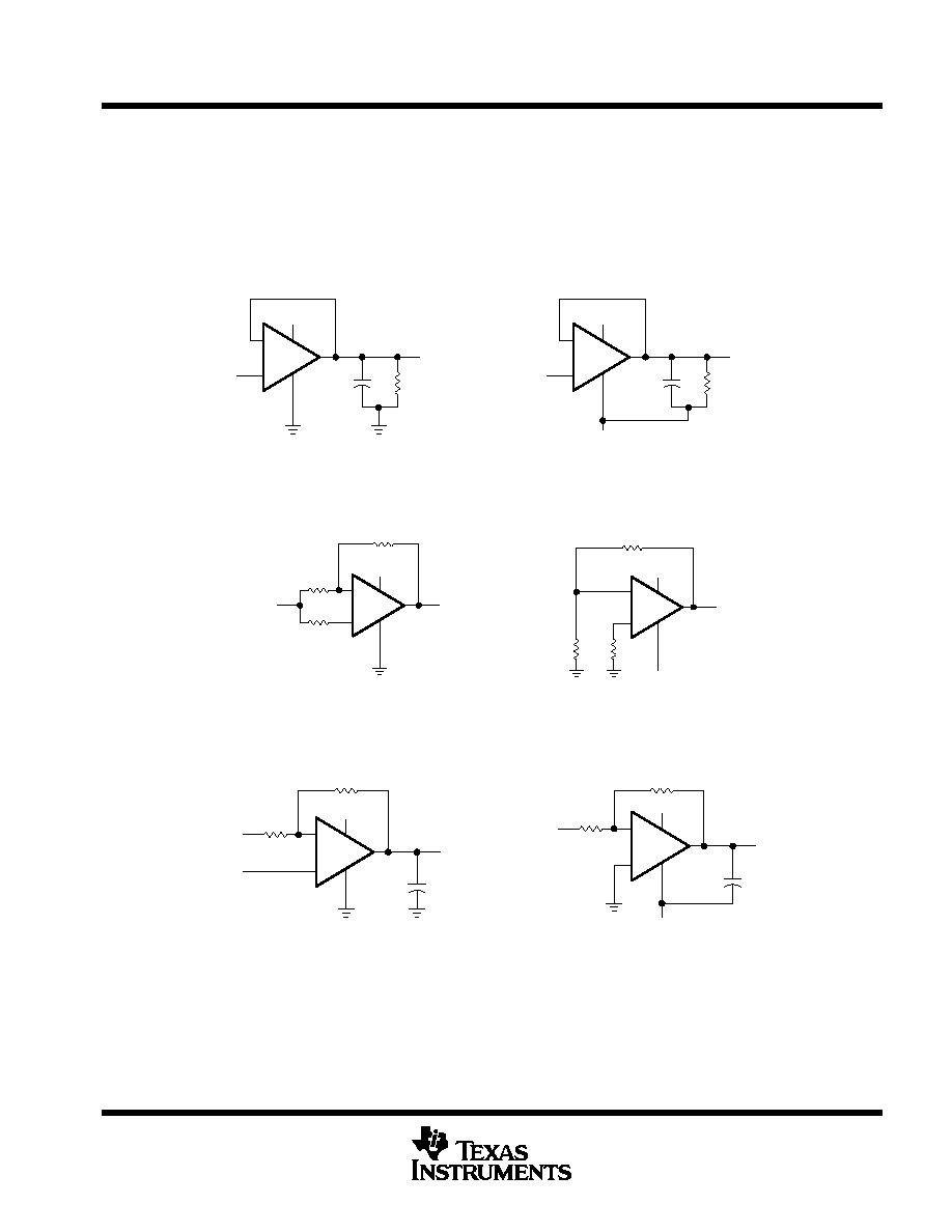
PARAMETER MEASUREMENT INFORMATION
single-supply versus split-supply test circuits
Because the TLC27L4 and TLC27L9 are optimized for single-supply operation, circuit configurations used for
the various tests often present some inconvenience since the input signal, in many cases, must be offset from
ground. This inconvenience can be avoided by testing the device with split supplies and the output load tied to
the negative rail. A comparison of single-supply versus split-supply test circuits is shown below. The use of either
circuit gives the same result.
≠
+
VDD
CL
RL
VO
VI
VI
VO
RL
CL
≠
+
VDD +
VDD ≠
(a) SINGLE SUPPLY
(b) SPLIT SUPPLY
Figure 1. Unity-Gain Amplifier
VDD
≠
+
VDD +
≠
+
1/2 VDD
20
VO
2 k
20
VDD ≠
20
20
2 k
VO
(b) SPLIT SUPPLY
(a) SINGLE SUPPLY
Figure 2. Noise-Test Circuit
VDD
≠
+
10 k
VO
100
CL
1/2 VDD
VI
VI
CL
100
VO
10 k
≠
+
VDD +
VDD ≠
(b) SPLIT SUPPLY
(a) SINGLE SUPPLY
Figure 3. Gain-of-100 Inverting Amplifier
TLC27L4, TLC27L4A, TLC27L4B, TLC27L4Y, TLC27L9
LinCMOS
TM
PRECISION QUAD OPERATIONAL AMPLIFIERS
SLOS053C ≠ OCTOBER 1987 ≠ REVISED AUGUST 1994
18
POST OFFICE BOX 655303
∑
DALLAS, TEXAS 75265
PARAMETER MEASUREMENT INFORMATION
input bias current
Because of the high input impedance of the TLC27L4 and TLC27L9 operational amplifiers, attempts to measure
the input bias current can result in erroneous readings. The bias current at normal room ambient temperature
is typically less than 1 pA, a value that is easily exceeded by leakages on the test socket. Two suggestions are
offered to avoid erroneous measurements:
1.
Isolate the device from other potential leakage sources. Use a grounded shield around and between the
device inputs (see Figure 4). Leakages that would otherwise flow to the inputs are shunted away.
2.
Compensate for the leakage of the test socket by actually performing an input bias current test (using
a picoammeter) with no device in the test socket. The actual input bias current can then be calculated
by subtracting the open-socket leakage readings from the readings obtained with a device in the test
socket.
One word of caution: many automatic testers as well as some bench-top operational amplifier testers use the
servo-loop technique with a resistor in series with the device input to measure the input bias current (the voltage
drop across the series resistor is measured and the bias current is calculated). This method requires that a
device be inserted into the test socket to obtain a correct reading; therefore, an open-socket reading is not
feasible using this method.
V = VIC
14
8
1
7
Figure 4. Isolation Metal Around Device Inputs (J and N packages)
low-level output voltage
To obtain low-supply-voltage operation, some compromise was necessary in the input stage. This compromise
results in the device low-level output being dependent on both the common-mode input voltage level as well
as the differential input voltage level. When attempting to correlate low-level output readings with those quoted
in the electrical specifications, these two conditions should be observed. If conditions other than these are to
be used, please refer to Figures 14 through 19 in the Typical Characteristics of this data sheet.
input offset voltage temperature coefficient
Erroneous readings often result from attempts to measure temperature coefficient of input offset voltage. This
parameter is actually a calculation using input offset voltage measurements obtained at two different
temperatures. When one (or both) of the temperatures is below freezing, moisture can collect on both the device
and the test socket. This moisture results in leakage and contact resistance, which can cause erroneous input
offset voltage readings. The isolation techniques previously mentioned have no effect on the leakage since the
moisture also covers the isolation metal itself, thereby rendering it useless. It is suggested that these
measurements be performed at temperatures above freezing to minimize error.
TLC27L4, TLC27L4A, TLC27L4B, TLC27L4Y, TLC27L9
LinCMOS
TM
PRECISION QUAD OPERATIONAL AMPLIFIERS
SLOS053C ≠ OCTOBER 1987 ≠ REVISED AUGUST 1994
19
POST OFFICE BOX 655303
∑
DALLAS, TEXAS 75265
PARAMETER MEASUREMENT INFORMATION
full-power response
Full-power response, the frequency above which the operational amplifier slew rate limits the output voltage
swing, is often specified two ways: full-linear response and full-peak response. The full-linear response is
generally measured by monitoring the distortion level of the output while increasing the frequency of a sinusoidal
input signal until the maximum frequency is found above which the output contains significant distortion. The
full-peak response is defined as the maximum output frequency, without regard to distortion, above which full
peak-to-peak output swing cannot be maintained.
Because there is no industry-wide accepted value for significant distortion, the full-peak response is specified
in this data sheet and is measured using the circuit of Figure 1. The initial setup involves the use of a sinusoidal
input to determine the maximum peak-to-peak output of the device (the amplitude of the sinusoidal wave is
increased until clipping occurs). The sinusoidal wave is then replaced with a square wave of the same
amplitude. The frequency is then increased until the maximum peak-to-peak output can no longer be maintained
(Figure 5). A square wave is used to allow a more accurate determination of the point at which the maximum
peak-to-peak output is reached.
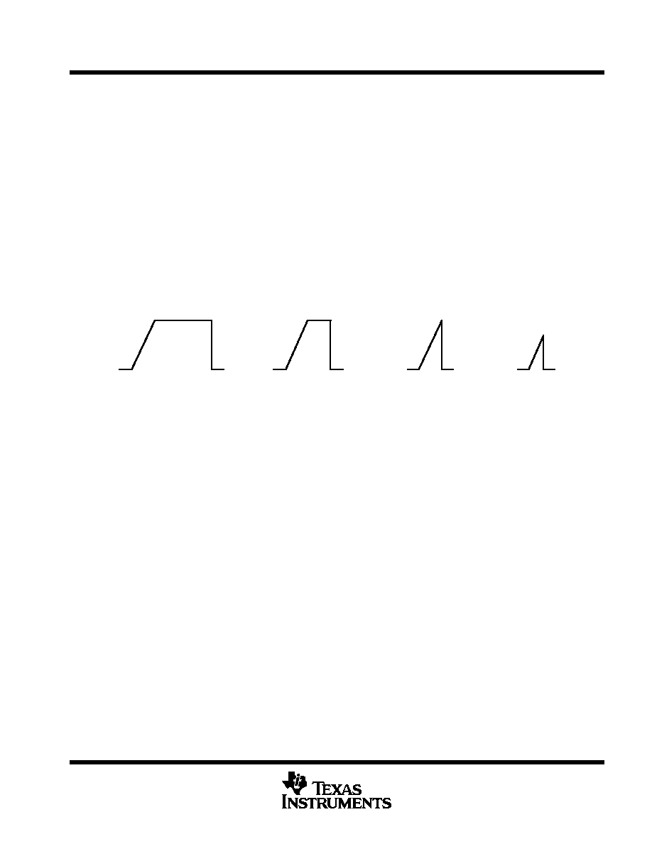
(a) f = 100 Hz
(b) BOM > f > 100 Hz
(c) f = BOM
(d) f > BOM
Figure 5. Full-Power-Response Output Signal
test time
Inadequate test time is a frequent problem, especially when testing CMOS devices in a high-volume,
short-test-time environment. Internal capacitances are inherently higher in CMOS than in bipolar and BiFET
devices and require longer test times than their bipolar and BiFET counterparts. The problem becomes more
pronounced with reduced supply levels and lower temperatures.
TLC27L4, TLC27L4A, TLC27L4B, TLC27L4Y, TLC27L9
LinCMOS
TM
PRECISION QUAD OPERATIONAL AMPLIFIERS
SLOS053C ≠ OCTOBER 1987 ≠ REVISED AUGUST 1994
20
POST OFFICE BOX 655303
∑
DALLAS, TEXAS 75265
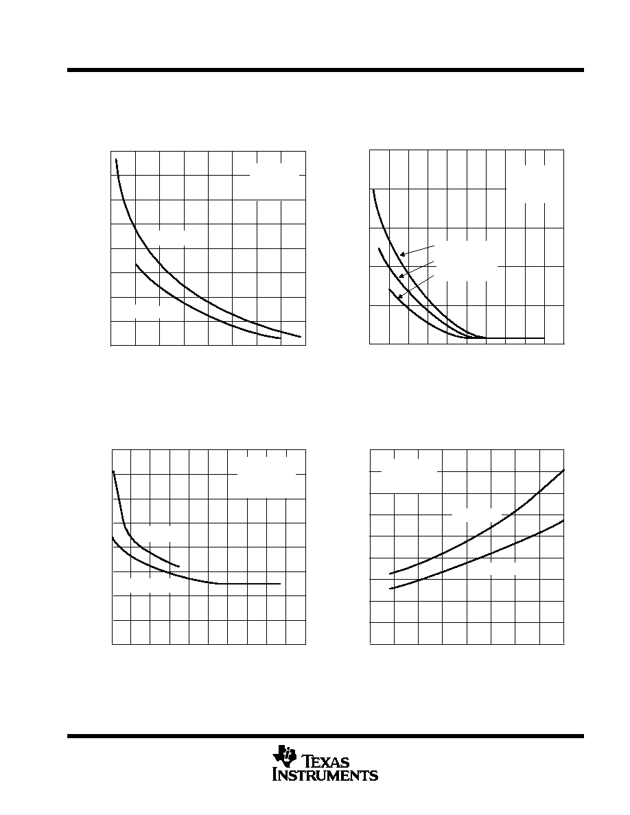
TYPICAL CHARACTERISTICS
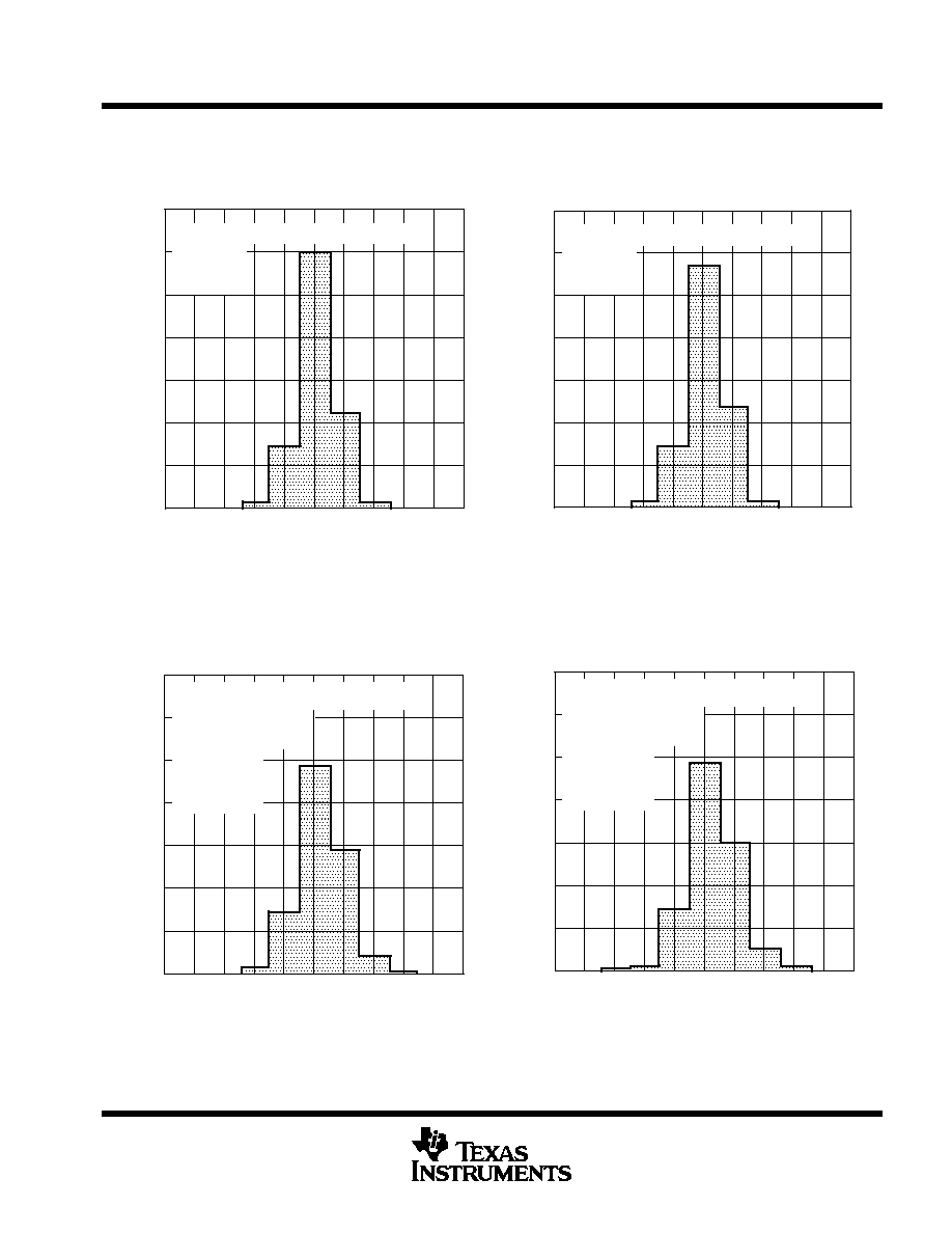
Table of Graphs
FIGURE
VIO
Input offset voltage
Distribution
6, 7
VIO
Temperature coefficient
Distribution
8, 9
vs High-level output current
10, 11
VOH
High-level output voltage
g
vs Supply voltage
,
12
OH
g
g
g
vs Free-air temperature
13
vs Common-mode input voltage
14, 15
VOL
Low level output voltage
vs Common mode in ut voltage
vs Differential input voltage
14, 15
16
VOL
Low-level output voltage
g
vs Free-air temperature
17
vs Low-level output current
18, 19
vs Supply voltage
20
AVD
Differential voltage amplification
y
g
vs Free-air temperature
21
VD
g
vs Frequency
32, 33
IIB / IIO
Input bias and input offset current
vs Free-air temperature
22
VIC
Common-mode input voltage
vs Supply voltage
23
IDD
Supply current
vs Supply voltage
24
IDD
Supply current
y
g
vs Free-air temperature
25
SR
Slew rate
vs Supply voltage
26
SR
Slew rate
y
g
vs Free-air temperature
27
Normalized slew rate
vs Free-air temperature
28
VO(PP)
Maximum peak-to-peak output voltage
vs Frequency
29
B1
Unity gain bandwidth
vs Free-air temperature
30
B1
Unity-gain bandwidth
vs Supply voltage
31
vs Supply voltage
34
m
Phase margin
y
g
vs Free-air temperature
35
m
g
vs Capacitive loads
36
Vn
Equivalent input noise voltage
vs Frequency
37
Phase shift
vs Frequency
32, 33
TLC27L4, TLC27L4A, TLC27L4B, TLC27L4Y, TLC27L9
LinCMOS
TM
PRECISION QUAD OPERATIONAL AMPLIFIERS
SLOS053C ≠ OCTOBER 1987 ≠ REVISED AUGUST 1994
21
POST OFFICE BOX 655303
∑
DALLAS, TEXAS 75265
TYPICAL CHARACTERISTICS
Figure 6
≠ 5
0
Percentage of Units ≠ %
VIO ≠ Input Offset Voltage ≠ mV
5
70
≠ 4
≠ 3
≠ 2
≠ 1
0
1
2
3
4
10
20
30
40
50
60
905 Amplifiers Tested From 6 Wafer Lots
VDD = 5 V
TA = 25
∞
C
N Package
DISTRIBUTION OF TLC27L4
INPUT OFFSET VOLTAGE
Figure 7
N Package
TA = 25
∞
C
VDD = 10 V
905 Amplifiers Tested From 6 Wafer Lots
60
50
40
30
20
10
4
3
2
1
0
≠ 1
≠ 2
≠ 3
≠ 4
70
5
VIO ≠ Input Offset Voltage ≠ mV
Percentage of Units ≠ %
0
≠ 5
DISTRIBUTION OF TLC27L4
INPUT OFFSET VOLTAGE
Figure 8
(1) 12.1
µ
V/
∞
C
(1) 19.2
µ
V/
∞
C
Outliers:
N Package
TA = 25
∞
C to 125
∞
C
VDD = 5 V
356 Amplifiers Tested From 8 Wafer Lots
60
50
40
30
20
10
8
6
4
2
0
≠ 2
≠ 4
≠ 6
≠ 8
70
10
VIO ≠ Temperature Coefficient ≠
µ
V/
∞
C
Percentage of Units ≠ %
0
≠ 10
DISTRIBUTION OF TLC27L4 AND TLC27L9
INPUT OFFSET VOLTAGE
TEMPERATURE COEFFICIENT
Figure 9
≠ 10
0
Percentage of Units ≠ %
VIO ≠ Temperature Coefficient ≠
µ
V/
∞
C
10
70
≠ 8
≠ 6
≠ 4
≠ 2
0
2
4
6
8
10
20
30
40
50
60
356 Amplifiers Tested From 6 Wafer Lots
VDD = 10 V
TA = 25
∞
C to 125
∞
C
N Package
Outliers:
(1) 18.7
µ
V/
∞
C
(1) 11.6
µ
V/
∞
C
DISTRIBUTION OF TLC27L4 AND TLC27L9
INPUT OFFSET VOLTAGE
TEMPERATURE COEFFICIENT
TLC27L4, TLC27L4A, TLC27L4B, TLC27L4Y, TLC27L9
LinCMOS
TM
PRECISION QUAD OPERATIONAL AMPLIFIERS
SLOS053C ≠ OCTOBER 1987 ≠ REVISED AUGUST 1994
22
POST OFFICE BOX 655303
∑
DALLAS, TEXAS 75265
TYPICAL CHARACTERISTICS
Figure 10
0
0
IOH ≠ High-Level Output Current ≠ mA
≠ 10
5
≠ 2
≠ 4
≠ 6
≠ 8
1
2
3
4
VID = 100 mV
TA = 25
∞
C
VDD = 5 V
VDD = 3 V
VDD = 4 V
HIGH-LEVEL OUTPUT VOLTAGE
vs
HIGH-LEVEL OUTPUT CURRENT
≠ High-Level Output V
oltage ≠ V
V
OH
Figure 11
0
0
IOH ≠ High-Level Output Current ≠ mA
≠ 40
16
≠ 10
≠ 20
≠ 30
2
4
6
8
10
12
14
TA = 25
∞
C
VID = 100 mV
VDD = 16 V
VDD = 10 V
HIGH-LEVEL OUTPUT VOLTAGE
vs
HIGH-LEVEL OUTPUT CURRENT
≠ High-Level Output V
oltage ≠ V
V
OH
≠ 35
≠ 5
≠ 15
≠ 25
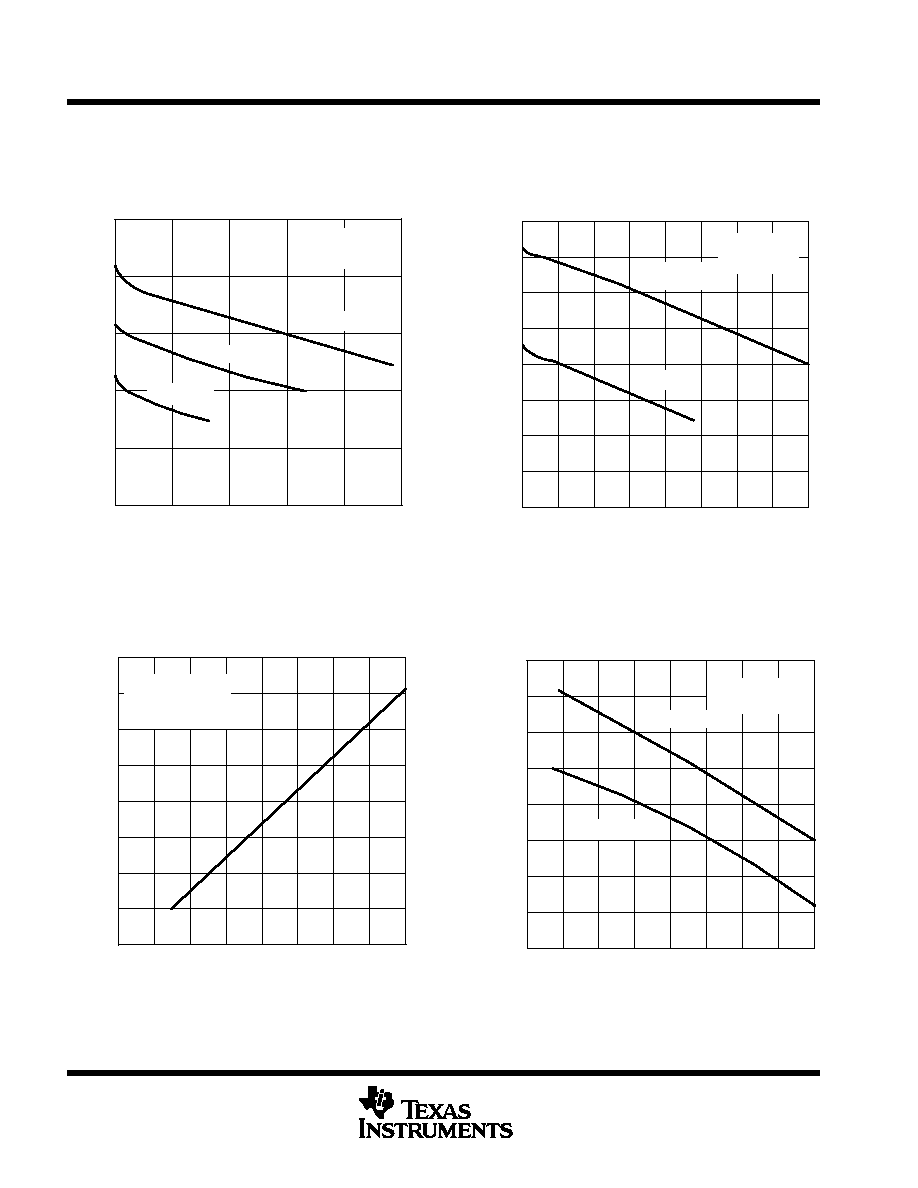
Figure 12
0
VDD ≠ Supply Voltage ≠ V
16
2
4
6
8
10
12
14
14
12
10
8
6
4
2
16
0
VID = 100 mV
RL = 1 M
TA = 25
∞
C
HIGH-LEVEL OUTPUT VOLTAGE
vs
SUPPLY VOLTAGE
≠ High-Level Output V
oltage ≠ V
V
OH
Figure 13
VDD ≠ 1.7
VDD ≠ 1.8
VDD ≠ 1.9
VDD ≠ 2
VDD ≠ 2.1
VDD ≠ 2.2
VDD ≠ 2.3
100
75
50
25
0
≠ 25
≠ 50
VDD ≠ 1.6
125
TA ≠ Free-Air Temperature ≠
∞
C
VDD ≠ 2.4
≠ 75
IOH = ≠ 5 mA
VID = 100 mV
VDD = 5 V
VDD = 10 V
HIGH-LEVEL OUTPUT VOLTAGE
vs
FREE-AIR TEMPERATURE
≠ High-Level Output V
oltage ≠ V
V
OH
Data at high and low temperatures are applicable only within the rated operating free-air temperature ranges of the various devices.
TLC27L4, TLC27L4A, TLC27L4B, TLC27L4Y, TLC27L9
LinCMOS
TM
PRECISION QUAD OPERATIONAL AMPLIFIERS
SLOS053C ≠ OCTOBER 1987 ≠ REVISED AUGUST 1994
23
POST OFFICE BOX 655303
∑
DALLAS, TEXAS 75265
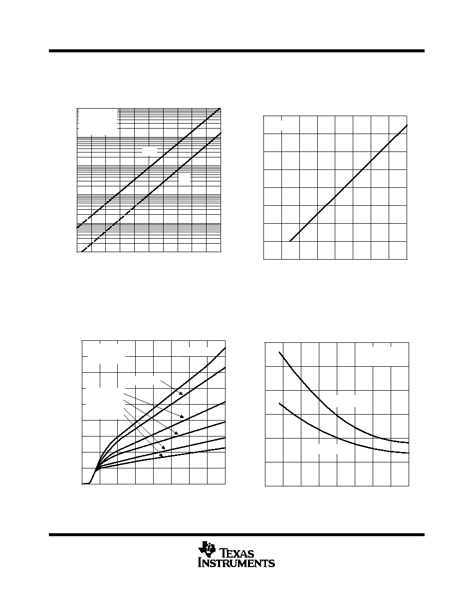
TYPICAL CHARACTERISTICS
Figure 14
0
300
≠ Low-Level Output V
oltage ≠ mV
VIC ≠ Common-Mode Input Voltage ≠ V
4
700
1
2
3
400
500
600
TA = 25
∞
C
IOL = 5 mA
VDD = 5 V
VID = ≠ 100 mV
VID = ≠ 1 V
LOW-LEVEL OUTPUT VOLTAGE
vs
COMMON-MODE INPUT VOLTAGE
V
OL
350
450
550
650
0.5
1.5
2.5
3.5
Figure 15
250
0
VIC ≠ Common-Mode Input Voltage ≠ V
300
350
400
450
500
2
4
6
8
10
VDD = 10 V
IOL = 5 mA
TA = 25
∞
C
VID = ≠ 1 V
VID = ≠ 2.5 V
VID = ≠ 100 mV
LOW-LEVEL OUTPUT VOLTAGE
vs
COMMON-MODE INPUT VOLTAGE
≠ Low-Level Output V
oltage ≠ mV
V
OL
7
1
3
5
9
Figure 16
LOW-LEVEL OUTPUT VOLTAGE
vs
DIFFERENTIAL INPUT VOLTAGE
0
VID ≠ Differential Input Voltage ≠ V
≠ 10
≠ 2
≠ 4
≠ 6
≠ 8
800
700
600
500
400
300
200
100
0
IOL = 5 mA
VIC = | VID/2 |
TA = 25
∞
C
VDD = 5 V
VDD = 10 V
≠ Low-Level Output V
oltage ≠ mV
V
OL
Figure 17
LOW-LEVEL OUTPUT VOLTAGE
vs
FREE-AIR TEMPERATURE
≠ 75
0
125
900
≠ 50
≠ 25
0
25
50
75
100
100
200
300
400
500
600
700
800
VIC = 0.5 V
VID = ≠ 1 V
IOL = 5 mA
VDD = 5 V
VDD = 10 V
TA ≠ Free-Air Temperature ≠
∞
C
≠ Low-Level Output V
oltage ≠ mV
V
OL
Data at high and low temperatures are applicable only within the rated operating free-air temperature ranges of the various devices.
TLC27L4, TLC27L4A, TLC27L4B, TLC27L4Y, TLC27L9
LinCMOS
TM
PRECISION QUAD OPERATIONAL AMPLIFIERS
SLOS053C ≠ OCTOBER 1987 ≠ REVISED AUGUST 1994
24
POST OFFICE BOX 655303
∑
DALLAS, TEXAS 75265
TYPICAL CHARACTERISTICS
Figure 18
0
IOL ≠ Low-Level Output Current ≠ mA
1
8
0
1
2
3
4
5
6
7
0.1
0.2
0.3
0.4
0.5
0.6
0.7
0.8
0.9
VID = ≠ 1 V
VIC = 0.5 V
TA = 25
∞
C
VDD = 3 V
VDD = 4 V
VDD = 5 V
LOW-LEVEL OUTPUT VOLTAGE
vs
LOW-LEVEL OUTPUT CURRENT
≠ Low-Level Output V
oltage ≠ V
V
OL
Figure 19
0
IOL ≠ Low-Level Output Current ≠ mA
3
30
0
5
10
15
20
25
0.5
1
1.5
2
2.5
TA = 25
∞
C
VIC = 0.5 V
VID = ≠ 1 V
VDD = 10 V
VDD = 16 V
LOW-LEVEL OUTPUT VOLTAGE
vs
LOW-LEVEL OUTPUT CURRENT
≠ Low-Level Output V
oltage ≠ V
V
OL
Figure 20
0
VDD ≠ Supply Voltage ≠ V
2000
0
2
4
6
8
10
12
14
200
400
600
800
1000
1200
1400
1600
1800
RL = 1 M
TA = ≠ 55
∞
C
TA = ≠ 40
∞
C
TA = 0
∞
C
TA = 25
∞
C
TA = 70
∞
C
TA = 85
∞
C
TA = 125
∞
C
LARGE-SIGNAL
DIFFERENTIAL VOLTAGE AMPLIFICATION
vs
SUPPLY VOLTAGE
A
VD ≠ Large-Signal Differential
¡¡
¡¡
A
VD
V
oltage
Amplification ≠ V/mV
16
Figure 21
100
75
50
25
0
≠ 25
≠ 50
0
125
TA ≠ Free-Air Temperature ≠
∞
C
≠ 75
RL = 1 M
VDD = 5 V
VDD = 10 V
1800
1600
1400
1200
1000
800
600
400
200
2000
LARGE-SIGNAL
DIFFERENTIAL VOLTAGE AMPLIFICATION
vs
FREE-AIR TEMPERATURE
A
VD ≠ Large-Signal Differential
¡¡
¡¡
¡¡
A
VD
V
oltage
Amplification ≠ V/mV
Data at high and low temperatures are applicable only within the rated operating free-air temperature ranges of the various devices.
TLC27L4, TLC27L4A, TLC27L4B, TLC27L4Y, TLC27L9
LinCMOS
TM
PRECISION QUAD OPERATIONAL AMPLIFIERS
SLOS053C ≠ OCTOBER 1987 ≠ REVISED AUGUST 1994
25
POST OFFICE BOX 655303
∑
DALLAS, TEXAS 75265
TYPICAL CHARACTERISTICS
Figure 22
0.1
125
10000
45
65
85
105
1
10
100
1000
25
TA ≠ Free-Air Temperature ≠
∞
C
VDD = 10 V
VIC = 5 V
See Note A
IIB
IIO
INPUT BIAS CURRENT AND INPUT OFFSET CURRENT
vs
FREE-AIR TEMPERATURE
≠ Input Bias and Offset Currents ≠ pA
I IB
I IO
and
NOTE A: The typical values of input bias current and input offset
current below 5 pA were determined mathematically.
Figure 23
0
VDD ≠ Supply Voltage ≠ V
16
16
0
2
4
6
8
10
12
14
2
4
6
8
10
12
14
TA = 25
∞
C
COMMON-MODE
INPUT VOLTAGE POSITIVE LIMIT
vs
SUPPLY VOLTAGE
IC
V
≠
Common-Mode Input V
oltage ≠ V
Figure 24
No Load
VO = VDD/2
0
VDD ≠ Supply Voltage ≠ V
180
16
0
2
4
6
8
10
12
14
20
40
60
80
100
120
140
160
ÃÃÃÃ
ÃÃÃÃ
TA = ≠ 40
∞
C
SUPPLY CURRENT
vs
SUPPLY VOLTAGE
≠ Supply Current ≠
I DD
A
µ
ÃÃÃÃ
ÃÃÃÃ
ÃÃÃÃ
ÃÃÃÃ
TA = 0
∞
C
TA = 25
∞
C
TA = 70
∞
C
TA = 125
∞
C
ÃÃÃÃ
ÃÃÃÃ
TA = ≠ 55
∞
C
Figure 25
VO = VDD/2
No Load
VDD = 10 V
VDD = 5 V
≠ 75
TA ≠ Free-Air Temperature ≠
∞
C
120
125
0
≠ 50
≠ 25
0
25
50
75
100
20
40
60
80
100
SUPPLY CURRENT
vs
FREE-AIR TEMPERATURE
≠ Supply Current ≠
I DD
A
µ
Data at high and low temperatures are applicable only within the rated operating free-air temperature ranges of the various devices.
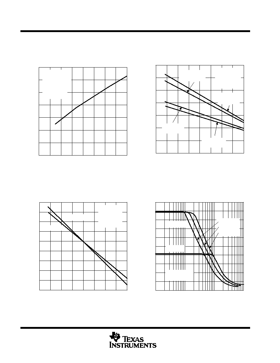
TLC27L4, TLC27L4A, TLC27L4B, TLC27L4Y, TLC27L9
LinCMOS
TM
PRECISION QUAD OPERATIONAL AMPLIFIERS
SLOS053C ≠ OCTOBER 1987 ≠ REVISED AUGUST 1994
26
POST OFFICE BOX 655303
∑
DALLAS, TEXAS 75265
TYPICAL CHARACTERISTICS
Figure 26
CL = 20 pF
RL = 1 m
VIPP = 1 V
AV = 1
See Figure 1
TA = 25
∞
C
0
VDD ≠ Supply Voltage ≠ V
0.07
16
0.00
2
4
6
8
10
12
14
0.01
0.02
0.03
0.04
0.05
0.06
SLEW RATE
vs
SUPPLY VOLTAGE
µ
s
SR ≠ Slew Rate ≠ V/
Figure 27
VIPP = 5.5 V
VDD = 10 V
VDD = 5 V
VIPP = 1 V
VDD = 5 V
VIPP = 2.5 V
VDD = 10 V
VIPP = 1 V
≠ 75
TA ≠ Free-Air Temperature ≠
∞
C
0.07
125
0.00
≠ 50
≠ 25
0
25
50
75
100
0.01
0.02
0.03
0.04
0.05
0.06
CL = 20 pF
RL = 1 M
See Figure 1
AV = 1
SLEW RATE
vs
FREE-AIR TEMPERATURE
µ
s
SR ≠ Slew Rate ≠ V/
Figure 28
≠ 75
Normalized Slew Rate
TA ≠ Free-Air Temperature ≠
∞
C
1.4
125
0.5
≠ 50
≠ 25
0
25
50
75
100
0.6
0.7
0.8
0.9
1
1.1
1.2
1.3
AV = 1
VIPP = 1 V
RL = 1 M
CL = 20 pF
VDD = 10 V
VDD = 5 V
NORMALIZED SLEW RATE
vs
FREE-AIR TEMPERATURE
Figure 29
0.1
f ≠ Frequency ≠ kHz
10
100
0
1
2
3
4
5
6
7
8
9
1
10
VDD = 10 V
VDD = 5 V
See Figure 1
RL = 1 M
TA = 125
∞
C
TA = 25
∞
C
TA = ≠ 55
∞
C
MAXIMUM PEAK-TO-PEAK OUTPUT VOLTAGE
vs
FREQUENCY
≠ Maximum Peak-to-Peak Output V
oltage ≠ V
V
O(PP)
Data at high and low temperatures are applicable only within the rated operating free-air temperature ranges of the various devices.
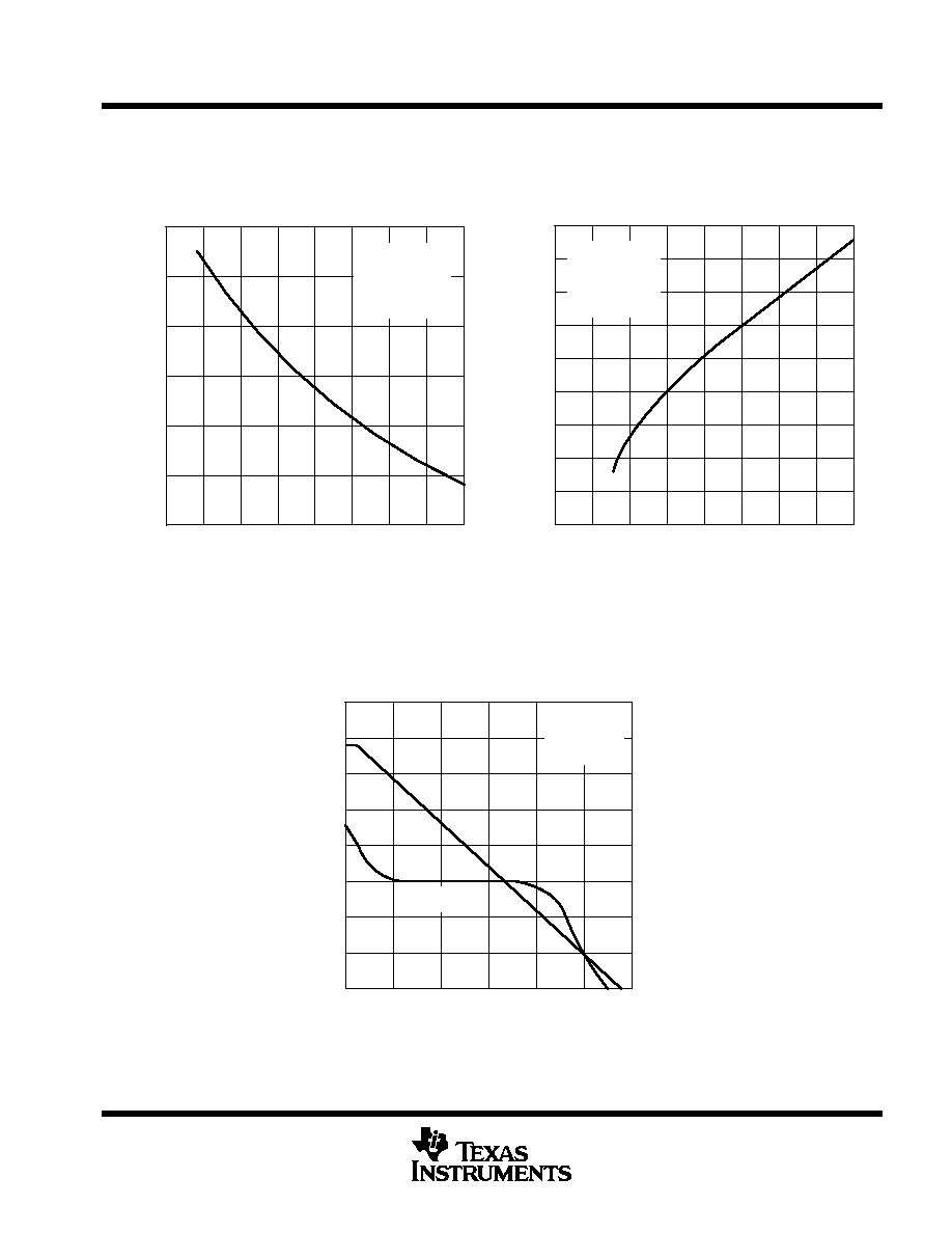
TLC27L4, TLC27L4A, TLC27L4B, TLC27L4Y, TLC27L9
LinCMOS
TM
PRECISION QUAD OPERATIONAL AMPLIFIERS
SLOS053C ≠ OCTOBER 1987 ≠ REVISED AUGUST 1994
27
POST OFFICE BOX 655303
∑
DALLAS, TEXAS 75265
TYPICAL CHARACTERISTICS
Figure 30
VDD = 5 V
VI = 10 mV
CL = 20 pF
See Figure 3
≠ 75
TA ≠ Free-Air Temperature ≠
∞
C
150
125
30
≠ 50
≠ 25
0
25
50
75
100
50
70
90
110
130
UNITY-GAIN BANDWIDTH
vs
FREE-AIR TEMPERATURE
≠ Unity-Gain Bandwidth ≠ kHz
B
1
Figure 31
0
VDD ≠ Supply Voltage ≠ V
140
16
50
2
4
6
8
10
12
14
60
70
80
90
100
110
120
130
See Figure 3
TA = 25
∞
C
CL = 20 pF
VI = 10 mV
UNITY-GAIN BANDWIDTH
vs
SUPPLY VOLTAGE
≠ Unity-Gain Bandwidth ≠ kHz
B
1
1
f ≠ Frequency ≠ Hz
1 M
0.1
10
100
1 k
10 k
100 k
1
101
102
103
104
105
106
150
∞
120
∞
90
∞
60
∞
30
∞
0
∞
180
∞
TA = 25
∞
C
RL = 1 M
VDD = 5 V
AVD
Phase Shift
107
LARGE-SIGNAL DIFFERENTIAL VOLTAGE
AMPLIFICATION AND PHASE SHIFT
vs
FREQUENCY
Phase Shift
A
VD ≠ Large-Signal Differential
¡¡
¡¡
¡¡
A
VD
V
oltage Amplification
Figure 32
Data at high and low temperatures are applicable only within the rated operating free-air temperature ranges of the various devices.
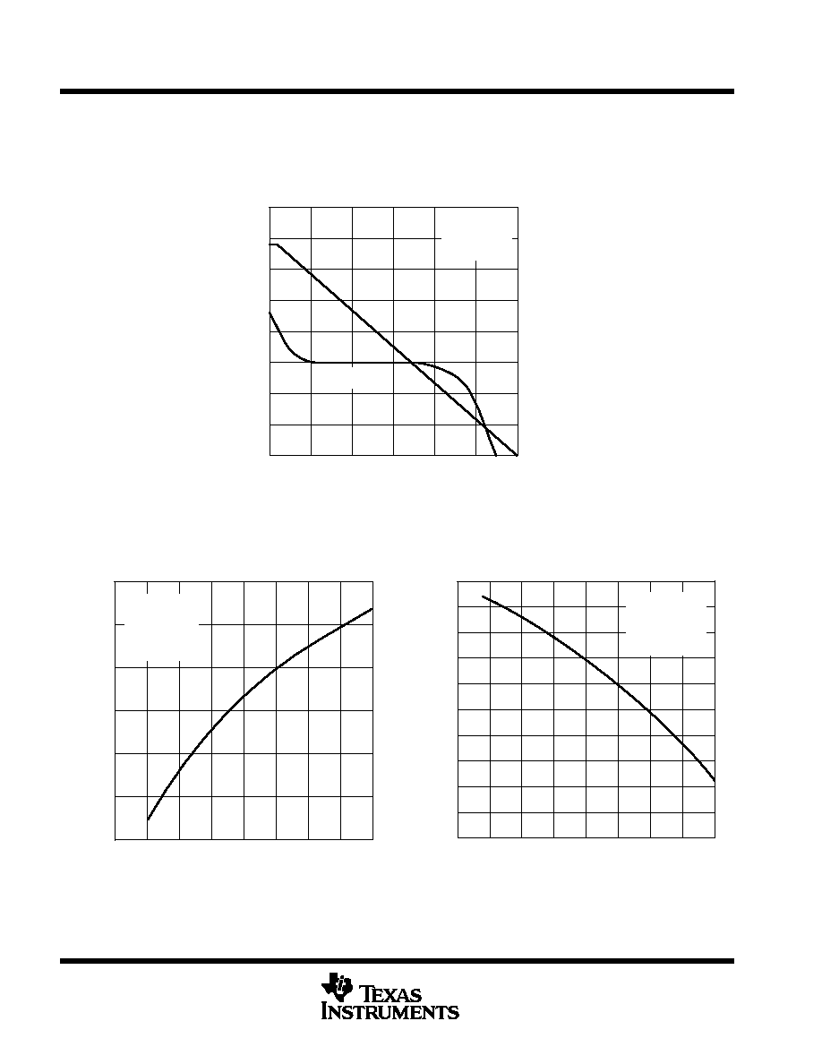
TLC27L4, TLC27L4A, TLC27L4B, TLC27L4Y, TLC27L9
LinCMOS
TM
PRECISION QUAD OPERATIONAL AMPLIFIERS
SLOS053C ≠ OCTOBER 1987 ≠ REVISED AUGUST 1994
28
POST OFFICE BOX 655303
∑
DALLAS, TEXAS 75265
TYPICAL CHARACTERISTICS
Phase Shift
AVD
VDD = 10 V
RL = 1 M
TA = 25
∞
C
180
∞
0
∞
30
∞
60
∞
90
∞
120
∞
150
∞
10 6
10 5
10 4
10 3
10 2
10 1
1
100 k
10 k
1 k
100
10
0.1
1 M
f ≠ Frequency ≠ Hz
1
10 7
LARGE-SIGNAL DIFFERENTIAL VOLTAGE
AMPLIFICATION AND PHASE SHIFT
vs
FREQUENCY
Phase Shift
A
VD ≠ Large-Signal Differential
¡
¡
¡
A
VD
V
oltage Amplification
Figure 33
Figure 34
0
VDD ≠ Supply Voltage ≠ V
42
∞
16
30
∞
2
4
6
8
10
12
14
32
∞
34
∞
36
∞
38
∞
40
∞
See Figure 3
VI = 10 mV
TA = 25
∞
C
CL = 20 pF
PHASE MARGIN
vs
SUPPLY VOLTAGE
≠ Phase Margin
m
Figure 35
See Figure 3
VI = 10 mV
CL = 20 pF
VDD = 5 mV
≠ 75
TA ≠ Free-Air Temperature ≠
∞
C
40
∞
125
20
∞
≠ 50
≠ 25
0
25
50
75
100
24
∞
28
∞
32
∞
36
∞
PHASE MARGIN
vs
FREE-AIR TEMPERATURE
≠ Phase Margin
m
30
∞
34
∞
38
∞
26
∞
22
∞
Data at high and low temperatures are applicable only within the rated operating free-air temperature ranges of the various devices.
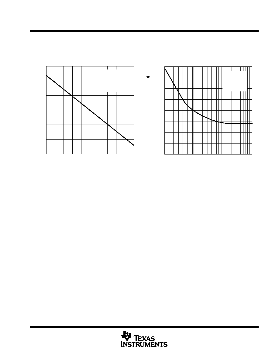
TLC27L4, TLC27L4A, TLC27L4B, TLC27L4Y, TLC27L9
LinCMOS
TM
PRECISION QUAD OPERATIONAL AMPLIFIERS
SLOS053C ≠ OCTOBER 1987 ≠ REVISED AUGUST 1994
29
POST OFFICE BOX 655303
∑
DALLAS, TEXAS 75265
TYPICAL CHARACTERISTICS
Figure 36
VDD = 5 mV
TA = 25
∞
C
See Figure 3
VI = 10 mV
0
CL ≠ Capacitive Load ≠ pF
37
∞
100
25
∞
20
40
60
80
27
∞
29
∞
31
∞
33
∞
35
∞
PHASE MARGIN
vs
CAPACITIVE LOAD
≠ Phase Margin
m
Figure 37
See Figure 2
TA = 25
∞
C
RS = 20
VDD = 5 V
1
f ≠ Frequency ≠ Hz
200
1000
0
25
50
75
100
125
150
175
10
100
EQUIVALENT INPUT NOISE VOLTAGE
vs
FREQUENCY
≠ Equivalent Input Noise V
oltage ≠
nV/
Hz
V
n
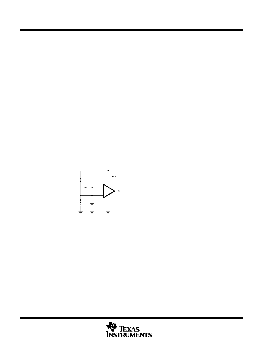
TLC27L4, TLC27L4A, TLC27L4B, TLC27L4Y, TLC27L9
LinCMOS
TM
PRECISION QUAD OPERATIONAL AMPLIFIERS
SLOS053C ≠ OCTOBER 1987 ≠ REVISED AUGUST 1994
30
POST OFFICE BOX 655303
∑
DALLAS, TEXAS 75265
APPLICATION INFORMATION
single-supply operation
While the TLC27L4 and TLC27L9 perform well using dual power supplies (also called balanced or split
supplies), the design is optimized for single-supply operation. This design includes an input common-mode
voltage range that encompasses ground as well as an output voltage range that pulls down to ground. The
supply voltage range extends down to 3 V (C-suffix types), thus allowing operation with supply levels commonly
available for TTL and HCMOS; however, for maximum dynamic range, 16-V single-supply operation is
recommended.
Many single-supply applications require that a voltage be applied to one input to establish a reference level that
is above ground. A resistive voltage divider is usually sufficient to establish this reference level (see Figure 38).
The low input bias current of the TLC27L4 and TLC27L9 permits the use of very large resistive values to
implement the voltage divider, thus minimizing power consumption.
The TLC27L4 and TLC27L9 work well in conjunction with digital logic; however, when powering both linear
devices and digital logic from the same power supply, the following precautions are recommended:
1.
Power the linear devices from separate bypassed supply lines (see Figure 39); otherwise, the linear
device supply rails can fluctuate due to voltage drops caused by high switching currents in the digital
logic.
2.
Use proper bypass techniques to reduce the probability of noise-induced errors. Single capacitive
decoupling is often adequate; however, high-frequency applications may require RC decoupling.
R4
VO
VDD
R2
R1
VI
VREF
R3
C
0.01
µ
F
≠
+
VREF = VDD
R3
R1 + R3
VO = (VREF ≠ VI )
R4
R2
+ VREF
Figure 38. Inverting Amplifier With Voltage Reference
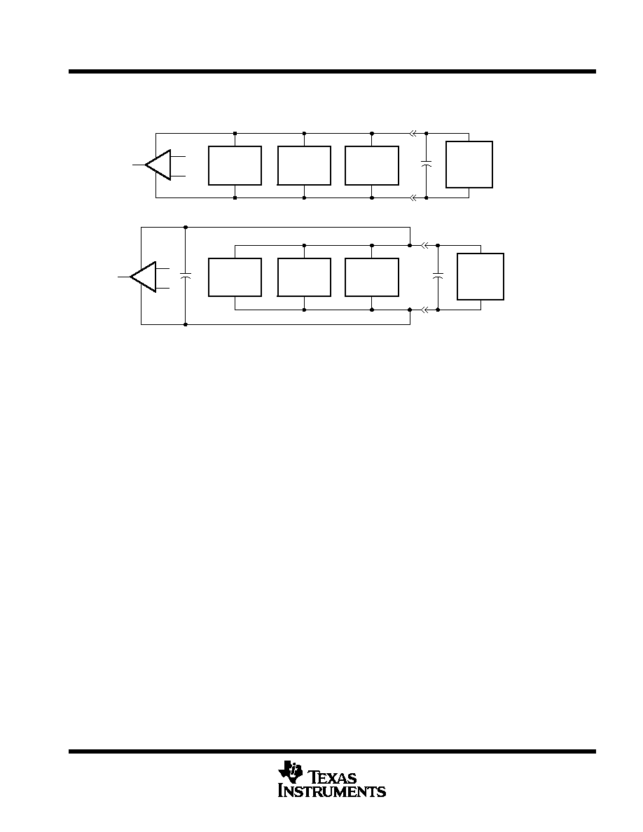
TLC27L4, TLC27L4A, TLC27L4B, TLC27L4Y, TLC27L9
LinCMOS
TM
PRECISION QUAD OPERATIONAL AMPLIFIERS
SLOS053C ≠ OCTOBER 1987 ≠ REVISED AUGUST 1994
31
POST OFFICE BOX 655303
∑
DALLAS, TEXAS 75265
APPLICATION INFORMATION
single-supply operation (continued)
Logic
Logic
Logic
≠
+
≠
+
(a) COMMON SUPPLY RAILS
(b) SEPARATE BYPASSED SUPPLY RAILS (preferred)
Logic
Logic
Logic
Power
Supply
Power
Supply
Output
Output
Figure 39. Common Versus Separate Supply Rails
input characteristics
The TLC27L4 and TLC27L9 are specified with a minimum and a maximum input voltage that, if exceeded at
either input, could cause the device to malfunction. Exceeding this specified range is a common problem,
especially in single-supply operation. Note that the lower range limit includes the negative rail, while the upper
range limit is specified at V
DD
≠ 1 V at T
A
= 25
∞
C and at V
DD
≠ 1.5 V at all other temperatures.
The use of the polysilicon-gate process and the careful input circuit design gives the TLC27L4 and TLC27L9
very good input offset voltage drift characteristics relative to conventional metal-gate processes. Offset voltage
drift in CMOS devices is highly influenced by threshold voltage shifts caused by polarization of the phosphorus
dopant implanted in the oxide. Placing the phosphorus dopant in a conductor (such as a polysilicon gate)
alleviates the polarization problem, thus reducing threshold voltage shifts by more than an order of magnitude.
The offset voltage drift with time has been calculated to be typically 0.1
µ
V/month, including the first month of
operation.
Because of the extremely high input impedance and resulting low bias current requirements, the TLC27L4 and
TLC27L9 are well suited for low-level signal processing; however, leakage currents on printed circuit boards
and sockets can easily exceed bias current requirements and cause a degradation in device performance. It
is good practice to include guard rings around inputs (similar to those of Figure 4 in the Parameter Measurement
Information section). These guards should be driven from a low-impedance source at the same voltage level
as the common-mode input (see Figure 40).
The inputs of any unused amplifiers should be tied to ground to avoid possible oscillation.
noise performance
The noise specifications in operational amplifier circuits are greatly dependent on the current in the first-stage
differential amplifier. The low input bias current requirements of the TLC27L4 and TLC27L9 result in a very low
noise current, which is insignificant in most applications. This feature makes the devices especially favorable
over bipolar devices when using values of circuit impedance greater than 50 k
, since bipolar devices exhibit
greater noise currents.
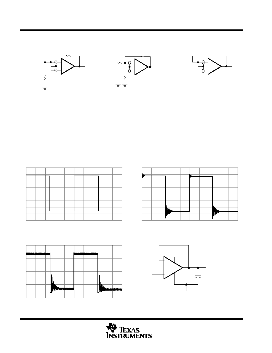
TLC27L4, TLC27L4A, TLC27L4B, TLC27L4Y, TLC27L9
LinCMOS
TM
PRECISION QUAD OPERATIONAL AMPLIFIERS
SLOS053C ≠ OCTOBER 1987 ≠ REVISED AUGUST 1994
32
POST OFFICE BOX 655303
∑
DALLAS, TEXAS 75265
APPLICATION INFORMATION
noise performance (continued)
VI
(a) NONINVERTING AMPLIFIER
(c) UNITY-GAIN AMPLIFIER
≠
+
(b) INVERTING AMPLIFIER
VI
≠
+
≠
+
VI
VO
VO
VO
Figure 40. Guard-Ring Schemes
output characteristics
The output stage of the TLC27L4 and TLC27L9 is designed to sink and source relatively high amounts of current
(see typical characteristics). If the output is subjected to a short-circuit condition, this high current capability can
cause device damage under certain conditions. Output current capability increases with supply voltage.
All operating characteristics of the TLC27L4 and TLC27L9 were measured using a 20-pF load. The devices
drive higher capacitive loads; however, as output load capacitance increases, the resulting response pole
occurs at lower frequencies, thereby causing ringing, peaking, or even oscillation (see Figure 41). In many
cases, adding a small amount of resistance in series with the load capacitance alleviates the problem.
≠
+
2.5 V
VO
CL
≠ 2.5 V
VI
(a) CL = 20 pF, RL = NO LOAD
(b) CL = 260 pF, RL = NO LOAD
(c) CL = 310 pF, RL = NO LOAD
(d) TEST CIRCUIT
TA = 25
∞
C
f = 1 kHz
VIPP = 1 V
Figure 41. Effect of Capacitive Loads and Test Circuit
TLC27L4, TLC27L4A, TLC27L4B, TLC27L4Y, TLC27L9
LinCMOS
TM
PRECISION QUAD OPERATIONAL AMPLIFIERS
SLOS053C ≠ OCTOBER 1987 ≠ REVISED AUGUST 1994
33
POST OFFICE BOX 655303
∑
DALLAS, TEXAS 75265
APPLICATION INFORMATION
output characteristics (continued)
Although the TLC27L4 and TLC27L9 possess excellent high-level output voltage and current capability,
methods for boosting this capability are available, if needed. The simplest method involves the use of a pullup
resistor (Rb) connected from the output to the positive supply rail (see Figure 42). There are two disadvantages
to the use of this circuit. First, the NMOS pulldown transistor N4 (see equivalent schematic) must sink a
comparatively large amount of current. In this circuit, N4 behaves like a linear resistor with an on-resistance
between approximately 60
and 180
, depending on how hard the operational amplifier input is driven. With
very low values of R
P
, a voltage offset from 0 V at the output occurs. Second, pullup resistor R
P
acts as a drain
load to N4 and the gain of the operational amplifier is reduced at output voltage levels where N5 is not supplying
the output current.
Figure 42. Resistive Pullup to Increase V
OH
≠
+
VI
VDD
RP
VO
R2
R1
RL
IP
IF
IL
IP = Pullup current
required by the
operational amplifier
(typically 500
µ
A)
Rp =
VDD ≠ VO
IF + IL + IP
Figure 43. Compensation for
Input Capacitance
≠
+
C
VO
feedback
Operational amplifier circuits nearly always employ feedback, and since feedback is the first prerequisite for
oscillation, some caution is appropriate. Most oscillation problems result from driving capacitive loads
(discussed previously) and ignoring stray input capacitance. A small-value capacitor connected in parallel with
the feedback resistor is an effective remedy (see Figure 43). The value of this capacitor is optimized empirically.
electrostatic discharge protection
The TLC27L4 and TLC27L9 incorporate an internal electrostatic discharge (ESD) protection circuit that
prevents functional failures at voltages up to 2000 V as tested under MIL-STD-883C, Method 3015.2. Care
should be exercised, however, when handling these devices, as exposure to ESD may result in the degradation
of the device parametric performance. The protection circuit also causes the input bias currents to be
temperature dependent and have the characteristics of a reverse-biased diode.
latch-up
Because CMOS devices are susceptible to latch-up due to their inherent parasitic thyristors, the TLC27L4 and
TLC27L9 inputs and outputs were designed to withstand ≠ 100-mA surge currents without sustaining latch-up;
however, techniques should be used to reduce the chance of latch-up whenever possible. Internal protection
diodes should not, by design, be forward biased. Applied input and output voltage should not exceed the supply
voltage by more than 300 mV. Care should be exercised when using capacitive coupling on pulse generators.
Supply transients should be shunted by the use of decoupling capacitors (0.1
µ
F typical) located across the
supply rails as close to the device as possible.
TLC27L4, TLC27L4A, TLC27L4B, TLC27L4Y, TLC27L9
LinCMOS
TM
PRECISION QUAD OPERATIONAL AMPLIFIERS
SLOS053C ≠ OCTOBER 1987 ≠ REVISED AUGUST 1994
34
POST OFFICE BOX 655303
∑
DALLAS, TEXAS 75265
APPLICATION INFORMATION
latch-up (continued)
The current path established if latch-up occurs is usually between the positive supply rail and ground and can
be triggered by surges on the supply lines and/or voltages on either the output or inputs that exceed the supply
voltage. Once latch-up occurs, the current flow is limited only by the impedance of the power supply and the
forward resistance of the parasitic thyristor and usually results in the destruction of the device. The chance of
latch-up occurring increases with increasing temperature and supply voltages.
≠
+
≠
+
500 k
500 k
5 V
500 k
0.1
µ
F
500 k
VO2
VO1
1/4
TLC27L4
TLC27L4
1/4
Figure 44. Multivibrator
TLC27L4
1/4
≠
+
100 k
VDD
33 k
100 k
100 k
Set
Reset
VO
NOTE: VDD = 5 V to 16 V
Figure 45. Set /Reset Flip-Flop
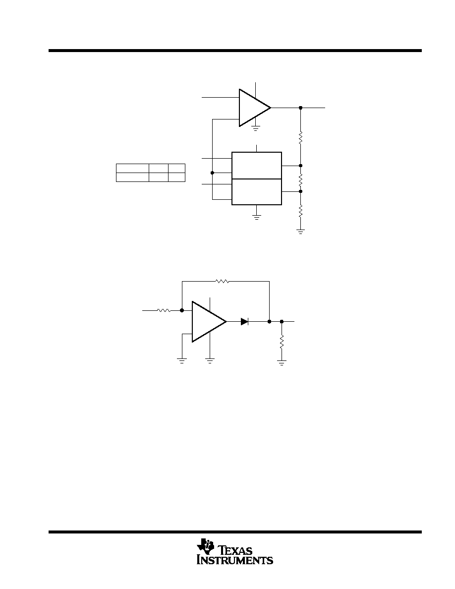
TLC27L4, TLC27L4A, TLC27L4B, TLC27L4Y, TLC27L9
LinCMOS
TM
PRECISION QUAD OPERATIONAL AMPLIFIERS
SLOS053C ≠ OCTOBER 1987 ≠ REVISED AUGUST 1994
35
POST OFFICE BOX 655303
∑
DALLAS, TEXAS 75265
APPLICATION INFORMATION
≠
+
VDD
VO
90 k
9 k
X1
1
1
B
TLC4066
VDD
VI
S1
S2
C
A
C
A
2
X2
2
B
1 k
Analog
Switch
1/4
TLC27L9
SELECT
AV
S1
S2
10
100
NOTE: VDD = 5 V to 12 V
Figure 46. Amplifier With Digital Gain Selection
≠
+
10 k
VO
100 k
VDD
20 k
VI
1/4
TLC27L4
NOTE: VDD = 5 V to 16 V
Figure 47. Full-Wave Rectifier
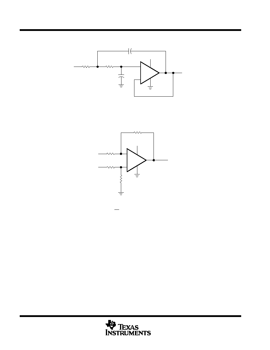
TLC27L4, TLC27L4A, TLC27L4B, TLC27L4Y, TLC27L9
LinCMOS
TM
PRECISION QUAD OPERATIONAL AMPLIFIERS
SLOS053C ≠ OCTOBER 1987 ≠ REVISED AUGUST 1994
36
POST OFFICE BOX 655303
∑
DALLAS, TEXAS 75265
APPLICATION INFORMATION
≠
+
5 V
0.016
µ
F
10 k
10 k
VO
0.016
µ
F
VI
1/4
TLC27L4
NOTE: Normalized to FC = 1 kHz and RL = 10 k
Figure 48. Two-Pole Low-Pass Butterworth Filter
VIA
VDD
≠
+
VIB
R2
100 k
10 k
R1
100 k
R2
TLC27L9
1/4
VO
R1
10 k
NOTE: VDD = 5 V to 16 V
V
O
+
R2
R1
V
IB
*
V
IA
Figure 49. Difference Amplifier

IMPORTANT NOTICE
Texas Instruments and its subsidiaries (TI) reserve the right to make changes to their products or to discontinue
any product or service without notice, and advise customers to obtain the latest version of relevant information
to verify, before placing orders, that information being relied on is current and complete. All products are sold
subject to the terms and conditions of sale supplied at the time of order acknowledgement, including those
pertaining to warranty, patent infringement, and limitation of liability.
TI warrants performance of its semiconductor products to the specifications applicable at the time of sale in
accordance with TI's standard warranty. Testing and other quality control techniques are utilized to the extent
TI deems necessary to support this warranty. Specific testing of all parameters of each device is not necessarily
performed, except those mandated by government requirements.
CERTAIN APPLICATIONS USING SEMICONDUCTOR PRODUCTS MAY INVOLVE POTENTIAL RISKS OF
DEATH, PERSONAL INJURY, OR SEVERE PROPERTY OR ENVIRONMENTAL DAMAGE ("CRITICAL
APPLICATIONS"). TI SEMICONDUCTOR PRODUCTS ARE NOT DESIGNED, AUTHORIZED, OR
WARRANTED TO BE SUITABLE FOR USE IN LIFE-SUPPORT DEVICES OR SYSTEMS OR OTHER
CRITICAL APPLICATIONS. INCLUSION OF TI PRODUCTS IN SUCH APPLICATIONS IS UNDERSTOOD TO
BE FULLY AT THE CUSTOMER'S RISK.
In order to minimize risks associated with the customer's applications, adequate design and operating
safeguards must be provided by the customer to minimize inherent or procedural hazards.
TI assumes no liability for applications assistance or customer product design. TI does not warrant or represent
that any license, either express or implied, is granted under any patent right, copyright, mask work right, or other
intellectual property right of TI covering or relating to any combination, machine, or process in which such
semiconductor products or services might be or are used. TI's publication of information regarding any third
party's products or services does not constitute TI's approval, warranty or endorsement thereof.
Copyright
©
1998, Texas Instruments Incorporated