 | –≠–ª–µ–∫—Ç—Ä–æ–Ω–Ω—ã–π –∫–æ–º–ø–æ–Ω–µ–Ω—Ç: TLC7226 | –°–∫–∞—á–∞—Ç—å:  PDF PDF  ZIP ZIP |
TLC7226C, TLC7226I, TLC7226M
QUADRUPLE 8 BIT DIGITAL TO ANALOG CONVERTERS
SLAS060E ≠ JANUARY 1995 ≠ REVISED JANUARY 2003
1
POST OFFICE BOX 655303
∑
DALLAS, TEXAS 75265
features
D
Four 8-Bit D/A Converters
D
Microprocessor Compatible
D
TTL/CMOS Compatible
D
Single Supply Operation Possible
D
CMOS Technology
applications
D
Process Control
D
Automatic Test Equipment
D
Automatic Calibration of Large System
Parameters, e.g. Gain/Offset
description
The TLC7226C, TLC7226I, and TLC7226M
consist of four 8-bit voltage-output digital-to-
analog converters (DACs) with output buffer
amplifiers and interface logic on a single
monolithic chip.
Separate on-chip latches are provided for each of
the four DACs. Data is transferred into one of
these data latches through a common 8-bit
TTL/CMOS-compatible 5-V input port. Control
inputs A0 and A1 determine which DAC is loaded
when WR goes low. The control logic is speed
compatible with most 8-bit microprocessors.
Each DAC includes an output buffer amplifier
capable of sourcing up to 5 mA of output current.
The TLC7226 performance is specified for input reference voltages from 2 V to V
DD
≠ 4 V with dual supplies.
The voltage mode configuration of the DACs allows the TLC7226 to be operated from a single power supply
rail at a reference of 10 V.
The TLC7226 is fabricated in a LinBiCMOS
process that has been specifically developed to allow high-speed
digital logic circuits and precision analog circuits to be integrated on the same chip. The TLC7226 has a common
8-bit data bus with individual DAC latches. This provides a versatile control architecture for simple interface to
microprocessors. All latch-enable signals are level triggered.
Combining four DACs, four operational amplifiers, and interface logic into either a 0.3-inch wide, 20-terminal
dual-in-line IC (DIP) or a small 20-terminal small-outline IC (SOIC) allows a dramatic reduction in board space
requirements and offers increased reliability in systems using multiple converters. The Leadless Ceramic Chip
Carrier (LCCC) package provides for operation at military temperature range. The pinout is aimed at optimizing
board layout with all of the analog inputs and outputs at one end of the package and all of the digital inputs at
the other.
Copyright
2003, Texas Instruments Incorporated
PRODUCTION DATA information is current as of publication date.
Products conform to specifications per the terms of Texas Instruments
standard warranty. Production processing does not necessarily include
testing of all parameters.
Please be aware that an important notice concerning availability, standard warranty, and use in critical applications of
Texas Instruments semiconductor products and disclaimers thereto appears at the end of this data sheet.
LinBiCMOS is a trademark of Texas Instruments.
1
2
3
4
5
6
7
8
9
10
20
19
18
17
16
15
14
13
12
11
OUTB
OUTA
V
SS
REF
AGND
DGND
DB7
DB6
DB5
DB4
OUTC
OUTD
V
DD
A0
A1
WR
DB0
DB1
DB2
DB3
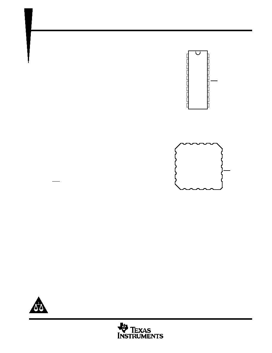
DW OR N PACKAGE
(TOP VIEW)
19
20
1
3
2
17
18
16
15
14
13
12
11
9
10
5
4
6
7
8
V
DD
A0
A1
WR
DB0
REF
AGND
DGND
DB7
DB6
V
OUT
A
OUTB
OUTC
OUTD
DB4
DB3
DB2
DB1
DB5
FK PACKAGE
(TOP VIEW)
SS
LinBiCMOS is a trademark of Texas Instruments.

TLC7226C, TLC7226I, TLC7226M
QUADRUPLE 8 BIT DIGITAL TO ANALOG CONVERTERS
SLAS060E ≠ JANUARY 1995 ≠ REVISED JANUARY 2003
2
POST OFFICE BOX 655303
∑
DALLAS, TEXAS 75265
description (continued)
The TLC7226C is characterized for operation from 0
∞
C to 70
∞
C. The TLC7226I is characterized for operation
from ≠25
∞
C to 85
∞
C. The TLC7226M is characterized for operation from ≠55
∞
C to 125
∞
C.
AVAILABLE OPTIONS
PACKAGE
TA
SMALL OUTLINE
(DW)
PLASTIC DIP
(N)
LCCC
(FK)
0
∞
C to 70
∞
C
TLC7226CDW
TLC7226CN
--
≠25
∞
C to 85
∞
C
TLC7226IDW
TLC7226IN
--
≠55
∞
C to 125
∞
C
--
--
TLC7226MFKB
functional block diagram
_
+
DAC A
Latch
A
8
_
+
DAC B
Latch
B
8
_
+
DAC C
Latch
C
8
_
+
DAC D
Latch
D
8
Control
Logic
8
4
7≠14
15
17
16
REF
DB0≠DB7
WR
A0
A1
2
1
20
19
OUTA
OUTB
OUTC
OUTD
8
8
8
8
schematic of outputs
Output
450
µ
A
VDD
VSS
EQUIVALENT ANALOG OUTPUT

TLC7226C, TLC7226I, TLC7226M
QUADRUPLE 8 BIT DIGITAL TO ANALOG CONVERTERS
SLAS060E ≠ JANUARY 1995 ≠ REVISED JANUARY 2003
3
POST OFFICE BOX 655303
∑
DALLAS, TEXAS 75265
Terminal Functions
TERMINAL
I/O
DESCRIPTION
NAME
NO.
I/O
DESCRIPTION
AGND
5
Analog ground. AGND is the reference and return terminal for the analog signals and supply.
A0, A1
17, 16
I
DAC select inputs. The combination of high or low levels select either DACA, DACB, DACC, or DACD.
DGND
6
Digital ground. DGND is the reference and return terminal for the digital signals and supply.
DB0≠DB7
14≠7
I
Digital DAC data inputs. DB0≠DB7 are the input digital data used for conversion.
OUTA
2
O
DACA output. OUTA is the analog output of DACA.
OUTB
1
O
DACB output. OUTB is the analog output of DACB.
OUTC
20
O
DACC output. OUTC is the analog output of DACC.
OUTD
19
O
DACD output. OUTD is the analog output of DACD.
REF
4
I
Voltage reference input. The voltage level on REF determines the full scale analog output.
VDD
18
Positive supply voltage input terminal
VSS
3
Negative supply voltage input terminal
WR
15
I
Write input. WR selects DAC transparency or latch mode. The selected input latch is transparent when WR
is low.
Terminal numbers shown are for the DW, N, and FK packages.
absolute maximum ratings over operating free-air temperature range (unless otherwise noted)
Supply voltage range, V
DD
: AGND or DGND
≠0.3 V to 17 V
. . . . . . . . . . . . . . . . . . . . . . . . . . . . . . . . . . . . . . . . .
V
SS
≠0.3 V to 24 V
. . . . . . . . . . . . . . . . . . . . . . . . . . . . . . . . . . . . . . . . . . . . . . . . . . .
Supply voltage range, V
SS
: AGND or DGND
≠7 V to 0.3 V
. . . . . . . . . . . . . . . . . . . . . . . . . . . . . . . . . . . . . . . . . .
Voltage range between AGND and DGND
≠17 V to 17 V
. . . . . . . . . . . . . . . . . . . . . . . . . . . . . . . . . . . . . . . . . . . .
Input voltage range, V
I
(to DGND)
≠0.3 V to V
DD
+ 0.3 V
. . . . . . . . . . . . . . . . . . . . . . . . . . . . . . . . . . . . . . . . . . . .
Reference voltage range: V
ref
(to AGND)
≠0.3 V to V
DD
. . . . . . . . . . . . . . . . . . . . . . . . . . . . . . . . . . . . . . . . . . .
V
ref
(to V
SS
)
≠0.3 V to 20 V
. . . . . . . . . . . . . . . . . . . . . . . . . . . . . . . . . . . . . . . . . . . . .
Output voltage range, V
O
(to AGND) (see Note 1)
V
SS
to V
DD
. . . . . . . . . . . . . . . . . . . . . . . . . . . . . . . . . . . . . . . .
Continuous total power dissipation at (or below) T
A
= 25
∞
C (see Note 2)
500 mW
. . . . . . . . . . . . . . . . . . . . . . .
Operating free-air temperature range, T
A
: C suffix
0
∞
C to 70
∞
C
. . . . . . . . . . . . . . . . . . . . . . . . . . . . . . . . . . . . . . .
E suffix
≠25
∞
C to 85
∞
C
. . . . . . . . . . . . . . . . . . . . . . . . . . . . . . . . . . . . .
M suffix
≠55
∞
C to 125
∞
C
. . . . . . . . . . . . . . . . . . . . . . . . . . . . . . . . . . . .
Storage temperature range, T
stg
≠65
∞
C to 150
∞
C
. . . . . . . . . . . . . . . . . . . . . . . . . . . . . . . . . . . . . . . . . . . . . . . . . . .
Lead temperature 1,6 mm (1/16 inch) from case for 10 seconds: DW or N packages
260
∞
C
. . . . . . . . . . . . . .
Case temperature for 10 seconds: FK package
260
∞
C
. . . . . . . . . . . . . . . . . . . . . . . . . . . . . . . . . . . . . . . . . . . . . .
Stresses beyond those listed under "absolute maximum ratings" may cause permanent damage to the device. These are stress ratings only, and
functional operation of the device at these or any other conditions beyond those indicated under "recommended operating conditions" is not
implied. Exposure to absolute-maximum-rated conditions for extended periods may affect device reliability.
The VSS terminal is connected to the substrate and must be tied to the most negative supply voltage applied to the device.
NOTES:
1. Output voltages may be shorted to AGND provided that the power dissipation of the package is not exceeded. Typically short circuit
current to AGND is 60 mA.
2. For operation above TA = 75
∞
C, derate linearly at the rate of 2 mW/
∞
C.

TLC7226C, TLC7226I, TLC7226M
QUADRUPLE 8 BIT DIGITAL TO ANALOG CONVERTERS
SLAS060E ≠ JANUARY 1995 ≠ REVISED JANUARY 2003
4
POST OFFICE BOX 655303
∑
DALLAS, TEXAS 75265
recommended operating conditions
MIN
MAX
UNIT
Supply voltage, VDD
11.4
16.5
V
Supply voltage, VSS
≠5.5
0
V
High-level input voltage, VIH
2
V
Low-level input voltage, VIL
0.8
V
Reference voltage, Vref
0
VDD≠4
V
Load resistance, RL
2
k
Setup time, address valid before WR
, tsu(AW) (see Figure 6)
VDD = 11.4 V to 16.5 V
*0
ns
Setup time, data valid before WR
, tsu(DW) (see Figure 6)
VDD = 11.4 V to 16.5 V
*45
ns
Hold time, address valid before WR
, th(AW) (see Figure 6)
VDD = 11.4 V to 16.5 V
*0
ns
Hold time, data valid before WR
, th(DW) (see Figure 6)
VDD = 11.4 V to 16.5 V
*10
ns
Pulse duration, WR low, tw (see Figure 6)
VDD = 11.4 V to 16.5 V
*50
ns
C suffix
0
70
Operating free-air temperature, TA
I suffix
≠25
85
∞
C
O erating free air tem erature, TA
M suffix
≠55
125
C
* This parameter is not tested for M suffix devices.
electrical characteristics over recommended operating free-air temperature range
dual power supply over recommended power supply and reference voltage ranges, AGND = DGND = 0 V
(unless otherwise noted)
PARAMETER
TEST CONDITIONS
MIN
TYP
MAX
UNIT
II
Input current, digital
VI = 0 V or VDD
±
1
µ
A
I(DD)
Supply current
VI = 0.8 V or 2.4 V,
VSS = ≠ 5 V,
VDD = 16.5 V,
No load
6
16
mA
I(SS)
Supply current
VI = 0.8 V or 2.4 V, No load
4
10
mA
ri(ref)
Reference input resistance
2
4
k
Power supply sensitivity
VDD =
±
5%
0.01
%/%
All 0s loaded
C and I suffix
65
REF input
All 0s loaded
M suffix
*30
Ci
Input capacitance
REF in ut
All 1s loaded
*300
pF
Ci
In ut ca acitance
Digital inputs
C and I suffix
8
F
Digital inputs
M suffix
*12
* This parameter is not tested for M suffix devices.

TLC7226C, TLC7226I, TLC7226M
QUADRUPLE 8 BIT DIGITAL TO ANALOG CONVERTERS
SLAS060E ≠ JANUARY 1995 ≠ REVISED JANUARY 2003
5
POST OFFICE BOX 655303
∑
DALLAS, TEXAS 75265
operating characteristics over recommended operating free-air temperature range
dual power supply over recommended power supply and reference voltage ranges, AGND = DGND = 0 V
(unless otherwise noted)
PARAMETER
TEST CONDITIONS
MIN
TYP
MAX
UNIT
Slew rate
*2.5
V
∑µ
s
Settling time to 1/2 LSB
Positive full scale
V
10 V
*5
s
Settling time to 1/2 LSB
Negative full scale
Vref = 10 V
*7
µ
s
Resolution
8
bits
Total unadjusted error
±
2
LSB
Linearity error
Differential/integral
V
15 V
±
5%
V
10 V
±
1
LSB
Full-scale error
VDD = 15 V
±
5%,
Vref = 10 V
±
2
LSB
Gain error
±
0.25
LSB
Temperat re coefficient of gain
Full scale
VDD = 14 V to 16.5 V, Vref = 10 V
±
20
ppm/
∞
C
Temperature coefficient of gain
Zero-code error
±
50
µ
V/
∞
C
Zero-code error
±
20
±
80
mV
Digital crosstalk glitch impulse area
Vref = 0
50
nV
∑
s
* This parameter is not tested for M suffix devices.
single power supply, V
DD
= 14.25 V to 15.75 V, V
SS
= AGND = DGND = 0 V, V
ref
= 10 V (unless otherwise noted)
PARAMETER
TEST CONDITIONS
MIN
TYP
MAX
UNIT
Supply current, IDD
VI = 0.8 V or 2.4 V,
No load
5
13
mA
Slew rate
*2
V
∑µ
s
Settling time to 1/2 LSB
Positive full scale
*5
s
Settling time to 1/2 LSB
Negative full scale
*20
µ
s
Resolution
8
bits
Total unadjusted error
±
2
LSB
Full-scale error
±
2
LSB
Temperature coefficient of gain
Full scale
VDD = 14 V to 16.5 V, Vref = 10 V
±
20
ppm/
∞
C
Temperature coefficient of gain
Zero-code error
±
50
µ
V/
∞
C
Linearity error
Differential
±
1
LSB
Digital crosstalk-glitch impulse area
50
nV
∑
s
* This parameter is not tested for M suffix devices.