 | –≠–ª–µ–∫—Ç—Ä–æ–Ω–Ω—ã–π –∫–æ–º–ø–æ–Ω–µ–Ω—Ç: TLE2061BC | –°–∫–∞—á–∞—Ç—å:  PDF PDF  ZIP ZIP |
TLE206x, TLE206xA, TLE206xB, TLE206xY
EXCALIBUR JFET-INPUT HIGH-OUTPUT-DRIVE
µ
POWER OPERATIONAL AMPLIFIERS
SLOS193A ≠ FEBRUARY 1997 ≠ REVISED MARCH 1998
1
POST OFFICE BOX 655303
∑
DALLAS, TEXAS 75265
D
2
◊
Bandwidth (2 MHz) of the TL06x and
TL03x Operational Amplifiers
D
Low Supply Current . . . 290
µ
A/Ch Typ
D
On-chip Offset Voltage Trimming for
Improved DC Performance
D
High Output Drive, Specified into 100-
Loads
D
Lower Noise Floor Than Earlier
Generations of Low-Power BiFETs
description
The TLE206x series of low-power JFET-input operational amplifiers doubles the bandwidth of the earlier
generation TL06x and TL03x BiFET families without significantly increasing power consumption. Texas
Instruments Excalibur process also delivers a lower noise floor than the TL06x and TL03x. On-chip zener
trimming of offset voltage yields precision grades for dc-coupled applications. The TL206x devices are
pin-compatible with other TI BiFETs; they can be used to double the bandwidth of TL06x and TL03x circuits,
or to reduce power consumption of TL05x, TL07x, and TL08x circuits by nearly 90%.
BiFET operational amplifiers offer the inherently-higher input impedance of the JFET-input transistors, without
sacrificing the output drive associated with bipolar amplifiers. This makes them better suited for interfacing with
high-impedance sensors or very low-level ac signals. They also feature inherently better ac response than
bipolar or CMOS devices having comparable power consumption. The TLE206x family features a
high-output-drive circuit capable of driving 100-
loads at supplies as low as
±
5 V. This makes them uniquely
suited for driving transformer loads in modems and other applications requiring good ac characteristics, low
power, and high output drive.
Because BiFET operational amplifiers are designed for use with dual power supplies, care must be taken to
observe common-mode input voltage limits and output swing when operating from a single supply. DC biasing
of the input signal is required and loads should be terminated to a virtual ground node at mid-supply. Texas
Instruments TLE2426 integrated virtual ground generator is useful when operating BiFET amplifiers from single
supplies.
The TLE206x are fully specified at
±
15 V and
±
5 V. For operation in low-voltage and/or single-supply systems,
Texas Instruments LinCMOS families of operational amplifiers (TLC- and TLV-prefixes) are recommended.
When moving from BiFET to CMOS amplifiers, particular attention should be paid to slew rate and bandwidth
requirements, and output loading. The Texas Instrument TLV2432 and TLV2442 CMOS operational amplifiers
are excellent choices to consider.
Copyright
©
1998, Texas Instruments Incorporated
PRODUCTION DATA information is current as of publication date.
Products conform to specifications per the terms of Texas Instruments
standard warranty. Production processing does not necessarily include
testing of all parameters.
Please be aware that an important notice concerning availability, standard warranty, and use in critical applications of
Texas Instruments semiconductor products and disclaimers thereto appears at the end of this data sheet.
TLE206x, TLE206xA, TLE206xB, TLE206xY
EXCALIBUR JFET-INPUT HIGH-OUTPUT-DRIVE
µ
POWER OPERATIONAL AMPLIFIERS
SLOS193A ≠ FEBRUARY 1997 ≠ REVISED MARCH 1998
2
POST OFFICE BOX 655303
∑
DALLAS, TEXAS 75265
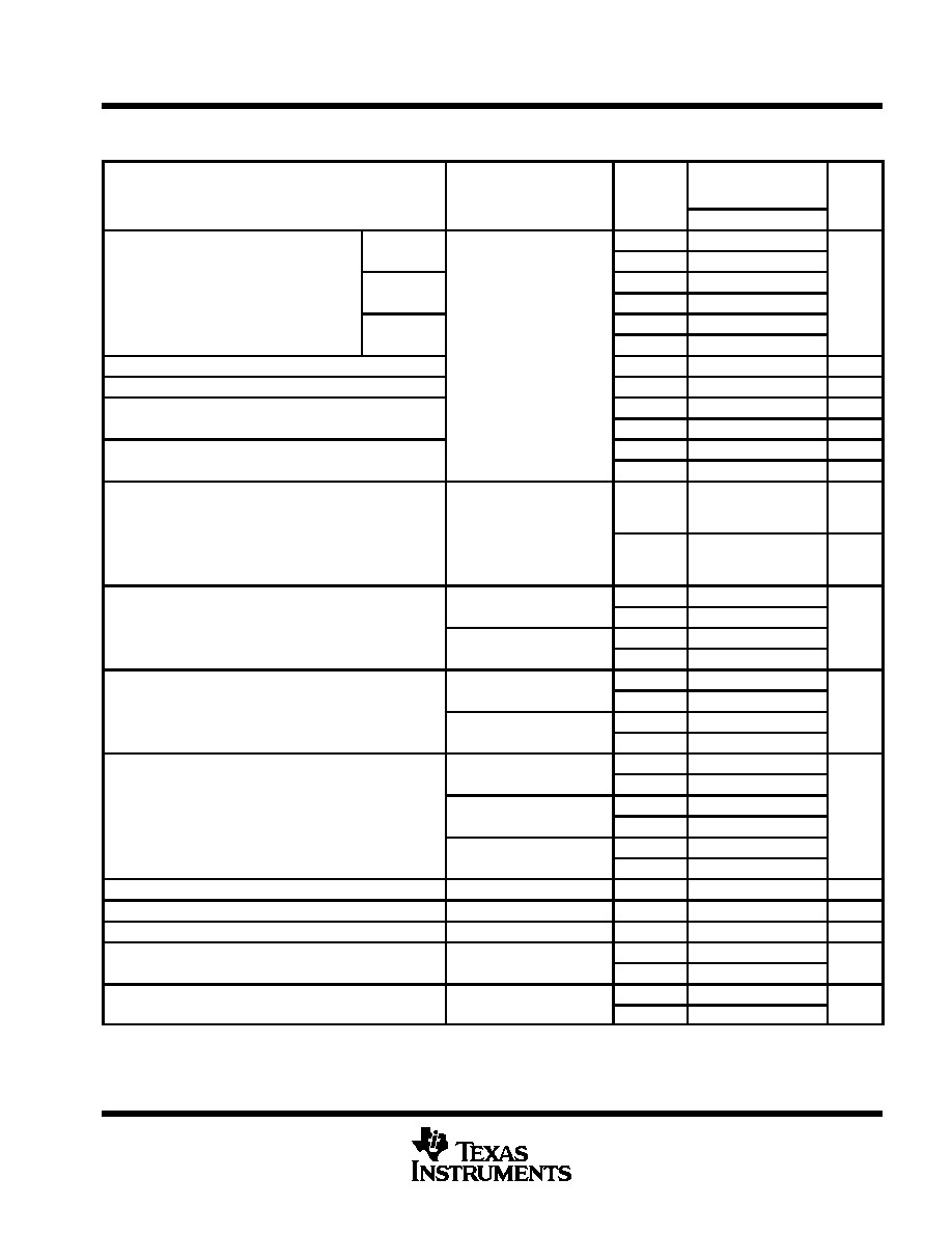
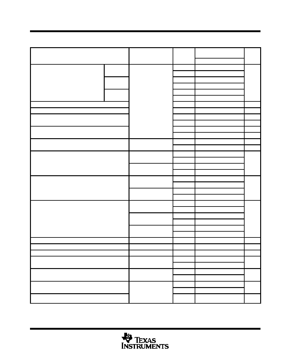
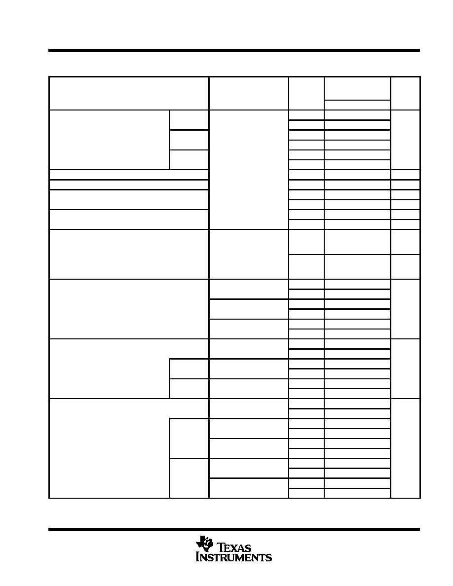
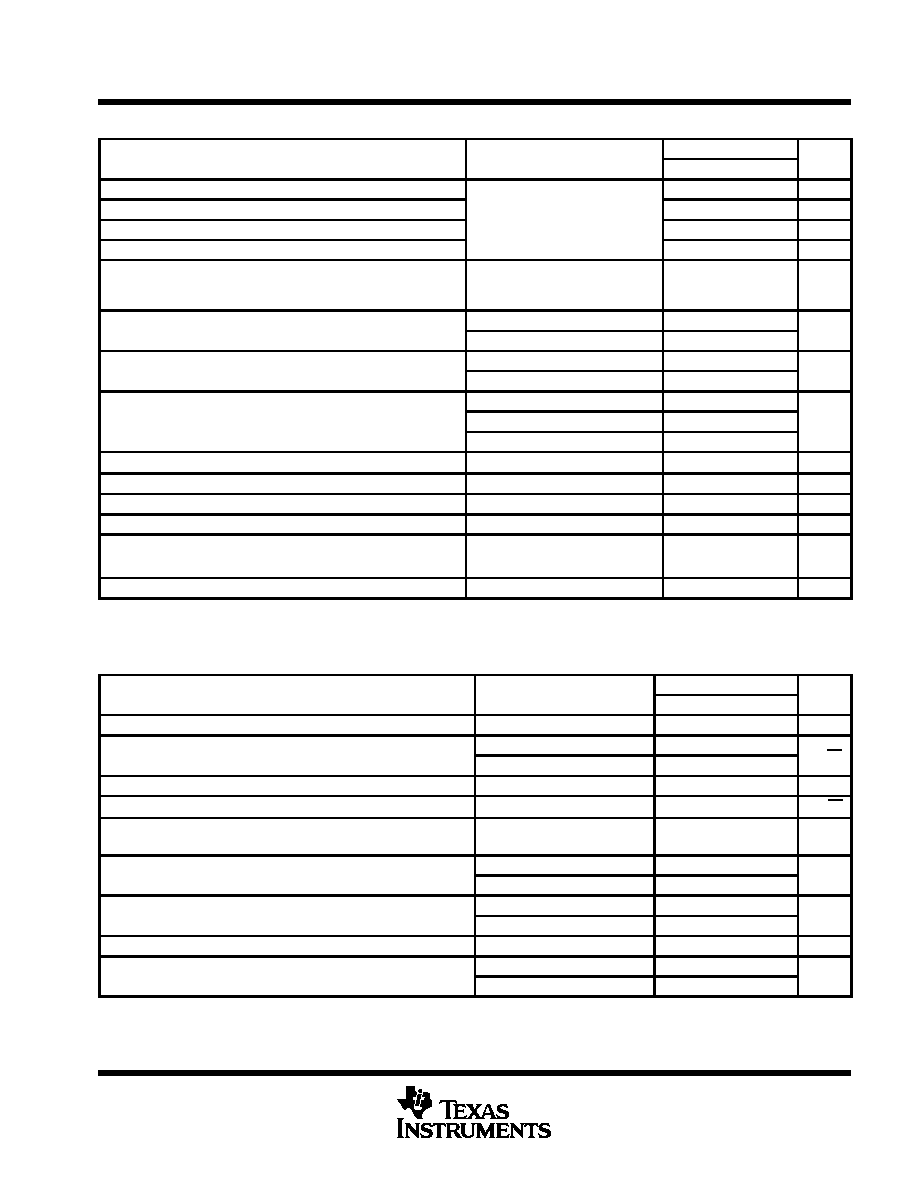
TLE2061 AVAILABLE OPTIONS
PACKAGED DEVICES
CHIP
TA
VIOmax
AT 25
∞
C
SMALL
OUTLINE
(D)
CHIP
CARRIER
(FK)
CERAMIC
DIP
(JG)
PLASTIC
DIP
(P)
TSSOP
(PW)
CHIP
FORMß
(Y)
500
µ
V
--
--
--
--
--
--
0
∞
C to 70
∞
C
1.5 mV
TLE2061ACD
--
--
TLE2061ACP
--
--
3 mV
TLE2061CD
--
--
TLE2061CP
TLE2061CPWLE
TLE2061Y
500
µ
V
--
--
--
--
--
--
≠ 40
∞
C to 85
∞
C
1.5 mV
TLE2061AID
--
--
TLE2061AIP
--
--
3 mV
TLE2061ID
--
--
TLE2061IP
--
--
500
µ
V
--
--
TLE2061BMJG
--
--
--
≠ 55
∞
C to 125
∞
C
1.5 mV
TLE2061AMD
TLE2061AMFK
TLE2061AMJG
TLE2061AMP
--
--
3 mV
TLE2061MD
TLE2061MFK
TLE2061MJG
TLE2061MP
--
--
The D packages are available taped and reeled. Add R suffix to device type (e.g., TLE2061ACDR).Chips are tested at 25
∞
C.
The PW package is available left-end taped and reeled (indicated by the LE suffix on the device type (e.g., TLE2061CPWLE).
ß Chip forms are tested at 25
∞
C only.
TLE2062 AVAILABLE OPTIONS
PACKAGED DEVICES
CHIP FORM
TA
VIOmax
AT 25
∞
C
SMALL OUTLINE
(D)
CHIP CARRIER
(FK)
CERAMIC DIP
(JG)
PLASTIC DIP
(P)
CHIP FORM
(Y)
0
∞
C
to
70
∞
C
1 mV
2 mV
4 mV
TLE2062BCD
TLE2062ACD
TLE2062CD
--
--
--
--
--
--
TLE2062BCP
TLE2062ACP
TLE2062CP
--
--
TLE2062Y
≠ 40
∞
C
to
85
∞
C
1 mV
2 mV
4 mV
TLE2062BID
TLE2062AID
TLE2062ID
--
--
--
--
--
--
TLE2062BIP
TLE2062AIP
TLE2062IP
--
--
--
≠ 55
∞
C
to
125
∞
C
1 mV
2 mV
4 mV
TLE2062BMD
TLE2062AMD
TLE2062MD
TLE2062BMFK
TLE2062AMFK
TLE2062MFK
TLE2062BMJG
TLE2062AMJG
TLE2062MJG
TLE2062BMP
TLE2062AMP
TLE2062MP
--
--
--
The D packages are available taped and reeled. Add R suffix to device type (e.g., TLE2062ACDR).
Chip forms are tested at 25
∞
C only.
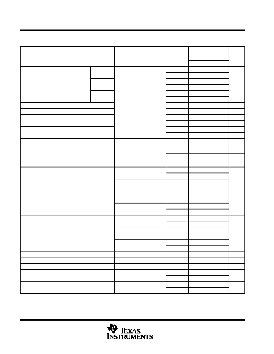
TLE2064 AVAILABLE OPTIONS
PACKAGED DEVICES
CHIP FORM
VIOmax
SMALL OUTLINE
CHIP CARRIER
CERAMIC DIP
PLASTIC DIP
CHIP FORM
TA
VIOmax
AT 25
∞
C
SMALL OUTLINE
(D)
CHIP CARRIER
(FK)
CERAMIC DIP
(J)
PLASTIC DIP
(N)
(Y)
TA
AT 25
∞
C
(D)
(FK)
(J)
(N)
( )
0
∞
C
to
70
∞
C
2 mV
4 mV
6 mV
--
TLE2064ACD
TLE2064CD
--
--
TLE2064BCN
TLE2064ACN
TLE2064CN
--
--
TLE2064Y
≠ 40
∞
C
to
85
∞
C
2 mV
4 mV
6 mV
--
TLE2064AID
TLE2064ID
--
--
TLE2064BIN
TLE2064AIN
TLE2064IN
--
--
--
≠ 55
∞
C
to
125
∞
C
2 mV
4 mV
6 mV
--
TLE2064AMD
TLE2064MD
--
TLE2064AMFK
TLE2064MFK
TLE2064BMJ
TLE2064AMJ
TLE2064MJ
TLE2064BMN
TLE2064AMN
TLE2064MN
--
--
--
The D packages are available taped and reeled. Add R suffix to device type, (e.g., TLE2064ACDR).
Chip forms are tested at 25
∞
C only.
TLE206x, TLE206xA, TLE206xB, TLE206xY
EXCALIBUR JFET-INPUT HIGH-OUTPUT-DRIVE
µ
POWER OPERATIONAL AMPLIFIERS
SLOS193A ≠ FEBRUARY 1997 ≠ REVISED MARCH 1998
3
POST OFFICE BOX 655303
∑
DALLAS, TEXAS 75265
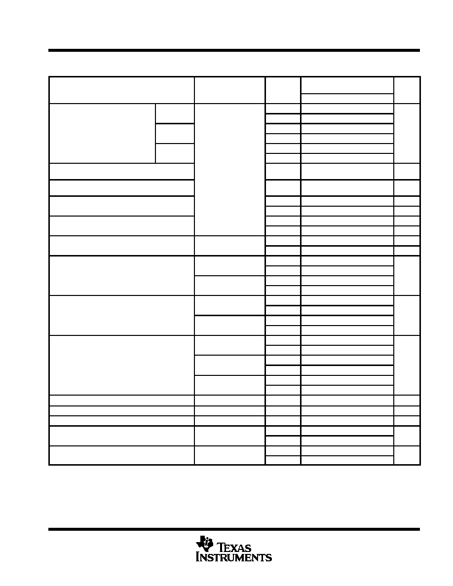
1
2
3
4
8
7
6
5
OFFSET N1
IN ≠
IN +
V
CC ≠
NC
V
CC +
OUT
OFFSET N2
NC ≠ No internal connection
3
2
1 20 19
9 10 11 12 13
4
5
6
7
8
18
17
16
15
14
NC
V
CC +
NC
OUT
NC
NC
IN ≠
NC
IN +
NC
NC
OFFSET
N1
NC
NC
NC
NC
NC
OFFSET
N2
NC
CC
≠
V
TLE2061, TLE2061A, AND TLE2061B
D, DB, JG, P, OR PW PACKAGE
(TOP VIEW)
TLE2061M, TLE2061AM, TLE2061BM
FK PACKAGE
(TOP VIEW)
1
2
3
4
8
7
6
5
1OUT
1IN ≠
1IN +
V
CC ≠
V
CC +
2OUT
2IN ≠
2IN +
3
2
1 20 19
9 10 11 12 13
4
5
6
7
8
18
17
16
15
14
NC
2OUT
NC
2IN ≠
NC
NC
1IN ≠
NC
1IN+
NC
NC
NC
NC
NC
NC
V
NC
2IN+
CC ≠
V
CC +
1OUT
TLE2062, TLE2062A, TLE2062B
D, JG, OR P PACKAGE
(TOP VIEW)
TLE2062M, TLE2062AM, TLE2062BM
FK PACKAGE
(TOP VIEW)
4OUT
3
2
1 20 19
9 10 11 12 13
4
5
6
7
8
18
17
16
15
14
4IN +
NC
V
CC ≠
NC
3IN +
1IN +
NC
V
CC +
NC
2IN +
1IN ≠
1OUT
NC
3IN ≠
4IN ≠
2IN ≠
NC
3OUT
1
2
3
4
5
6
7
14
13
12
11
10
9
8
1OUT
1IN ≠
1IN +
V
CC +
2IN +
2IN ≠
2OUT
4OUT
4IN ≠
4IN +
V
CC ≠
3IN +
3IN ≠
3OUT
2OUT
TLE2064, TLE2064A, TLE2064B
D, J, OR N PACKAGE
(TOP VIEW)
TLE2064M, TLE2064AM, TLE2064BM
FK PACKAGE
(TOP VIEW)
TLE206x, TLE206xA, TLE206xB, TLE206xY
EXCALIBUR JFET-INPUT HIGH-OUTPUT-DRIVE
µ
POWER OPERATIONAL AMPLIFIERS
SLOS193A ≠ FEBRUARY 1997 ≠ REVISED MARCH 1998
4
POST OFFICE BOX 655303
∑
DALLAS, TEXAS 75265
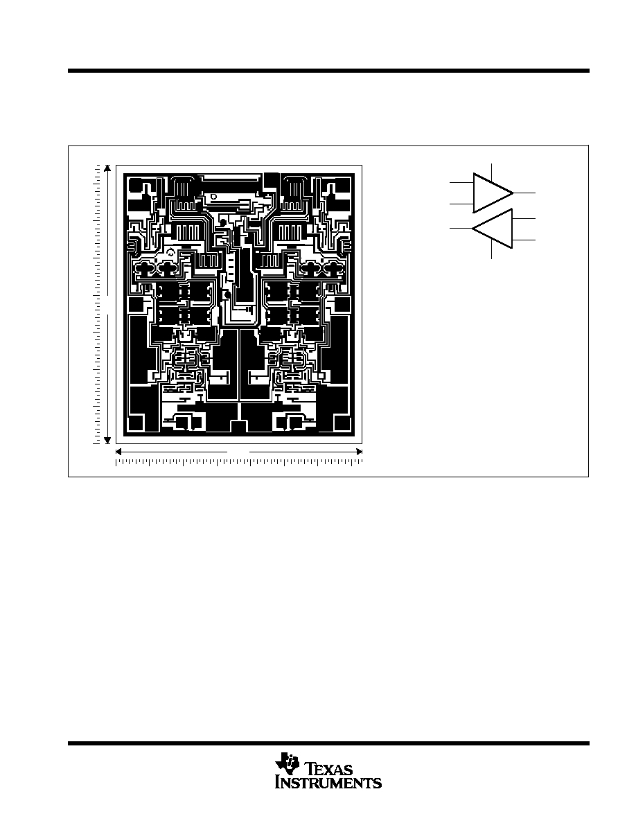
TLE2061Y chip information
This chip, when properly assembled, displays characteristics similar to the TLE2061. Thermal compression or
ultrasonic bonding may be used on the doped-aluminum bonding pads. Chips may be mounted with conductive
epoxy or a gold-silicon preform.
OFFSET N1
IN +
IN ≠
OFFSET N2
VCC +
VCC ≠
OUT
CHIP THICKNESS: 15 MILS TYPICAL
BONDING PADS: 4 X 4 MILS MINIMUM
TJmax = 150
∞
C
TOLERANCES ARE
±
10%.
ALL DIMENSIONS ARE IN MILS.
PIN (4) IS INTERNALLY CONNECTED
TO BACKSIDE OF CHIP.
BONDING PAD ASSIGNMENTS
(7)
(6)
(4)
(1)
(3)
(2)
(5)
45
65
(7)
(6)
(1)
(3)
(2)
(5)
(4)
TLE206x, TLE206xA, TLE206xB, TLE206xY
EXCALIBUR JFET-INPUT HIGH-OUTPUT-DRIVE
µ
POWER OPERATIONAL AMPLIFIERS
SLOS193A ≠ FEBRUARY 1997 ≠ REVISED MARCH 1998
5
POST OFFICE BOX 655303
∑
DALLAS, TEXAS 75265
TLE2062Y chip information
This chip, when properly assembled, displays characteristics similar to the TLE2062. Thermal compression or
ultrasonic bonding may be used on the doped-aluminum bonding pads. Chips may be mounted with conductive
epoxy or a gold-silicon preform.
BONDING PAD ASSIGNMENTS
CHIP THICKNESS: 15 MILS TYPICAL
BONDING PADS: 4
◊
4 MILS MINIMUM
TJmax = 150
∞
C
TOLERANCES ARE
±
10%.
ALL DIMENSIONS ARE IN MILS.
PIN (4) IS INTERNALLY CONNECTED
TO BACKSIDE OF THE CHIP.
+
≠
1OUT
1IN +
1IN ≠
VCC+
(4)
(6)
(3)
(2)
(5)
(1)
(7)
(8)
≠
+
2OUT
2IN +
2IN ≠
VCC ≠
73
75
(1)
(2)
(3)
(4)
(5)
(6)
(7)
(8)
TLE206x, TLE206xA, TLE206xB, TLE206xY
EXCALIBUR JFET-INPUT HIGH-OUTPUT-DRIVE
µ
POWER OPERATIONAL AMPLIFIERS
SLOS193A ≠ FEBRUARY 1997 ≠ REVISED MARCH 1998
6
POST OFFICE BOX 655303
∑
DALLAS, TEXAS 75265
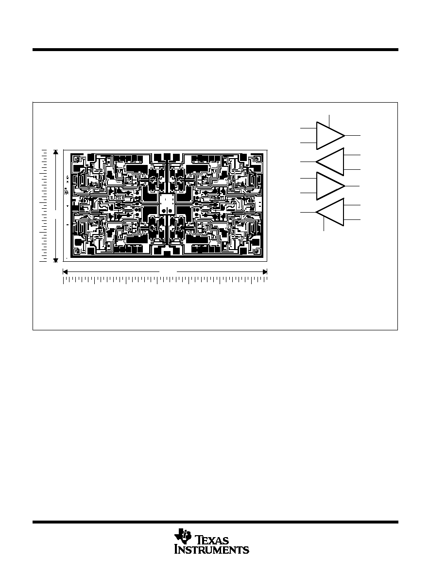
TLE2064Y chip information
This chip, when properly assembled, displays characteristics similar to the TLE2064. Thermal compression or
ultrasonic bonding may be used on the doped-aluminum bonding pads. Chips may be mounted with conductive
epoxy or a gold-silicon preform.
BONDING PAD ASSIGNMENTS
CHIP THICKNESS: 15 MILS TYPICAL
BONDING PADS: 4
◊
4 MILS MINIMUM
TJmax = 150
∞
C
TOLERANCES ARE
±
10%.
ALL DIMENSIONS ARE IN MILS.
PIN (11) IS INTERNALLY CONNECTED
TO BACKSIDE OF CHIP.
+
≠
1 OUT
1 IN +
1 IN ≠
VCC+
(4)
(6)
(3)
(2)
(5)
(1)
≠
+
(7)
2 IN +
2 IN ≠
2 OUT
(11)
+
≠
3 OUT
3 IN +
3 IN ≠
(13)
(10)
(9)
(12)
(8)
≠
+
(14)
4 OUT
4 IN +
4 IN ≠
VCC ≠
139
73
(1)
(2)
(4)
(7)
(5)
(6)
(8)
(11)
(9)
(10)
(12)
(13)
(14)
(3)
TLE206x, TLE206xA, TLE206xB, TLE206xY
EXCALIBUR JFET
-INPUT HIGH-OUTPUT
-DRIVE
POWER OPERA
TIONAL
AMPLIFIERS
SLOS193A
≠ FEBRUAR
Y
1997 ≠ REVISED MARCH 1998
µ
POST
OFFICE BOX 655303 DALLAS,
TEXAS
75265
∑
6≠7
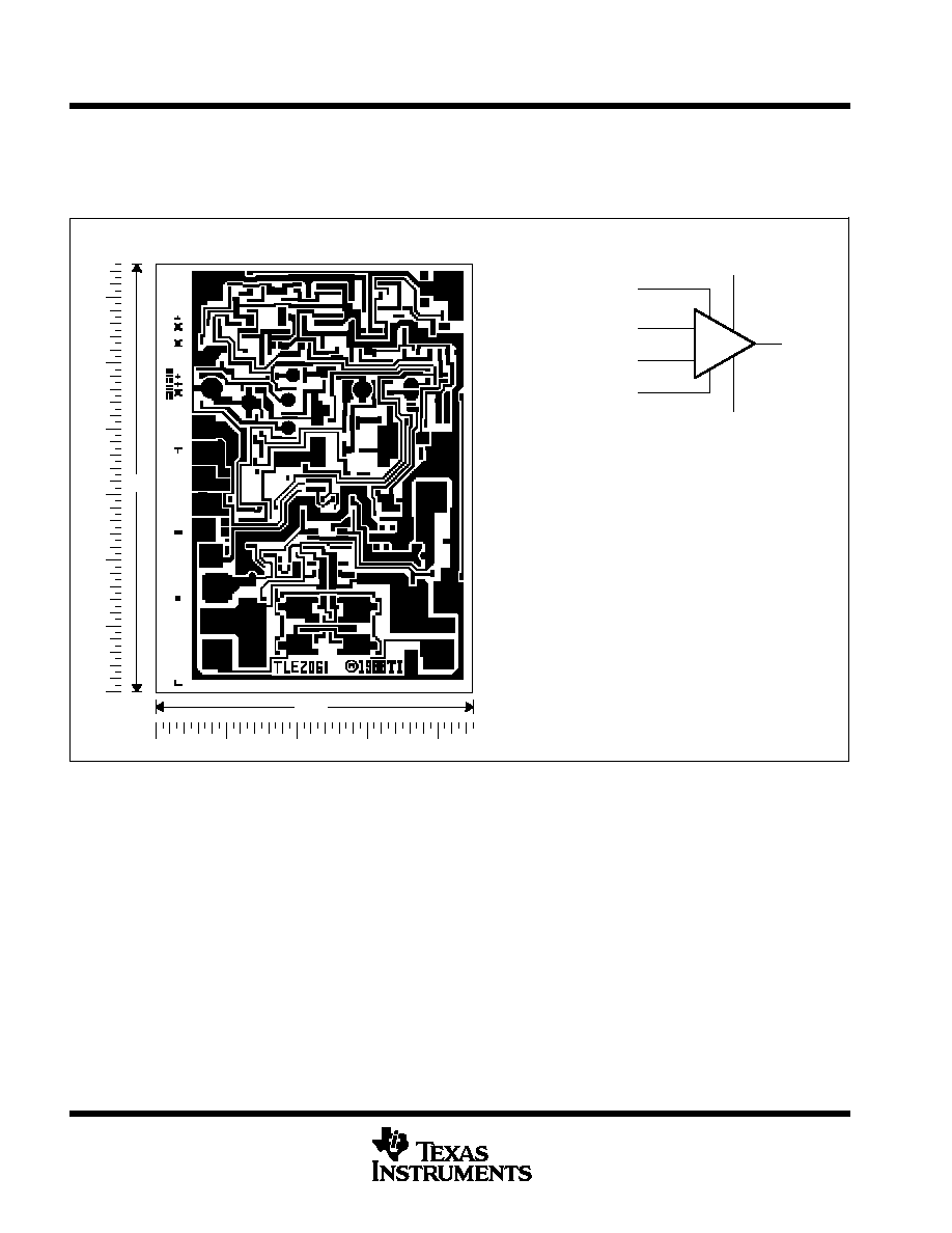
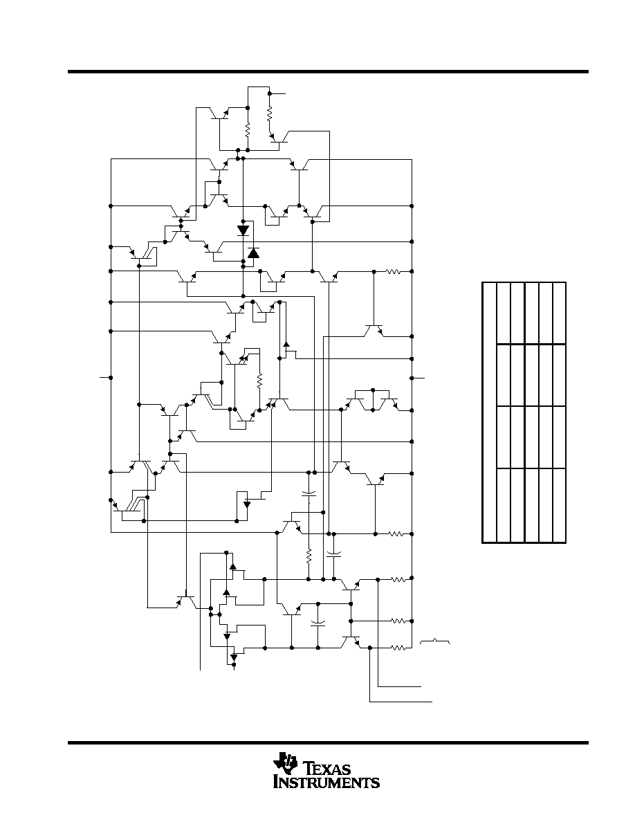
equivalent schematic (each channel)
Q20
VCC ≠
VCC +
Q13
Q9
Q14
Q16
Q4
IN +
IN ≠
Q1
Q5
Q7
Q3
Q6
C1
Q2
Q12
Q15
Q21
Q22
Q26
Q31
Q10
Q11
Q18
Q19
Q25
Q27
Q17
Q23
Q28
Q24
D1
Q30
Q29
Q32
Q35
Q33
Q34
Q36
D2
Q37
Q38
Q40
Q41
Q42
Q39
OUT
R1
1.1 k
R4
55 k
R2
1.1 k
Q8
15 pF
R6
2.7 k
R8
20
R9
100
R7
600
R5
60 k
R3
2.4 k
C3
5.3 pF
C2
15 pF
See Note A
OFFSET N2
OFFSET N1
NOTES: A. OFFSET N1 AND OFFSET N2 are only availiable on the TLE2061x devices.
B. Component values are nominal.
ACTUAL DEVICE COMPONENT COUNT
COMPONENT
TLE2061
TLE2062
TLE2064
Transistors
43
42
42
Resistors
9
9
9
Diodes
1
2
2
Capacitors
3
3
3
TLE206x, TLE206xA, TLE206xB, TLE206xY
EXCALIBUR JFET-INPUT HIGH-OUTPUT-DRIVE
µ
POWER OPERATIONAL AMPLIFIERS
SLOS193A ≠ FEBRUARY 1997 ≠ REVISED MARCH 1998
8
POST OFFICE BOX 655303
∑
DALLAS, TEXAS 75265
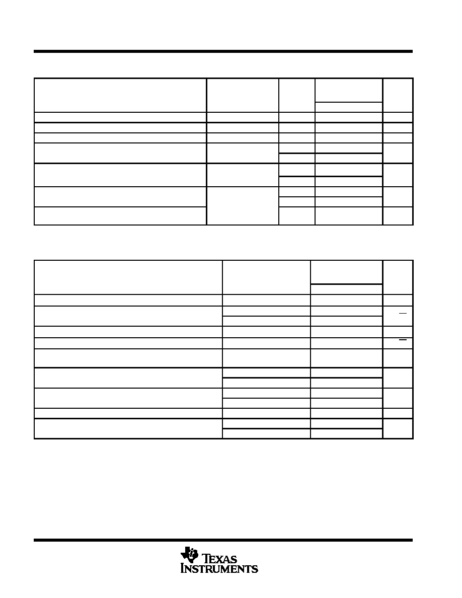
absolute maximum ratings over operating free-air temperature range (unless otherwise noted)
Supply voltage, V
CC+
(see Note 1)
19 V
. . . . . . . . . . . . . . . . . . . . . . . . . . . . . . . . . . . . . . . . . . . . . . . . . . . . . . . . . . .
Supply voltage, V
CC ≠
≠ 19 V
. . . . . . . . . . . . . . . . . . . . . . . . . . . . . . . . . . . . . . . . . . . . . . . . . . . . . . . . . . . . . . . . . . . . .
Differential input voltage, V
ID
(see Note 2)
±
38 V
. . . . . . . . . . . . . . . . . . . . . . . . . . . . . . . . . . . . . . . . . . . . . . . . . . .
Input voltage range, V
I
(any input)
±
V
CC
. . . . . . . . . . . . . . . . . . . . . . . . . . . . . . . . . . . . . . . . . . . . . . . . . . . . . . . . . . .
Input current, I
I
(each input)
±
1 mA
. . . . . . . . . . . . . . . . . . . . . . . . . . . . . . . . . . . . . . . . . . . . . . . . . . . . . . . . . . . . . . .
Output current, I
O
±
80 mA
. . . . . . . . . . . . . . . . . . . . . . . . . . . . . . . . . . . . . . . . . . . . . . . . . . . . . . . . . . . . . . . . . . . . . . .
Total current into V
CC+
80 mA
. . . . . . . . . . . . . . . . . . . . . . . . . . . . . . . . . . . . . . . . . . . . . . . . . . . . . . . . . . . . . . . . . . .
Total current out of V
CC ≠
≠ 80 mA
. . . . . . . . . . . . . . . . . . . . . . . . . . . . . . . . . . . . . . . . . . . . . . . . . . . . . . . . . . . . . . . .
Duration of short-circuit current at (or below) 25
∞
C (see Note 3)
unlimited
. . . . . . . . . . . . . . . . . . . . . . . . . . . . .
Continuous total dissipation
See Dissipation Rating Table
. . . . . . . . . . . . . . . . . . . . . . . . . . . . . . . . . . . . . . . . . . .
Operating free-air temperature range, T
A
: C suffix
0
∞
C to 70
∞
C
. . . . . . . . . . . . . . . . . . . . . . . . . . . . . . . . . . . . . .
I suffix
≠ 40
∞
C to 85
∞
C
. . . . . . . . . . . . . . . . . . . . . . . . . . . . . . . . . . . . .
M suffix
≠ 55
∞
C to 125
∞
C
. . . . . . . . . . . . . . . . . . . . . . . . . . . . . . . . . .
Storage temperature range
≠ 65
∞
C to 150
∞
C
. . . . . . . . . . . . . . . . . . . . . . . . . . . . . . . . . . . . . . . . . . . . . . . . . . . . . . .
Case temperature for 60 seconds: FK package
260
∞
C
. . . . . . . . . . . . . . . . . . . . . . . . . . . . . . . . . . . . . . . . . . . . . .
Lead temperature 1,6 mm (1/16 inch) from case for 10 seconds: D, P, or PW package
260
∞
C
. . . . . . . . . . . .
Lead temperature 1,6 mm (1/16 inch) from case for 60 seconds: JG package
300
∞
C
. . . . . . . . . . . . . . . . . . . .
Stresses beyond those listed under "absolute maximum ratings" may cause permanent damage to the device. These are stress ratings only, and
functional operation of the device at these or any other conditions beyond those indicated under "recommended operating conditions" is not
implied. Exposure to absolute-maximum-rated conditions for extended periods may affect device reliability.
NOTES:
1. All voltage values, except differential voltages, are with respect to the midpoint between VCC+ and VCC ≠ .
2. Differential voltages are at IN+ with respect to IN ≠.
3. The output may be shorted to either supply. Temperature and /or supply voltages must be limited to ensure that the maximum
dissipation rating is not exceeded.
DISSIPATION RATING TABLE
PACKAGE
TA
25
∞
C
POWER RATING
DERATING FACTOR
ABOVE TA = 25
∞
C
TA = 70
∞
C
POWER RATING
TA = 85
∞
C
POWER RATING
TA = 125
∞
C
POWER RATING
D≠8
725 mW
5.8 mW/
∞
C
464 mW
377 mW
145 mW
D≠14
950 mW
7.6 mW/
∞
C
608 mW
494 mW
190 mW
FK
1375 mW
11.0 mW/
∞
C
880 mW
715 mW
275 mW
J
1375 mW
11.0 mW/
∞
C
880 mW
715 mW
275 mW
JG
1050 mW
8.4 mW/
∞
C
672 mW
546 mW
210 mW
N
1150 mW
9.2 mW/
∞
C
736 mW
598 mW
230 mW
P
1000 mW
8.0 mW/
∞
C
640 mW
520 mW
200 mW
PW
525 mW
4.2 mW/
∞
C
336 mW
--
--
recommended operating conditions
C SUFFIX
I SUFFIX
M SUFFIX
UNIT
MIN
MAX
MIN
MAX
MIN
MAX
UNIT
Supply voltage, VCC
±
±
3.5
±
18
±
3.5
±
18
±
3.5
±
18
V
Common mode input voltage VIC
VCC
±
=
±
5 V
≠ 1.6
4
≠ 1.6
4
≠ 1.6
4
V
Common-mode input voltage, VIC
VCC
±
=
±
15 V
≠ 11
13
≠ 11
13
≠ 11
13
V
Operating free-air temperature, TA
0
70
≠ 40
85
≠ 55
125
∞
C
TLE206x, TLE206xA, TLE206xB, TLE206xY
EXCALIBUR JFET-INPUT HIGH-OUTPUT-DRIVE
µ
POWER OPERATIONAL AMPLIFIERS
SLOS193A ≠ FEBRUARY 1997 ≠ REVISED MARCH 1998
9
POST OFFICE BOX 655303
∑
DALLAS, TEXAS 75265
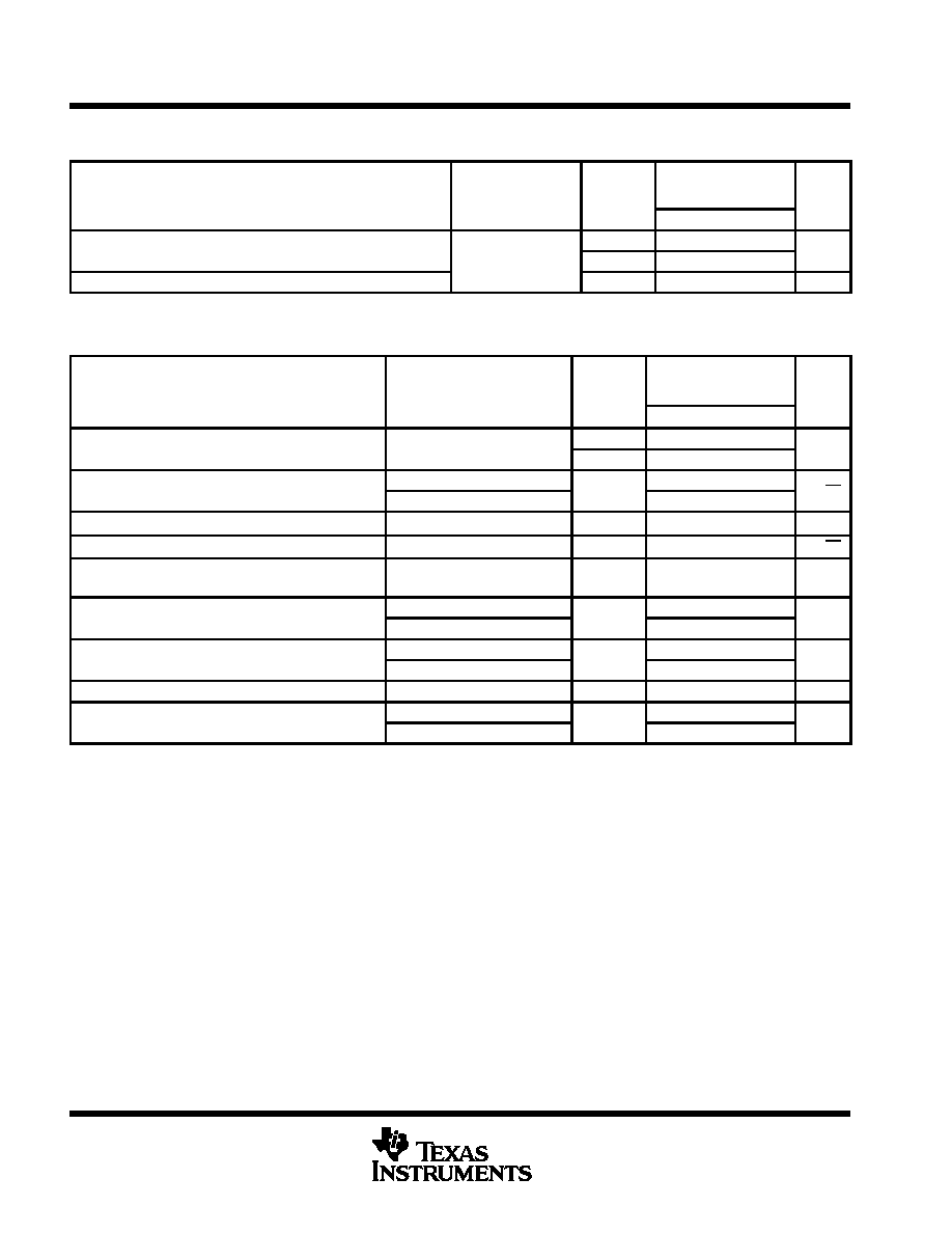
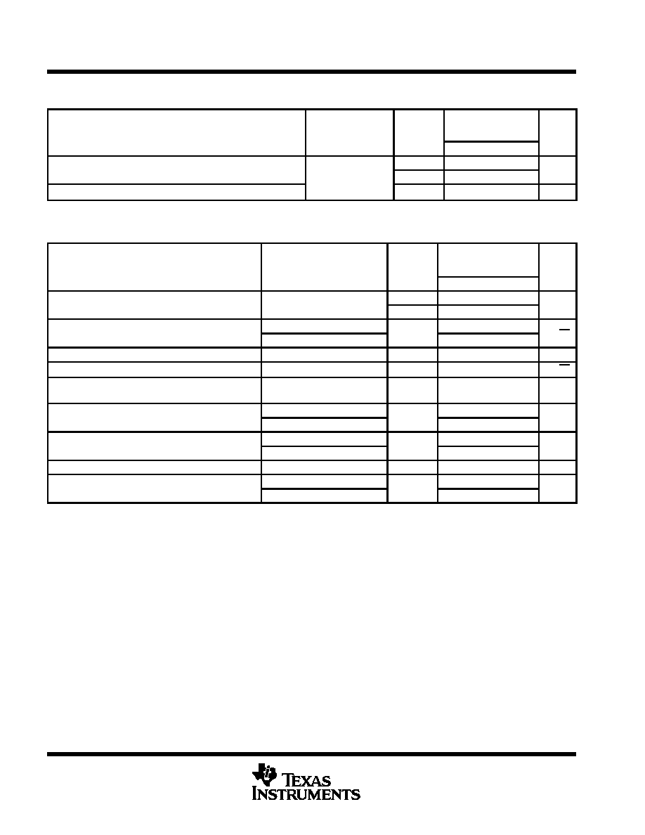
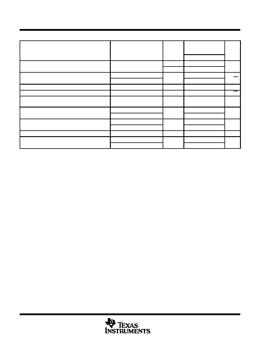
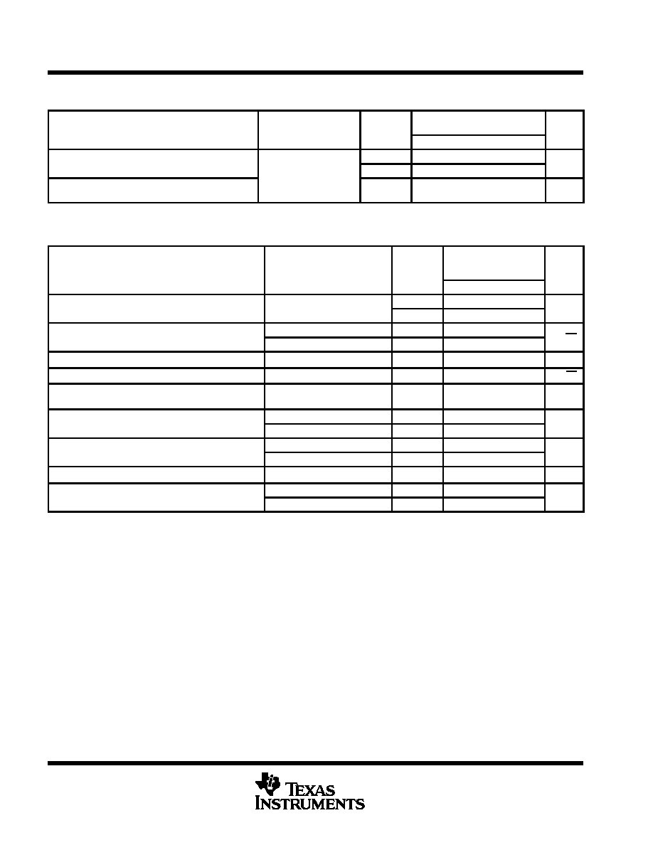
TLE2061C electrical characteristics at specified free-air temperature, V
CC
±
=
±
5 V (unless
otherwise noted)
PARAMETER
TEST CONDITIONS
TA
TLE2061C
TLE2061AC
TLE2061BC
UNIT
MIN
TYP
MAX
TLE2061C
25
∞
C
0.8
3.1
TLE2061C
Full range
4
VIO
Input offset voltage
TLE2061AC
25
∞
C
0.6
2.6
mV
VIO
Input offset voltage
TLE2061AC
Full range
3.5
mV
TLE2061BC
25
∞
C
0.5
1.9
TLE2061BC
VIC = 0
RS = 50
Full range
2.4
VIO
Temperature coefficient of input offset voltage
VIC = 0,
RS = 50
Full range
6
µ
V/
∞
C
Input offset voltage long-term drift (see Note 4)
25
∞
C
0.04
µ
V/mo
IIO
Input offset current
25
∞
C
1
pA
IIO
Input offset current
Full range
0.8
nA
IIB
Input bias current
25
∞
C
3
pA
IIB
Input bias current
Full range
2
nA
VICR
Common mode input voltage range
25
∞
C
≠ 1.6
to
4
≠ 2
to
6
V
VICR
Common-mode input voltage range
Full range
≠ 1.6
to
4
V
RL = 10 k
25
∞
C
3.5
3.7
VOM
Maximum positive peak output voltage swing
RL = 10 k
Full range
3.3
V
VOM + Maximum positive peak output voltage swing
RL = 100
25
∞
C
2.5
3.1
V
RL = 100
Full range
2
RL = 10 k
25
∞
C
≠ 3.7
≠ 3.9
VOM
Maximum negative peak output voltage swing
RL = 10 k
Full range
≠ 3.3
V
VOM ≠ Maximum negative peak output voltage swing
RL = 100
25
∞
C
≠ 2.5
≠ 2.7
V
RL = 100
Full range
≠ 2
VO =
±
2 8 V
RL = 10 k
25
∞
C
15
80
VO =
±
2.8 V,
RL = 10 k
Full range
2
AVD
Large signal differential voltage amplification
VO = 0 to 2 V
RL = 100
25
∞
C
0.75
45
V/mV
AVD
Large-signal differential voltage amplification
VO = 0 to 2 V,
RL = 100
Full range
0.5
V/mV
VO = 0 to 2 V RL = 100
25
∞
C
0.5
3
VO = 0 to ≠ 2 V, RL = 100
Full range
0.25
ri
Input resistance
25
∞
C
1012
ci
Input capacitance
25
∞
C
4
pF
zo
Open-loop output impedance
IO = 0
25
∞
C
280
CMRR
Common mode rejection ratio
VIC = VICRmin RS = 50
25
∞
C
65
82
dB
CMRR
Common-mode rejection ratio
VIC = VICRmin, RS = 50
Full range
65
dB
kSVR
Supply voltage rejection ratio (
VCC
±
/
VIO)
VCC
±
=
±
5 V to
±
15 V,
25
∞
C
75
93
dB
kSVR
Supply-voltage rejection ratio (
VCC
±
/
VIO)
CC
±
,
RS = 50
Full range
75
dB
Full range is 0
∞
C to 70
∞
C.
NOTE 4: Typical values are based on the input offset voltage shift observed through 168 hours of operating life test at TA = 150
∞
C extrapolated
to TA = 25
∞
C using the Arrhenius equation and assuming an activation energy of 0.96 eV.
TLE206x, TLE206xA, TLE206xB, TLE206xY
EXCALIBUR JFET-INPUT HIGH-OUTPUT-DRIVE
µ
POWER OPERATIONAL AMPLIFIERS
SLOS193A ≠ FEBRUARY 1997 ≠ REVISED MARCH 1998
10
POST OFFICE BOX 655303
∑
DALLAS, TEXAS 75265
TLE2061C electrical characteristics at specified free-air temperature, V
CC
±
=
±
5 V (unless
otherwise noted) (continued)
PARAMETER
TEST CONDITIONS
TA
TLE2061C
TLE2061AC
TLE2061BC
UNIT
MIN
TYP
MAX
ICC
Supply current
25
∞
C
280
325
µ
A
ICC
Supply current
VO = 0,
No load
Full range
350
µ
A
ICC
Supply-current change over operating temperature range
Full range
29
µ
A
Full range is 0
∞
C to 70
∞
C.
TLE2061C operating characteristics at specified free-air temperature, V
CC
±
=
±
5 V
PARAMETER
TEST CONDITIONS
TA
TLE2061C
TLE2061AC
TLE2061BC
UNIT
MIN
TYP
MAX
SR
Slew rate at unity gain (see Figure 1)
RL = 10 k
CL = 100 pF
25
∞
C
2.2
3.4
V/
µ
s
SR
Slew rate at unity gain (see Figure 1)
RL = 10 k
,
CL = 100 pF
Full range
2.1
V/
µ
s
V
Equivalent input noise voltage (see Figure 2)
f = 10 Hz,
RS = 20
25
∞
C
59
100
nV/
Hz
Vn
Equivalent input noise voltage (see Figure 2)
f = 1 kHz ,
RS = 20
25
∞
C
43
60
nV/
Hz
VN(PP) Peak to peak equivalent input noise voltage
f = 0 1 Hz to 10 Hz
25
∞
C
1 1
µ
V
VN(PP) Peak-to-peak equivalent input noise voltage
f = 0.1 Hz to 10 Hz
25
∞
C
1.1
µ
V
In
Equivalent input noise current
f = 1 kHz
25
∞
C
1
fA/
Hz
THD
Total harmonic distortion
AVD
= 2,
f = 10 kHz,
25
∞
C
0 025%
THD
Total harmonic distortion
VD
,
,
VO(PP) = 2 V, RL = 10 k
25
∞
C
0.025%
B1
Unity gain bandwidth (see Figure 3)
RL = 10 k
,
CL = 100 pF
25
∞
C
1.8
MHz
B1
Unity-gain bandwidth (see Figure 3)
RL
= 100
,
CL = 100 pF
25
∞
C
1.3
MHz
t
Settling time
0.1%
25
∞
C
5
µ
s
ts
Settling time
0.01%
25
∞
C
10
µ
s
BOM
Maximum output-swing bandwidth
AVD = 1,
RL
= 10 k
25
∞
C
140
kHz
Phase margin at unity gain (see Figure 3)
RL
= 10 k
,
CL = 100 pF
25
∞
C
58
∞
m
Phase margin at unity gain (see Figure 3)
RL
= 100
,
CL = 100 pF
25
∞
C
75
∞
Full range is 0
∞
C to 70
∞
C.
TLE206x, TLE206xA, TLE206xB, TLE206xY
EXCALIBUR JFET-INPUT HIGH-OUTPUT-DRIVE
µ
POWER OPERATIONAL AMPLIFIERS
SLOS193A ≠ FEBRUARY 1997 ≠ REVISED MARCH 1998
11
POST OFFICE BOX 655303
∑
DALLAS, TEXAS 75265
TLE2061C electrical characteristics at specified free-air temperature, V
CC
±
=
±
15 V (unless
otherwise noted)
PARAMETER
TEST CONDITIONS
TA
TLE2061C
TLE2061AC
TLE2061BC
UNIT
MIN
TYP
MAX
TLE2061C
25
∞
C
0.6
3
TLE2061C
Full range
3.9
VIO
Input offset voltage
TLE2061AC
25
∞
C
0.5
1.5
mV
VIO
Input offset voltage
TLE2061AC
Full range
2.5
mV
TLE2061BC
25
∞
C
0.3
0.5
TLE2061BC
VIC = 0
RS = 50 k
Full range
1
VIO
Temperature coefficient of input offset voltage
VIC = 0,
RS = 50 k
Full range
6
µ
V/
∞
C
Input offset voltage long-term drift (see Note 4)
25
∞
C
0.04
µ
V/mo
IIO
Input offset current
25
∞
C
2
pA
IIO
Input offset current
Full range
1
nA
IIB
Input bias current
25
∞
C
4
pA
IIB
Input bias current
Full range
3
nA
VICR
Common mode input voltage range
25
∞
C
≠ 11
to
13
≠ 12
to
16
V
VICR
Common-mode input voltage range
Full range
≠ 11
to
13
V
RL = 10 k
25
∞
C
13.2
13.7
VOM
Maximum positive peak output voltage swing
RL = 10 k
Full range
13
V
VOM + Maximum positive peak output voltage swing
RL = 600
25
∞
C
12.5
13.2
V
RL = 600
Full range
12
RL = 10 k
25
∞
C
≠13.2
≠ 13.7
VOM
Maximum negative peak output voltage swing
RL = 10 k
Full range
≠ 13
V
VOM ≠ Maximum negative peak output voltage swing
RL = 600
25
∞
C
≠ 12.5
≠ 13
V
RL = 600
Full range
≠ 12
VO =
±
10 V
RL = 10 k
25
∞
C
30
230
VO =
±
10 V,
RL = 10 k
Full range
20
AVD
Large signal differential voltage amplification
VO = 0 to 8 V
RL = 600
25
∞
C
25
100
V/mV
AVD
Large-signal differential voltage amplification
VO = 0 to 8 V,
RL = 600
Full range
10
V/mV
VO = 0 to 8 V RL = 600
25
∞
C
3
25
VO = 0 to ≠ 8 V, RL = 600
Full range
1
ri
Input resistance
25
∞
C
1012
ci
Input capacitance
25
∞
C
4
pF
zo
Open-loop output impedance
IO = 0
25
∞
C
280
CMRR
Common mode rejection ratio
VIC = VICRmin RS = 50
25
∞
C
72
90
dB
CMRR
Common-mode rejection ratio
VIC = VICRmin, RS = 50
Full range
70
dB
kSVR
Supply voltage rejection ratio (
VCC
±
/
VIO)
VCC
±
=
±
5 V to
±
15 V,
25
∞
C
75
93
dB
kSVR
Supply-voltage rejection ratio (
VCC
±
/
VIO)
CC
±
,
RS = 50
Full range
75
dB
Full range is 0
∞
C to 70
∞
C.
NOTE 4: Typical values are based on the input offset voltage shift observed through 168 hours of operating life test at TA = 150
∞
C extrapolated
to TA = 25
∞
C using the Arrhenius equation and assuming an activation energy of 0.96 eV.
TLE206x, TLE206xA, TLE206xB, TLE206xY
EXCALIBUR JFET-INPUT HIGH-OUTPUT-DRIVE
µ
POWER OPERATIONAL AMPLIFIERS
SLOS193A ≠ FEBRUARY 1997 ≠ REVISED MARCH 1998
12
POST OFFICE BOX 655303
∑
DALLAS, TEXAS 75265
TLE2061C electrical characteristics at specified free-air temperature, V
CC
±
=
±
15 V (unless
otherwise noted) (continued)
PARAMETER
TEST CONDITIONS
TA
TLE2061C
TLE2061AC
TLE2061BC
UNIT
MIN
TYP
MAX
ICC
Supply current
25
∞
C
290
350
µ
A
ICC
Supply current
VO = 0, No load
Full range
375
µ
A
ICC
Supply current change over operating temperature range
O
Full range
34
µ
A
ICC
Supply-current change over operating temperature range
Full range
34
µ
A
Full range is 0
∞
C to 70
∞
C.
TLE2061C operating characteristics at specified free-air temperature, V
CC
±
=
±
15 V
PARAMETER
TEST CONDITIONS
TA
TLE2061C
TLE2061AC
TLE2061BC
UNIT
MIN
TYP
MAX
SR
Slew rate at unity gain (see Figure 1)
RL = 10 k
CL = 100 pF
25
∞
C
2.6
3.4
V/
µ
s
SR
Slew rate at unity gain (see Figure 1)
RL = 10 k
,
CL = 100 pF
Full range
2.5
V/
µ
s
V
Equivalent input noise voltage (see Figure 2)
f = 10 Hz,
RS = 20
25
∞
C
70
100
nV/
Hz
Vn
Equivalent input noise voltage (see Figure 2)
f = 1 kHz ,
RS = 20
25
∞
C
40
60
nV/
Hz
VN(PP) Peak-to-peak equivalent input noise voltage
f = 0.1 Hz to 10 Hz
25
∞
C
1.1
µ
V
In
Equivalent input noise current
f = 1 kHz
25
∞
C
1.1
fA/
Hz
THD
Total harmonic distortion
AVD
= 2,
f = 10 kHz,
25
∞
C
0 025%
THD
Total harmonic distortion
VD
,
,
VO(PP) = 2 V,
RL = 10 k
25
∞
C
0.025%
B1
Unity gain bandwidth (see Figure 3)
RL = 10 k
,
CL = 100 pF
25
∞
C
2
MHz
B1
Unity-gain bandwidth (see Figure 3)
RL
= 600
,
CL = 100 pF
25
∞
C
1.5
MHz
t
Settling time
0.1%
25
∞
C
5
µ
s
ts
Settling time
0.01%
25
∞
C
10
µ
s
BOM
Maximum output-swing bandwidth
AVD = 1,
RL
= 10 k
25
∞
C
40
kHz
Phase margin at unity gain (see Figure 3)
RL
= 10 k
,
CL = 100 pF
25
∞
C
60
∞
m
Phase margin at unity gain (see Figure 3)
RL
= 600
,
CL = 100 pF
25
∞
C
70
∞
Full range is 0
∞
C to 70
∞
C.
TLE206x, TLE206xA, TLE206xB, TLE206xY
EXCALIBUR JFET-INPUT HIGH-OUTPUT-DRIVE
µ
POWER OPERATIONAL AMPLIFIERS
SLOS193A ≠ FEBRUARY 1997 ≠ REVISED MARCH 1998
13
POST OFFICE BOX 655303
∑
DALLAS, TEXAS 75265
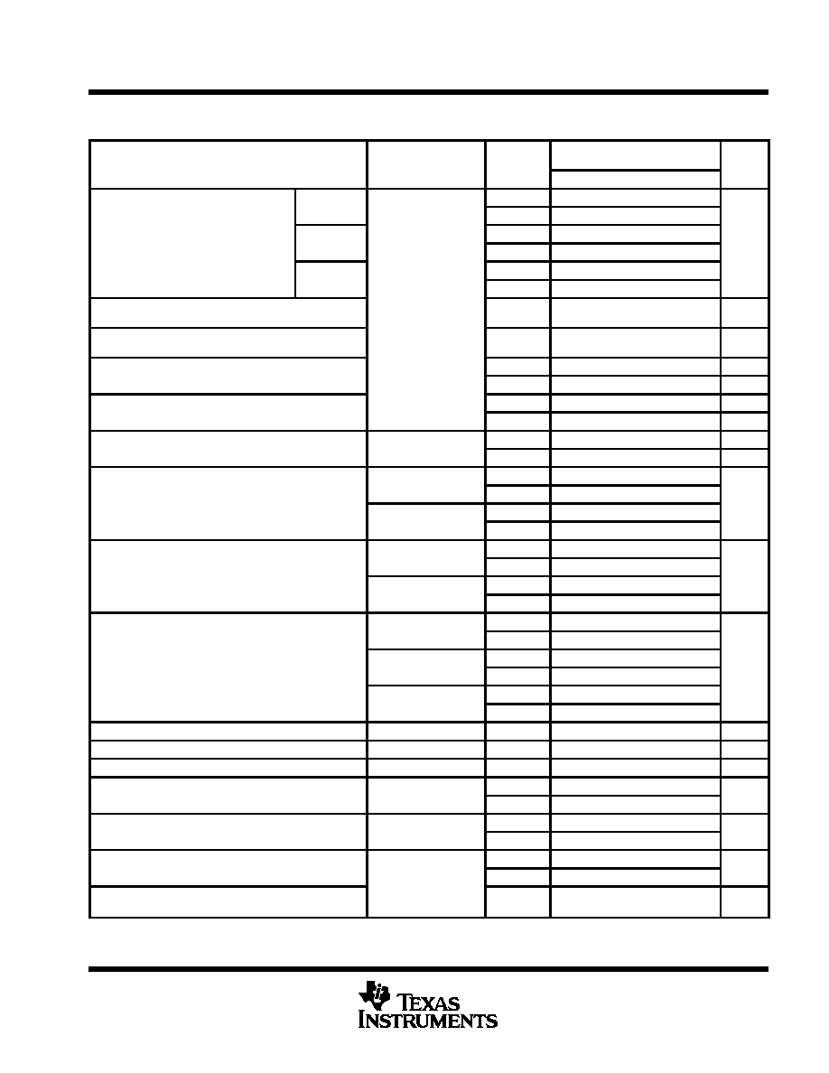
TLE2061I electrical characteristics at specified free-air temperature, V
CC
±
=
±
5 V (unless otherwise
noted)
PARAMETER
TEST CONDITIONS
TA
TLE2061I , TLE2061AI
TLE2061BI
UNIT
TA
MIN
TYP
MAX
TLE2061I
25
∞
C
0.8
3.1
TLE2061I
Full range
4.4
VIO
Input offset voltage
TLE2061AI
25
∞
C
0.6
2.6
mV
VIO
Input offset voltage
TLE2061AI
Full range
3.9
mV
TLE2061BI
25
∞
C
0.5
1.9
TLE2061BI
VIC = 0,
Full range
2.7
VIO
Temperature coefficient of input offset voltage
VIC 0,
RS = 50
Full range
6
µ
V/
∞
C
Input offset voltage long-term drift (see Note 4)
25
∞
C
0.04
µ
V/mo
IIO
Input offset current
25
∞
C
1
pA
IIO
Input offset current
Full range
2
nA
IIB
Input bias current
25
∞
C
3
pA
IIB
Input bias current
Full range
4
nA
VICR
Common mode input voltage range
25
∞
C
≠ 1.6 to 4
≠ 2 to 6
V
VICR
Common-mode input voltage range
Full range
≠ 1.6 to 4
V
RL = 10 k
25
∞
C
3.5
3.7
VOM
Maximum positive peak output voltage swing
RL = 10 k
Full range
3.1
V
VOM +
Maximum positive peak output voltage swing
RL = 100
25
∞
C
2.5
3.1
V
RL = 100
Full range
2
RL = 10 k
25
∞
C
≠3.7
≠ 3.9
VOM
Maximum negative peak output voltage swing
RL = 10 k
Full range
≠ 3.1
V
VOM ≠
Maximum negative peak output voltage swing
RL = 100
25
∞
C
≠ 2.5
≠ 2.7
V
RL = 100
Full range
≠ 2
VO =
±
2.8 V,
25
∞
C
15
80
VO
±
2.8 V,
RL = 10 k
Full range
2
AVD
Large signal differential voltage amplification
VO = 0 to 2 V,
25
∞
C
0.75
45
V/mV
AVD
Large-signal differential voltage amplification
VO 0 to 2 V,
RL = 100
Full range
0.5
V/mV
VO = 0 to ≠ 2 V,
25
∞
C
0.5
3
VO 0 to 2 V,
RL = 100
Full range
0.25
ri
Input resistance
25
∞
C
1012
ci
Input capacitance
25
∞
C
4
pF
zo
Open-loop output impedance
IO = 0
25
∞
C
280
CMRR
Common mode rejection ratio
VIC = VICRmin,
25
∞
C
65
82
dB
CMRR
Common-mode rejection ratio
IC
ICR
,
RS = 50
Full range
65
dB
kSVR
Supply voltage rejection ratio (
VCC
±
/
VIO)
VCC
±
=
±
5 V to
±
15 V,
25
∞
C
75
93
dB
kSVR
Supply-voltage rejection ratio (
VCC
±
/
VIO)
CC
±
RS = 50
Full range
65
dB
ICC
Supply current
25
∞
C
280
325
µ
A
ICC
Supply current
VO = 0,
N l
d
Full range
350
µ
A
ICC
Supply-current change over operating
temperature range
No load
Full range
29
µ
A
Full range is ≠ 40
∞
C to 85
∞
C.
NOTE 4: Typical values are based on the input offset voltage shift observed through 168 hours of operating life test at TA = 150
∞
C extrapolated
to TA = 25
∞
C using the Arrhenius equation and assuming an activation energy of 0.96 eV.
TLE206x, TLE206xA, TLE206xB, TLE206xY
EXCALIBUR JFET-INPUT HIGH-OUTPUT-DRIVE
µ
POWER OPERATIONAL AMPLIFIERS
SLOS193A ≠ FEBRUARY 1997 ≠ REVISED MARCH 1998
14
POST OFFICE BOX 655303
∑
DALLAS, TEXAS 75265
TLE2061I operating characteristics at specified free-air temperature, V
CC
±
=
±
5 V
PARAMETER
TEST CONDITIONS
TA
TLE2061I
TLE2061AI
TLE2061BI
UNIT
MIN
TYP
MAX
SR
Slew rate at unity gain (see Figure 1)
RL = 10 k
CL = 100 pF
25
∞
C
2.2
3.4
V/
µ
s
SR
Slew rate at unity gain (see Figure 1)
RL = 10 k
,
CL = 100 pF
Full range
1.7
V/
µ
s
V
Equivalent input noise voltage (see Figure 2)
f = 10 Hz,
RS = 20
25
∞
C
59
100
nV/
Hz
Vn
Equivalent input noise voltage (see Figure 2)
f = 1 kHz ,
RS = 20
25
∞
C
43
60
nV/
Hz
VN(PP) Peak-to-peak equivalent input noise voltage
f = 0.1 Hz to 10 Hz
25
∞
C
1.1
µ
V
In
Equivalent input noise current
f = 1 kHz
25
∞
C
1
fA/
Hz
THD
Total harmonic distortion
AVD
= 2,
f = 10 kHz,
25
∞
C
0 025%
THD
Total harmonic distortion
VD
,
,
VO(PP) = 2 V,
RL = 10 k
25
∞
C
0.025%
B1
Unity gain bandwidth (see Figure 3)
RL = 10 k
,
CL = 100 pF
25
∞
C
1.8
MHz
B1
Unity-gain bandwidth (see Figure 3)
RL
= 100
,
CL = 100 pF
25
∞
C
1.3
MHz
t
Settling time
0.1%
25
∞
C
5
µ
s
ts
Settling time
0.01%
25
∞
C
10
µ
s
BOM
Maximum output-swing bandwidth
AVD = 1,
RL
= 10 k
25
∞
C
140
kHz
Phase margin at unity gain (see Figure 3)
RL
= 10 k
,
CL = 100 pF
25
∞
C
58
∞
m
Phase margin at unity gain (see Figure 3)
RL
= 100
,
CL = 100 pF
25
∞
C
75
∞
Full range is ≠ 40
∞
C to 85
∞
C.
TLE206x, TLE206xA, TLE206xB, TLE206xY
EXCALIBUR JFET-INPUT HIGH-OUTPUT-DRIVE
µ
POWER OPERATIONAL AMPLIFIERS
SLOS193A ≠ FEBRUARY 1997 ≠ REVISED MARCH 1998
15
POST OFFICE BOX 655303
∑
DALLAS, TEXAS 75265
TLE2061I electrical characteristics at specified free-air temperature, V
CC
±
=
±
15 V (unless
otherwise noted)
PARAMETER
TEST CONDITIONS
TA
TLE2061I, TLE2061AI
TLE2061BI
UNIT
TA
MIN
TYP
MAX
TLE2061I
25
∞
C
0.6
3
TLE2061I
Full range
4.3
VIO
Input offset voltage
TLE2061AI
25
∞
C
0.5
1.5
mV
VIO
Input offset voltage
TLE2061AI
Full range
2.9
mV
TLE2061BI
25
∞
C
0.3
0.5
TLE2061BI
Full range
1.3
VIO
Temperature coefficient of input offset
voltage
VIC = 0,
RS = 50
Full range
6
µ
V/
∞
C
Input offset voltage long-term drift
(see Note 4)
25
∞
C
0.04
µ
V/mo
IIO
Input offset current
25
∞
C
2
pA
IIO
Input offset current
Full range
3
nA
IIB
Input bias current
25
∞
C
4
pA
IIB
Input bias current
Full range
5
nA
VICR
Common mode input voltage range
25
∞
C
≠ 11 to 13
≠ 12 to 16
V
VICR
Common-mode input voltage range
Full range
≠ 11 to 13
V
RL = 10 k
25
∞
C
13.2
13.7
VOM
Maximum positive peak output voltage swing
RL = 10 k
Full range
13
V
VOM +
Maximum positive peak output voltage swing
RL = 600
25
∞
C
12.5
13.2
V
RL = 600
Full range
12
RL = 10 k
25
∞
C
≠13.2
≠ 13.7
VOM
Maximum negative peak output voltage
RL = 10 k
Full range
≠ 13
V
VOM ≠
Maximum negative eak out ut voltage
swing
RL = 600
25
∞
C
≠ 12.5
≠ 13
V
RL = 600
Full range
≠ 12
VO =
±
10 V,
25
∞
C
30
230
VO
±
10 V,
RL = 10 k
Full range
20
AVD
Large signal differential voltage amplification
VO = 0 to 8 V,
25
∞
C
25
100
V/mV
AVD
Large-signal differential voltage amplification
VO 0 to 8 V,
RL = 600
Full range
10
V/mV
VO = 0 to ≠ 8 V,
25
∞
C
3
25
VO 0 to 8 V,
RL = 600
Full range
01
ri
Input resistance
25
∞
C
1012
ci
Input capacitance
25
∞
C
4
pF
zo
Open-loop output impedance
IO = 0
25
∞
C
280
CMRR
Common mode rejection ratio
VIC = VICRmin,
25
∞
C
72
90
dB
CMRR
Common-mode rejection ratio
VIC VICRmin,
RS = 50
Full range
65
dB
kSVR
Supply voltage rejection ratio (
VCC
±
/
VIO)
VCC
±
=
±
5 V to
±
15 V,
25
∞
C
75
93
dB
kSVR
Supply-voltage rejection ratio (
VCC
±
/
VIO)
CC
±
,
RS = 50
Full range
65
dB
ICC
Supply current
25
∞
C
290
350
µ
A
ICC
Supply current
VO = 0,
Full range
375
µ
A
ICC
Supply-current change over operating
temperature range
O
No load
Full range
34
µ
A
Full range is ≠ 40
∞
C to 85
∞
C.
NOTE 4: Typical values are based on the input offset voltage shift observed through 168 hours of operating life test at TA = 150
∞
C extrapolated
to TA = 25
∞
C using the Arrhenius equation and assuming an activation energy of 0.96 eV.
TLE206x, TLE206xA, TLE206xB, TLE206xY
EXCALIBUR JFET-INPUT HIGH-OUTPUT-DRIVE
µ
POWER OPERATIONAL AMPLIFIERS
SLOS193A ≠ FEBRUARY 1997 ≠ REVISED MARCH 1998
16
POST OFFICE BOX 655303
∑
DALLAS, TEXAS 75265
TLE2061I operating characteristics at specified free-air temperature, V
CC
±
=
±
15 V
PARAMETER
TEST CONDITIONS
TA
TLE2061I
TLE2061AI
TLE2061BI
UNIT
MIN
TYP
MAX
SR
Slew rate at unity gain (see Figure 1)
RL = 10 k
CL = 100 pF
25
∞
C
2.6
3.4
V/
µ
s
SR
Slew rate at unity gain (see Figure 1)
RL = 10 k
,
CL = 100 pF
Full range
2.1
V/
µ
s
V
Equivalent input noise voltage (see Figure 2)
f = 10 Hz,
RS = 20
25
∞
C
70
100
nV/
Hz
Vn
Equivalent input noise voltage (see Figure 2)
f = 1 kHz ,
RS = 20
25
∞
C
40
60
nV/
Hz
VN(PP) Peak-to-peak equivalent input noise voltage
f = 0.1 Hz to 10 Hz
25
∞
C
1.1
µ
V
In
Equivalent input noise current
f = 1 kHz
25
∞
C
1.1
fA/
Hz
THD
Total harmonic distortion
AVD
= 2,
f = 10 kHz,
25
∞
C
0 025%
THD
Total harmonic distortion
VD
,
,
VO(PP) = 2 V,
RL = 10 k
25
∞
C
0.025%
B1
Unity gain bandwidth (see Figure 3)
RL = 10 k
,
CL = 100 pF
25
∞
C
2
MHz
B1
Unity-gain bandwidth (see Figure 3)
RL
= 600
,
CL = 100 pF
25
∞
C
1.5
MHz
t
Settling time
0.1%
25
∞
C
5
µ
s
ts
Settling time
0.01%
25
∞
C
10
µ
s
BOM
Maximum output-swing bandwidth
AVD = 1,
RL
= 10 k
25
∞
C
40
kHz
Phase margin at unity gain (see Figure 3)
RL
= 10 k
,
CL = 100 pF
25
∞
C
60
∞
m
Phase margin at unity gain (see Figure 3)
RL
= 600
,
CL = 100 pF
25
∞
C
70
∞
Full range is ≠ 40
∞
C to 85
∞
C.
TLE206x, TLE206xA, TLE206xB, TLE206xY
EXCALIBUR JFET-INPUT HIGH-OUTPUT-DRIVE
µ
POWER OPERATIONAL AMPLIFIERS
SLOS193A ≠ FEBRUARY 1997 ≠ REVISED MARCH 1998
17
POST OFFICE BOX 655303
∑
DALLAS, TEXAS 75265
TLE2061M electrical characteristics at specified free-air temperature, V
CC
±
=
±
5 V (unless
otherwise noted)
PARAMETER
TEST CONDITIONS
TA
TLE2061M
TLE2061AM
TLE2061BM
UNIT
MIN
TYP
MAX
TLE2061M
25
∞
C
0.8
3.1
TLE2061M
Full range
6
VIO
Input offset voltage
TLE2061AM
25
∞
C
0.6
2.6
mV
VIO
Input offset voltage
TLE2061AM
Full range
4.6
mV
TLE2061BM
25
∞
C
0.5
1.9
TLE2061BM
VIC = 0
RS = 50
Full range
3.1
VIO
Temperature coefficient of input offset voltage
VIC = 0,
RS = 50
Full range
6
µ
V/
∞
C
Input offset voltage long-term drift (see Note 4)
25
∞
C
0.04
µ
V/mo
IIO
Input offset current
25
∞
C
1
pA
IIO
Input offset current
Full range
15
nA
IIB
Input bias current
25
∞
C
3
pA
IIB
Input bias current
Full range
30
nA
VICR
Common mode input voltage range
25
∞
C
≠ 1.6
to
4
≠ 2
to
6
V
VICR
Common-mode input voltage range
Full range
≠ 1.6
to
4
V
RL = 10 k
25
∞
C
3.5
3.7
RL = 10 k
Full range
3
VOM
Maximum positive peak output voltage swing
RL = 600
25
∞
C
2.5
3.6
V
VOM + Maximum positive peak output voltage swing
RL = 600
Full range
2
V
RL = 100
25
∞
C
2.5
3.1
RL = 100
Full range
2
RL = 10 k
25
∞
C
≠ 3.5
≠ 3.9
RL = 10 k
Full range
≠ 3
VOM
Maximum negative peak
FK and JG
RL = 600
25
∞
C
≠ 2.5
≠ 3.5
V
VOM ≠
g
output voltage swing
packages
RL = 600
Full range
≠ 2
V
D and P
RL = 100
25
∞
C
≠ 2.5
≠ 2.7
packages
RL = 100
Full range
≠ 2
VO =
±
2 8 V
RL = 10 k
25
∞
C
15
80
VO =
±
2.8 V,
RL = 10 k
Full range
2
VO = 0 to 2 5 V RL = 600
25
∞
C
1
65
FK and JG
VO = 0 to 2.5 V, RL = 600
Full range
0.5
AVD
Large-signal differential
packages
VO = 0 to 2 5 V RL = 600
25
∞
C
1
16
V/mV
AVD
g
g
voltage amplification
VO = 0 to ≠ 2.5 V,RL = 600
Full range
0.5
V/mV
VO = 0 to 2 V
RL = 100
25
∞
C
0.75
45
D and P
VO = 0 to 2 V,
RL = 100
Full range
0.5
packages
VO = 0 to 2 V RL = 100
25
∞
C
0.5
3
VO = 0 to ≠ 2 V, RL = 100
Full range
0.25
Full range is ≠ 55
∞
C to 125
∞
C.
NOTE 4: Typical values are based on the input offset voltage shift observed through 168 hours of operating life test at TA = 150
∞
C extrapolated
to TA = 25
∞
C using the Arrhenius equation and assuming an activation energy of 0.96 eV.
TLE206x, TLE206xA, TLE206xB, TLE206xY
EXCALIBUR JFET-INPUT HIGH-OUTPUT-DRIVE
µ
POWER OPERATIONAL AMPLIFIERS
SLOS193A ≠ FEBRUARY 1997 ≠ REVISED MARCH 1998
18
POST OFFICE BOX 655303
∑
DALLAS, TEXAS 75265
TLE2061M electrical characteristics at specified free-air temperature, V
CC
±
=
±
5 V (unless
otherwise noted) (continued)
PARAMETER
TEST CONDITIONS
TA
TLE2061M
TLE2061AM
TLE2061BM
UNIT
MIN
TYP
MAX
ri
Input resistance
25
∞
C
1012
ci
Input capacitance
25
∞
C
4
pF
zo
Open-loop output impedance
IO = 0
25
∞
C
280
CMRR
Common mode rejection ratio
VIC = VICRmin,
25
∞
C
65
82
dB
CMRR
Common-mode rejection ratio
IC
ICR
,
RS = 50
Full range
60
dB
kSVR
Supply-voltage rejection ratio (
VCC
±
/
VIO)
VCC
±
=
±
5 V to
±
15 V,
25
∞
C
75
93
dB
kSVR
Su
ly-voltage rejection ratio (
VCC
±
/
VIO)
RS = 50
Full range
65
dB
ICC
Supply current
25
∞
C
280
325
µ
A
ICC
Supply current
VO = 0
No load
Full range
350
µ
A
ICC
Supply-current change over operating
temperature range
VO = 0,
No load
Full range
39
µ
A
Full range is ≠ 55
∞
C to 125
∞
C.
TLE2061M operating characteristics at specified free-air temperature, V
CC
±
=
±
5 V, T
A
= 25
∞
C
PARAMETER
TEST CONDITIONS
TLE2061M
TLE2061AM
TLE2061BM
UNIT
MIN
TYP
MAX
SR
Slew rate at unity gain (see Figure 1)
RL = 10 k
CL = 100 pF
3 4
V/
µ
s
SR
Slew rate at unity gain (see Figure 1)
RL = 10 k
,
CL = 100 pF
3.4
V/
µ
s
V
Equivalent input noise voltage (see Figure 2)
f = 10 Hz,
RS = 20
59
nV/
Hz
Vn
Equivalent input noise voltage (see Figure 2)
f = 1 kHz ,
RS = 20
43
nV/
Hz
VN(PP) Peak to peak equivalent input noise voltage
f = 0 1 Hz to 10 Hz
1 1
µ
V
VN(PP) Peak-to-peak equivalent input noise voltage
f = 0.1 Hz to 10 Hz
1.1
µ
V
In
Equivalent input noise current
f = 1 kHz
1
fA /
Hz
THD
Total harmonic distortion
AVD
= 2,
f = 10 kHz,
0 025%
THD
Total harmonic distortion
VD
,
,
VO(PP) = 2 V,
RL = 10 k
0.025%
B1
Unity gain bandwidth (see Figure 3)
RL = 10 k
,
CL = 100 pF
1.8
MHz
B1
Unity-gain bandwidth (see Figure 3)
RL
= 600
,
CL = 100 pF
1.3
MHz
t
Settling time
0.1%
5
µ
s
ts
Settling time
0.01%
10
µ
s
BOM
Maximum output-swing bandwidth
AVD = 1,
RL
= 10 k
140
kHz
Phase margin at unity gain (see Figure 3)
RL
= 10 k
,
CL = 100 pF
58
∞
m
Phase margin at unity gain (see Figure 3)
RL
= 600
,
CL = 100 pF
75
∞
TLE206x, TLE206xA, TLE206xB, TLE206xY
EXCALIBUR JFET-INPUT HIGH-OUTPUT-DRIVE
µ
POWER OPERATIONAL AMPLIFIERS
SLOS193A ≠ FEBRUARY 1997 ≠ REVISED MARCH 1998
19
POST OFFICE BOX 655303
∑
DALLAS, TEXAS 75265
TLE2061M electrical characteristics at specified free-air temperature, V
CC
±
=
±
15 V (unless
otherwise noted)
PARAMETER
TEST CONDITIONS
TA
TLE2061M ,TLE2061AM
TLE2061BM
UNIT
TA
MIN
TYP
MAX
TLE2061M
25
∞
C
0.6
3
TLE2061M
Full range
6
VIO
Input offset voltage
TLE2061AM
25
∞
C
0.5
1.5
mV
VIO
Input offset voltage
TLE2061AM
Full range
3.6
mV
TLE2061BM
25
∞
C
0.3
0.5
TLE2061BM
Full range
1.7
VIO
Temperature coefficient of input offset
voltage
VIC = 0,
RS = 50
Full range
6
µ
V/
∞
C
Input offset voltage long-term drift
(see Note 4)
25
∞
C
0.04
µ
V/mo
IIO
Input offset current
25
∞
C
2
pA
IIO
Input offset current
Full range
20
nA
IIB
Input bias current
25
∞
C
4
pA
IIB
Input bias current
Full range
40
nA
VICR
Common mode input voltage range
25
∞
C
≠ 11 to 13
≠ 12 to 16
V
VICR
Common-mode input voltage range
Full range
≠ 11 to 13
V
RL = 10 k
25
∞
C
13
13.7
VOM
Maximum positive peak output voltage
RL = 10 k
Full range
12.5
V
VOM +
Maximum ositive eak out ut voltage
swing
RL = 600
25
∞
C
12.5
13.2
V
RL = 600
Full range
12
RL = 10 k
25
∞
C
≠ 13
≠ 13.7
VOM
Maximum negative peak output voltage
RL = 10 k
Full range
≠ 12.5
V
VOM ≠
Maximum negative eak out ut voltage
swing
RL = 600
25
∞
C
≠ 12.5
≠ 13
V
RL = 600
Full range
≠ 12
VO =
±
10 V,
25
∞
C
30
230
VO
±
10 V,
RL = 10 k
Full range
20
AVD
Large-signal differential voltage VO = 0 to 8 V,
25
∞
C
25
100
V/mV
AVD
Large signal differential voltage
amplification
VO 0 to 8 V,
RL = 600
Full range
7
V/mV
VO = 0 to ≠ 8 V,
25
∞
C
3
25
VO 0 to 8 V,
RL = 600
Full range
1
ri
Input resistance
25
∞
C
1012
ci
Input capacitance
25
∞
C
4
pF
zo
Open-loop output impedance
IO = 0
25
∞
C
280
CMRR
Common mode rejection ratio
VIC = VICRmin,
25
∞
C
72
90
dB
CMRR
Common-mode rejection ratio
VIC VICRmin,
RS = 50
Full range
65
dB
kSVR
Supply-voltage rejection ratio
VCC
±
=
±
5 V to
±
15 V,
25
∞
C
75
93
dB
kSVR
y
g
j
(
VCC
±
/
VIO)
CC
±
,
RS = 50
Full range
65
dB
Full range is ≠ 55
∞
C to 125
∞
C.
NOTE 4: Typical values are based on the input offset voltage shift observed through 168 hours of operating life test at TA = 150
∞
C extrapolated
to TA = 25
∞
C using the Arrhenius equation and assuming an activation energy of 0.96 eV.
TLE206x, TLE206xA, TLE206xB, TLE206xY
EXCALIBUR JFET-INPUT HIGH-OUTPUT-DRIVE
µ
POWER OPERATIONAL AMPLIFIERS
SLOS193A ≠ FEBRUARY 1997 ≠ REVISED MARCH 1998
20
POST OFFICE BOX 655303
∑
DALLAS, TEXAS 75265
TLE2061M electrical characteristics at specified free-air temperature, V
CC
±
=
±
15 V (unless
otherwise noted) (continue)
PARAMETER
TEST CONDITIONS
TA
TLE2061M ,TLE2061AM
TLE2061BM
UNIT
TA
MIN
TYP
MAX
ICC
Supply current
25
∞
C
290
350
µ
A
ICC
Supply current
VO = 0
No load
Full range
375
µ
A
ICC
Supply-current change over operating
temperature range
VO = 0, No load
Full range
46
µ
A
Full range is ≠ 55
∞
C to 125
∞
C.
TLE2061M operating characteristics at specified free-air temperature, V
CC
±
=
±
15 V
PARAMETER
TEST CONDITIONS
TA
TLE2061M
TLE2061AM
TLE2061BM
UNIT
MIN
TYP
MAX
SR
Slew rate at unity gain (see Figure 1)
RL = 10 k
CL = 100 pF
25
∞
C
2
3.4
V/
µ
s
SR
Slew rate at unity gain (see Figure 1)
RL = 10 k
,
CL = 100 pF
Full range
1.8
V/
µ
s
V
Equivalent input noise voltage (see Figure 2)
f = 10 Hz,
RS = 20
25
∞
C
70
nV/
Hz
Vn
Equivalent input noise voltage (see Figure 2)
f = 1 kHz,
RS = 20
25
∞
C
40
nV/
Hz
VN(PP) Peak to peak equivalent input noise voltage
f = 0 1 Hz to 10 Hz
25
∞
C
1 1
µ
V
VN(PP) Peak-to-peak equivalent input noise voltage
f = 0.1 Hz to 10 Hz
25
∞
C
1.1
µ
V
In
Equivalent input noise current
f = 1 kHz
25
∞
C
1.1
fA /
Hz
THD
Total harmonic distortion
AVD
= 2,
f = 10 kHz,
VO(PP) = 2 V,
RL = 10 k
25
∞
C
0.025%
B1
Unity gain bandwidth (see Figure 3)
RL = 10 k
,
CL = 100 pF
25
∞
C
2
MHz
B1
Unity-gain bandwidth (see Figure 3)
RL
= 600
,
CL = 100 pF
25
∞
C
1.5
MHz
t
Settling time
0.1%
25
∞
C
5
µ
s
ts
Settling time
0.01%
25
∞
C
10
µ
s
BOM
Maximum output swing bandwidth
AVD = 1
RL = 10 k
25
∞
C
40
kHz
BOM
Maximum output-swing bandwidth
AVD = 1,
RL
= 10 k
25
∞
C
40
kHz
Phase margin at unity gain (see Figure 3)
RL
= 10 k
,
CL = 100 pF
25
∞
C
60
∞
m
Phase margin at unity gain (see Figure 3)
RL
= 600
,
CL = 100 pF
25
∞
C
70
∞
Full range is ≠ 55
∞
C to 125
∞
C.
TLE206x, TLE206xA, TLE206xB, TLE206xY
EXCALIBUR JFET-INPUT HIGH-OUTPUT-DRIVE
µ
POWER OPERATIONAL AMPLIFIERS
SLOS193A ≠ FEBRUARY 1997 ≠ REVISED MARCH 1998
21
POST OFFICE BOX 655303
∑
DALLAS, TEXAS 75265
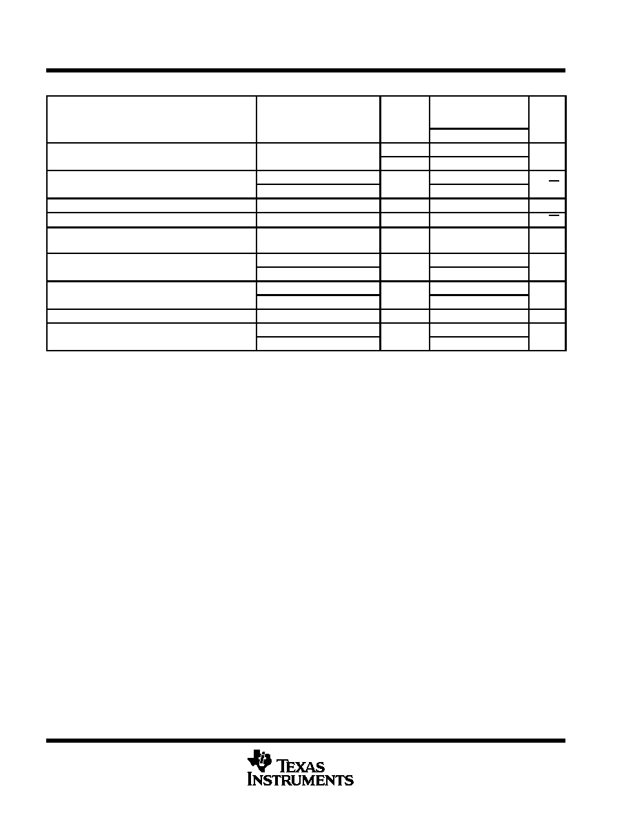
TLE2061Y electrical characteristics at V
CC
±
=
±
15 V, T
A
= 25
∞
C (unless otherwise noted)
PARAMETER
TEST CONDITIONS
TLE2061Y
UNIT
PARAMETER
TEST CONDITIONS
MIN
TYP
MAX
UNIT
VIO
Input offset voltage
0.6
3
mV
VIO
Input offset voltage long-term drift (see Note 4)
VIC = 0
RS = 50
0.04
µ
V/mo
IIO
Input offset current
VIC = 0,
RS = 50
2
pA
IIB
Input bias current
4
pA
VICR
Common-mode input voltage range
≠ 11
to
13
≠ 12
to
16
V
VOM
Maximum positive peak output voltage swing
RL = 10 k
13.2
13.7
V
VOM +
Maximum positive peak output voltage swing
RL = 600
12.5
13.2
V
VOM
Maximum negative peak output voltage swing
RL = 10 k
≠ 13.2
≠ 13.7
V
VOM ≠
Maximum negative peak output voltage swing
RL = 600
≠ 12.5
≠ 13
V
VO =
±
10 V,
RL = 10 k
30
230
AVD
Large-signal differential voltage amplification
VO = 0 to 8 V,
RL = 600
25
100
V/mV
VO = 0 to ≠ 8 V, RL = 600
3
25
ri
Input resistance
1012
ci
Input capacitance
4
pF
zo
Open-loop output impedance
IO = 0
280
CMRR
Common-mode rejection ratio
RS = 50
,
VIC = VICRmin
72
90
dB
kSVR
Supply voltage rejection ratio (
VCC /
VIO)
VCC
±
=
±
5 V to
±
15 V,
R
50
75
93
dB
kSVR
Supply-voltage rejection ratio (
VCC /
VIO)
RS = 50
75
93
dB
ICC
Supply current
VO = 0,
No load
290
350
µ
A
NOTE 4: Typical values are based on the input offset voltage shift observed through 168 hours of operating life test at TA = 150
∞
C extrapolated
to TA = 25
∞
C using the Arrhenius equation and assuming an activation energy of 0.96 eV.
TLE2061Y operating characteristics at V
CC
±
=
±
15 V, T
A
= 25
∞
C
PARAMETER
TEST CONDITIONS
TLE2061Y
UNIT
PARAMETER
TEST CONDITIONS
MIN
TYP
MAX
UNIT
SR
Slew rate at unity gain (see Figure 1)
RL = 10 k
,
CL = 100 pF
2.6
3.4
V/
µ
s
V
Equivalent input noise voltage (see Figure 2)
f = 10 Hz,
RS = 20
70
nV/
Hz
Vn
Equivalent input noise voltage (see Figure 2)
f = 1 kHz ,
RS = 20
40
nV/
Hz
VN(PP)
Peak-to-peak equivalent input noise voltage
f = 0.1 Hz to 10 Hz
1.1
µ
V
In
Equivalent input noise current
f = 1 Hz
1.1
fA /
Hz
THD
Total harmonic distortion
AVD
= 2,
f = 10 kHz,
0 025%
THD
Total harmonic distortion
VD
,
,
VO(PP) = 2 V,
RL = 10 k
0.025%
B1
Unity gain bandwidth (see Figure 3)
RL = 10 k
,
CL = 100 pF
2
MHz
B1
Unity-gain bandwidth (see Figure 3)
RL
= 600
,
CL = 100 pF
1.5
MHz
t
Settling time
0.1%
5
µ
s
ts
Settling time
0.01%
10
µ
s
BOM
Maximum output-swing bandwidth
AVD = 1,
RL
= 10 k
40
kHz
Phase margin at unity gain (see Figure 3)
RL
= 10 k
,
CL = 100 pF
60
∞
m
Phase margin at unity gain (see Figure 3)
RL
= 600
,
CL = 100 pF
70
∞
TLE206x, TLE206xA, TLE206xB, TLE206xY
EXCALIBUR JFET-INPUT HIGH-OUTPUT-DRIVE
µ
POWER OPERATIONAL AMPLIFIERS
SLOS193A ≠ FEBRUARY 1997 ≠ REVISED MARCH 1998
22
POST OFFICE BOX 655303
∑
DALLAS, TEXAS 75265
TLE2062C electrical characteristics at specified free-air temperature, V
CC
±
=
±
5 V (unless
otherwise noted)
PARAMETER
TEST CONDITIONS
TA
TLE2062C
TLE2062AC
TLE2062BC
UNIT
MIN
TYP
MAX
TLE2062C
25
∞
C
1
5
TLE2062C
Full range
5.9
VIO
Input offset voltage
TLE2062AC
25
∞
C
0.9
4
mV
VIO
Input offset voltage
TLE2062AC
Full range
4.9
mV
TLE2062BC
25
∞
C
0.7
3
TLE2062BC
VIC = 0
RS = 50
Full range
3.9
VIO
Temperature coefficient of input offset voltage
VIC = 0,
RS = 50
Full range
6
µ
V/
∞
C
Input offset voltage long-term drift (see Note 4)
25
∞
C
0.04
µ
V/mo
IIO
Input offset current
25
∞
C
1
pA
IIO
Input offset current
Full range
0.8
nA
IIB
Input bias current
25
∞
C
3
pA
IIB
Input bias current
Full range
2
nA
VICR
Common-mode input voltage range
25
∞
C
≠ 1.6
to
4
≠ 2
to
6
V
VICR
Common-mode in ut voltage range
Full range
≠ 1.6
to
4
V
RL = 10 k
25
∞
C
3.5
3.7
VOM
Maximum positive peak output voltage swing
RL = 10 k
Full range
3.3
V
VOM +
Maximum positive peak output voltage swing
RL = 100
25
∞
C
2.5
3.1
V
RL = 100
Full range
2
RL = 10 k
25
∞
C
≠ 3.7
≠ 3.9
VOM
Maximum negative peak output voltage swing
RL = 10 k
Full range
≠ 3.3
V
VOM ≠
Maximum negative peak output voltage swing
RL = 100
25
∞
C
≠ 2.5
≠ 2.7
V
RL = 100
Full range
≠ 2
VO =
±
2 8 V
RL = 10 k
25
∞
C
15
80
VO =
±
2.8 V,
RL = 10 k
Full range
2
AVD
Large signal differential voltage amplification
VO = 0 to 2 V
RL = 100
25
∞
C
0.75
45
V/mV
AVD
Large-signal differential voltage amplification
VO = 0 to 2 V,
RL = 100
Full range
0.5
V/mV
VO = 0 to 2 V
RL = 100
25
∞
C
0.5
3
VO = 0 to ≠ 2 V,
RL = 100
Full range
0.25
ri
Input resistance
25
∞
C
1012
ci
Input capacitance
25
∞
C
4
pF
zo
Open-loop output impedance
IO = 0
25
∞
C
560
CMRR
Common mode rejection ratio
VIC = VICRmin
RS = 50
25
∞
C
65
82
dB
CMRR
Common-mode rejection ratio
VIC = VICRmin, RS = 50
Full range
65
dB
kSVR
Supply voltage rejection ratio (
VCC
±
/
VIO)
VCC
±
=
±
5 V to
±
15 V,
25
∞
C
75
93
dB
kSVR
Supply-voltage rejection ratio (
VCC
±
/
VIO)
CC
±
RS = 50
Full range
75
dB
Full range is 0
∞
C to 70
∞
C.
NOTE 4: Typical values are based on the input offset voltage shift observed through 168 hours of operating life test at TA = 150
∞
C extrapolated
to TA = 25
∞
C using the Arrhenius equation and assuming an activation energy of 0.96 eV.
TLE206x, TLE206xA, TLE206xB, TLE206xY
EXCALIBUR JFET-INPUT HIGH-OUTPUT-DRIVE
µ
POWER OPERATIONAL AMPLIFIERS
SLOS193A ≠ FEBRUARY 1997 ≠ REVISED MARCH 1998
23
POST OFFICE BOX 655303
∑
DALLAS, TEXAS 75265
TLE2062C electrical characteristics at specified free-air temperature, V
CC
±
=
±
5 V (unless
otherwise noted) (continued)
PARAMETER
TEST CONDITIONS
TA
TLE2062C
TLE2062AC
TLE2062BC
UNIT
MIN
TYP
MAX
ICC
Supply current
25
∞
C
560
620
µ
A
ICC
Supply current
VO = 0
No load
Full range
635
µ
A
ICC
Supply-current change over operating
VO = 0,
No load
Full range
26
µ
A
ICC
y
g
g
temperature range
Full range
26
µ
A
Full range is 0
∞
C to 70
∞
C.
TLE2062C operating characteristics at specified free-air temperature, V
CC
±
=
±
5 V
PARAMETER
TEST CONDITIONS
TA
TLE2062C
TLE2062AC
TLE2062BC
UNIT
MIN
TYP
MAX
SR
Slew rate at unity gain (see Figure 1)
RL = 10 k
CL = 100 pF
25
∞
C
2.2
3.4
V/
µ
s
SR
Slew rate at unity gain (see Figure 1)
RL = 10 k
,
CL = 100 pF
Full range
2.1
V/
µ
s
V
Equivalent input noise voltage (see Figure 2)
f = 10 Hz,
RS = 20
25
∞
C
59
100
nV/
Hz
Vn
Equivalent input noise voltage (see Figure 2)
f = 1 kHz,
RS = 20
25
∞
C
43
60
nV/
Hz
VN(PP)
Peak-to-peak equivalent input noise voltage
f = 0.1 Hz to 10 Hz
25
∞
C
1.1
µ
V
In
Equivalent input noise current
f = 1 kHz
25
∞
C
1
fA/
Hz
THD
Total harmonic distortion
VO(PP) = 2 V,
RL = 10 k
,
25
∞
C
0 025%
THD
Total harmonic distortion
O(PP)
,
AVD = 2,
L
,
f = 10 kHz
25
∞
C
0.025%
B1
Unity gain bandwidth (see Figure 3)
RL = 10 k
,
CL = 100 pF
25
∞
C
1.8
MHz
B1
Unity-gain bandwidth (see Figure 3)
RL = 100
,
CL = 100 pF
25
∞
C
1.3
MHz
Settling time
0.1%
25
∞
C
5
µ
s
Settling time
0.01%
25
∞
C
10
µ
s
BOM
Maximum output-swing bandwidth
AVD = 1,
RL = 10 k
25
∞
C
140
kHz
Phase margin at unity gain (see Figure 3)
RL = 10 k
,
CL = 100 pF
25
∞
C
58
∞
m
Phase margin at unity gain (see Figure 3)
RL = 100
,
CL = 100 pF
25
∞
C
75
∞
Full range is 0
∞
C to 70
∞
C.
TLE206x, TLE206xA, TLE206xB, TLE206xY
EXCALIBUR JFET-INPUT HIGH-OUTPUT-DRIVE
µ
POWER OPERATIONAL AMPLIFIERS
SLOS193A ≠ FEBRUARY 1997 ≠ REVISED MARCH 1998
24
POST OFFICE BOX 655303
∑
DALLAS, TEXAS 75265
TLE2062C electrical characteristics at specified free-air temperature, V
CC
±
=
±
15 V (unless
otherwise noted)
PARAMETER
TEST CONDITIONS
TA
TLE2062C
TLE2062AC
TLE2062BC
UNIT
MIN
TYP
MAX
TLE2062C
25
∞
C
0.9
4
TLE2062C
Full range
4.9
VIO
Input offset voltage
TLE2062AC
25
∞
C
0.8
2
mV
VIO
Input offset voltage
TLE2062AC
Full range
2.9
mV
TLE2062BC
25
∞
C
0.5
1
TLE2062BC
VIC = 0
RS = 50
Full range
1.9
VIO
Temperature coefficient of input offset voltage
VIC = 0,
RS = 50
Full range
6
µ
V/
∞
C
Input offset voltage long-term drift (see Note 4)
25
∞
C
0.04
µ
V/mo
IIO
Input offset current
25
∞
C
2
pA
IIO
Input offset current
Full range
1
nA
IIB
Input bias current
25
∞
C
4
pA
IIB
Input bias current
Full range
3
nA
VICR
Common mode input voltage range
25
∞
C
≠ 11
to
13
≠ 12
to
16
V
VICR
Common-mode input voltage range
Full range
≠ 11
to
13
V
RL = 10 k
25
∞
C
13.2
13.7
VOM
Maximum positive peak output voltage swing
RL = 10 k
Full range
13
V
VOM + Maximum positive peak output voltage swing
RL = 600
25
∞
C
12.5
13.2
V
RL = 600
Full range
12
RL = 10 k
25
∞
C
≠ 13.2
≠ 13.7
VOM
Maximum negative peak output voltage swing
RL = 10 k
Full range
≠ 13
V
VOM ≠ Maximum negative peak output voltage swing
RL = 600
25
∞
C
≠ 12.5
≠ 13
V
RL = 600
Full range
≠ 12
VO =
±
10 V
RL = 10 k
25
∞
C
30
230
VO =
±
10 V,
RL = 10 k
Full range
20
AVD
Large signal differential voltage amplification
VO = 0 to 8 V
RL = 600
25
∞
C
25
100
V/mV
AVD
Large-signal differential voltage amplification
VO = 0 to 8 V,
RL = 600
Full range
10
V/mV
VO = 0 to 8 V
RL = 600
25
∞
C
3
25
VO = 0 to ≠ 8 V,
RL = 600
Full range
1
ri
Input resistance
25
∞
C
1012
ci
Input capacitance
25
∞
C
4
pF
zo
Open-loop output impedance
IO = 0
25
∞
C
560
CMRR
Common mode rejection ratio
VIC = VICRmin
RS = 50
25
∞
C
72
90
dB
CMRR
Common-mode rejection ratio
VIC = VICRmin, RS = 50
Full range
70
dB
kSVR
Supply voltage rejection ratio (
VCC
±
/
VIO)
VCC
±
=
±
5 V to
±
15 V,
25
∞
C
75
93
dB
kSVR
Supply-voltage rejection ratio (
VCC
±
/
VIO)
CC
±
RS = 50
Full range
75
dB
Full range is 0
∞
C to 70
∞
C.
NOTE 4: Typical values are based on the input offset voltage shift observed through 168 hours of operating life test at TA = 150
∞
C extrapolated
to TA = 25
∞
C using the Arrhenius equation and assuming an activation energy of 0.96 eV.
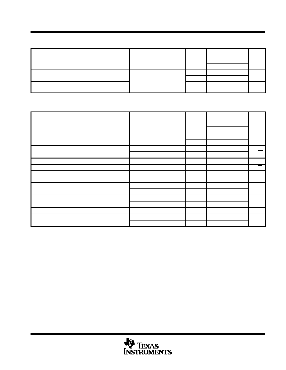
TLE206x, TLE206xA, TLE206xB, TLE206xY
EXCALIBUR JFET-INPUT HIGH-OUTPUT-DRIVE
µ
POWER OPERATIONAL AMPLIFIERS
SLOS193A ≠ FEBRUARY 1997 ≠ REVISED MARCH 1998
25
POST OFFICE BOX 655303
∑
DALLAS, TEXAS 75265
TLE2062C electrical characteristics at specified free-air temperature, V
CC
±
=
±
15 V (unless
otherwise noted) (continued)
PARAMETER
TEST CONDITIONS
TA
TLE2062C
TLE2062AC
TLE2062BC
UNIT
MIN
TYP
MAX
ICC
Supply current
25
∞
C
625
690
µ
A
ICC
Supply current
VO = 0 V
No load
Full range
715
µ
A
ICC
Supply-current change over operating
VO = 0 V,
No load
Full range
36
µ
A
ICC
y
g
g
temperature range
Full range
36
µ
A
Full range is 0
∞
C to 70
∞
C.
TLE2062C operating characteristics at specified free-air temperature, V
CC
±
=
±
15 V
PARAMETER
TEST CONDITIONS
TA
TLE2062C
TLE2062AC
TLE2062BC
UNIT
MIN
TYP
MAX
SR
Slew rate at unity gain (see Figure 1)
RL = 10 k
CL = 100 pF
25
∞
C
2.6
3.4
V/
µ
s
SR
Slew rate at unity gain (see Figure 1)
RL = 10 k
,
CL = 100 pF
Full range
2.5
V/
µ
s
V
Equivalent input noise voltage (see Figure 2)
f = 10 Hz,
RS = 20
25
∞
C
70
100
V/
H
Vn
Equivalent input noise voltage (see Figure 2)
f = 1 kHz,
RS = 20
25
∞
C
40
60
nV/
Hz
VN(PP)
Peak-to-peak equivalent input noise voltage
f = 0.1 Hz to 10 Hz
25
∞
C
1.1
µ
V
In
Equivalent input noise current
f = 1 kHz
25
∞
C
1.1
fA/
Hz
THD
Total harmonic distortion
VO(PP) = 2 V,
RL = 10 k
,
25
∞
C
0 025%
THD
Total harmonic distortion
O(PP)
,
AVD = 2,
L
,
f = 10 kHz
25
∞
C
0.025%
B1
Unity gain bandwidth (see Figure 3)
RL = 10 k
,
CL = 10 0 pF
25
∞
C
2
MHz
B1
Unity-gain bandwidth (see Figure 3)
RL = 600
,
CL = 100 pF
25
∞
C
1.5
MHz
Settling time
0.1%
25
∞
C
5
µ
s
Settling time
0.01%
25
∞
C
10
µ
s
BOM
Maximum output-swing bandwidth
AVD = 1,
RL = 10 k
25
∞
C
40
kHz
Phase margin at unity gain (see Figure 3)
RL = 10 k
,
CL = 100 pF
25
∞
C
60
∞
m
Phase margin at unity gain (see Figure 3)
RL = 600
,
CL = 100 pF
25
∞
C
70
∞
Full range is 0
∞
C to 70
∞
C.
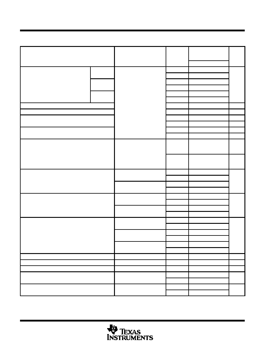
TLE206x, TLE206xA, TLE206xB, TLE206xY
EXCALIBUR JFET-INPUT HIGH-OUTPUT-DRIVE
µ
POWER OPERATIONAL AMPLIFIERS
SLOS193A ≠ FEBRUARY 1997 ≠ REVISED MARCH 1998
26
POST OFFICE BOX 655303
∑
DALLAS, TEXAS 75265
TLE2062I electrical characteristics at specified free-air temperature, V
CC
±
=
±
5 V (unless otherwise
noted)
PARAMETER
TEST CONDITIONS
TA
TLE2062I
TLE2062AI
TLE2062BI
UNIT
MIN
TYP
MAX
TLE2062I
25
∞
C
1
5
TLE2062I
Full range
6.3
VIO
Input offset voltage
TLE2062AI
25
∞
C
0.9
4
mV
VIO
Input offset voltage
TLE2062AI
Full range
5.3
mV
TLE2062BI
25
∞
C
0.7
3
TLE2062BI
VIC = 0
RS = 50
Full range
4.3
VIO
Temperature coefficient of input offset voltage
VIC = 0,
RS = 50
Full range
6
µ
V/
∞
C
Input offset voltage long-term drift (see Note 4)
25
∞
C
0.04
µ
V/mo
IIO
Input offset current
25
∞
C
1
pA
IIO
Input offset current
Full range
2
nA
IIB
Input bias current
25
∞
C
3
pA
IIB
Input bias current
Full range
4
nA
VICR
Common mode input voltage range
25
∞
C
≠ 1.6
to
4
≠ 2
to
6
V
VICR
Common-mode input voltage range
Full range
≠ 1.6
to
4
V
RL = 10 k
25
∞
C
3.5
3.7
VOM
Maximum positive peak output voltage swing
RL = 10 k
Full range
3.1
V
VOM +
Maximum positive peak output voltage swing
RL = 100
25
∞
C
2.5
3.1
V
RL = 100
Full range
2
RL = 10 k
25
∞
C
≠ 3.7
≠ 3.9
VOM
Maximum negative peak output voltage swing
RL = 10 k
Full range
≠ 3.1
V
VOM ≠
Maximum negative peak output voltage swing
RL = 100
25
∞
C
≠ 2.5
≠ 2.7
V
RL = 100
Full range
≠ 2
VO =
±
2 8 V
RL = 10 k
25
∞
C
15
80
VO =
±
2.8 V,
RL = 10 k
Full range
2
AVD
Large signal differential voltage amplification
VO = 0 to 2 V
RL = 100
25
∞
C
0.75
45
V/mV
AVD
Large-signal differential voltage amplification
VO = 0 to 2 V,
RL = 100
Full range
0.5
V/mV
VO = 0 to 2 V
RL = 100
25
∞
C
0.5
3
VO = 0 to ≠ 2 V,
RL = 100
Full range
0.25
ri
Input resistance
25
∞
C
1012
ci
Input capacitance
25
∞
C
4
pF
zo
Open-loop output impedance
IO = 0
25
∞
C
560
CMRR
Common mode rejection ratio
VIC = VICRmin
RS = 50
25
∞
C
65
82
dB
CMRR
Common-mode rejection ratio
VIC = VICRmin, RS = 50
Full range
65
dB
kSVR
Supply voltage rejection ratio (
VCC
±
/
VIO)
VCC
±
=
±
5 V to
±
15 V,
25
∞
C
75
93
dB
kSVR
Supply-voltage rejection ratio (
VCC
±
/
VIO)
CC
±
RS = 50
Full range
65
dB
Full range is ≠ 40
∞
C to 85
∞
C.
NOTE 4: Typical values are based on the input offset voltage shift observed through 168 hours of operating life test at TA = 150
∞
C extrapolated
to TA = 25
∞
C using the Arrhenius equation and assuming an activation energy of 0.96 eV.

TLE206x, TLE206xA, TLE206xB, TLE206xY
EXCALIBUR JFET-INPUT HIGH-OUTPUT-DRIVE
µ
POWER OPERATIONAL AMPLIFIERS
SLOS193A ≠ FEBRUARY 1997 ≠ REVISED MARCH 1998
27
POST OFFICE BOX 655303
∑
DALLAS, TEXAS 75265
TLE2062I electrical characteristics at specified free-air temperature, V
CC
±
=
±
5 V (unless otherwise
noted) (continued)
PARAMETER
TEST CONDITIONS
TA
TLE2062I
TLE2062AI
TLE2062BI
UNIT
MIN
TYP
MAX
ICC
Supply current
25
∞
C
560
620
µ
A
ICC
Supply current
VO = 0
No load
Full range
640
µ
A
ICC
Supply-current change over operating
VO = 0,
No load
Full range
54
µ
A
ICC
y
g
g
temperature range
Full range
54
µ
A
Full range is ≠ 40
∞
C to 85
∞
C.
TLE2062I operating characteristics at specified free-air temperature, V
CC
±
=
±
5 V
PARAMETER
TEST CONDITIONS
TA
TLE2062I
TLE2062AI
TLE2062BI
UNIT
MIN
TYP
MAX
SR
Slew rate at unity gain (see Figure 1)
RL = 10 k
CL = 100 pF
25
∞
C
2.2
3.4
V/
µ
s
SR
Slew rate at unity gain (see Figure 1)
RL = 10 k
,
CL = 100 pF
Full range
1.7
V/
µ
s
V
Equivalent input noise voltage (see Figure 2)
f = 10 Hz,
RS = 20
25
∞
C
59
100
nV/
Hz
Vn
Equivalent input noise voltage (see Figure 2)
f = 1 kHz,
RS = 20
25
∞
C
43
60
nV/
Hz
VN(PP)
Peak-to-peak equivalent input noise voltage
f = 0.1 Hz to 10 Hz
25
∞
C
1.1
µ
V
In
Equivalent input noise current
f = 1 kHz
25
∞
C
1
fA/
Hz
THD
Total harmonic distortion
VO(PP) = 2 V,
RL = 10 k
,
25
∞
C
0 025%
THD
Total harmonic distortion
O(PP)
,
AVD = 2,
L
,
f = 10 kHz
25
∞
C
0.025%
B1
Unity gain bandwidth (see Figure 3)
RL = 10 k
,
CL = 100 pF
25
∞
C
1.8
MHz
B1
Unity-gain bandwidth (see Figure 3)
RL = 100
,
CL = 100 pF
25
∞
C
1.3
MHz
Settling time
0.1%
25
∞
C
5
µ
s
Settling time
0.01%
25
∞
C
10
µ
s
BOM
Maximum output-swing bandwidth
AVD = 1,
RL = 10 k
25
∞
C
140
kHz
Phase margin at unity gain (see Figure 3)
RL = 10 k
,
CL = 100 pF
25
∞
C
58
∞
m
Phase margin at unity gain (see Figure 3)
RL = 100
,
CL = 100 pF
25
∞
C
75
∞
Full range is ≠ 40
∞
C to 85
∞
C.

TLE206x, TLE206xA, TLE206xB, TLE206xY
EXCALIBUR JFET-INPUT HIGH-OUTPUT-DRIVE
µ
POWER OPERATIONAL AMPLIFIERS
SLOS193A ≠ FEBRUARY 1997 ≠ REVISED MARCH 1998
28
POST OFFICE BOX 655303
∑
DALLAS, TEXAS 75265
TLE2062I electrical characteristics at specified free-air temperature, V
CC
±
=
±
15 V (unless
otherwise noted)
PARAMETER
TEST CONDITIONS
TA
TLE2062I
TLE2062AI
TLE2062BI
UNIT
MIN
TYP
MAX
TLE2062I
25
∞
C
0.9
4
TLE2062I
Full range
5.3
VIO
Input offset voltage
TLE2062AI
25
∞
C
0.8
2
mV
VIO
Input offset voltage
TLE2062AI
Full range
3.3
mV
TLE2062BI
25
∞
C
0.5
1
TLE2062BI
VIC = 0
RS = 50
Full range
2.3
VIO
Temperature coefficient of input offset voltage
VIC = 0,
RS = 50
Full range
6
µ
V/
∞
C
Input offset voltage long-term drift (see Note 4)
25
∞
C
0.04
µ
V/mo
IIO
Input offset current
25
∞
C
2
pA
IIO
Input offset current
Full range
3
nA
IIB
Input bias current
25
∞
C
4
pA
IIB
Input bias current
Full range
5
nA
VICR
Common mode input voltage range
25
∞
C
≠ 11
to
13
≠ 12
to
16
V
VICR
Common-mode input voltage range
Full range
≠ 11
to
13
V
RL = 10 k
25
∞
C
13.2
13.7
VOM
Maximum positive peak output voltage swing
RL = 10 k
Full range
13
V
VOM +
Maximum positive peak output voltage swing
RL = 600
25
∞
C
12.5
13.2
V
RL = 600
Full range
12
RL = 10 k
25
∞
C
≠ 13.2
≠ 13.7
VOM
Maximum negative peak output voltage swing
RL = 10 k
Full range
≠ 13
V
VOM ≠
Maximum negative peak output voltage swing
RL = 600
25
∞
C
≠ 12.5
≠ 13
V
RL = 600
Full range
≠ 12
VO =
±
10 V
RL = 10 k
25
∞
C
30
230
VO =
±
10 V,
RL = 10 k
Full range
20
AVD
Large signal differential voltage amplification
VO = 0 to 8 V
RL = 600
25
∞
C
25
100
V/mV
AVD
Large-signal differential voltage amplification
VO = 0 to 8 V,
RL = 600
Full range
10
V/mV
VO = 0 to 8 V
RL = 600
25
∞
C
3
25
VO = 0 to ≠ 8 V,
RL = 600
Full range
1
ri
Input resistance
25
∞
C
1012
ci
Input capacitance
25
∞
C
4
pF
zo
Open-loop output impedance
IO = 0
25
∞
C
560
CMRR
Common mode rejection ratio
VIC = VICRmin
RS = 50
25
∞
C
72
90
dB
CMRR
Common-mode rejection ratio
VIC = VICRmin, RS = 50
Full range
65
dB
kSVR
Supply voltage rejection ratio (
VCC
±
/
VIO)
VCC
±
=
±
5 V to
±
15 V,
25
∞
C
75
93
dB
kSVR
Supply-voltage rejection ratio (
VCC
±
/
VIO)
CC
±
RS = 50
Full range
65
dB
Full range is ≠ 40
∞
C to 85
∞
C.
NOTE 4: Typical values are based on the input offset voltage shift observed through 168 hours of operating life test at TA = 150
∞
C extrapolated
to TA = 25
∞
C using the Arrhenius equation and assuming an activation energy of 0.96 eV.

TLE206x, TLE206xA, TLE206xB, TLE206xY
EXCALIBUR JFET-INPUT HIGH-OUTPUT-DRIVE
µ
POWER OPERATIONAL AMPLIFIERS
SLOS193A ≠ FEBRUARY 1997 ≠ REVISED MARCH 1998
29
POST OFFICE BOX 655303
∑
DALLAS, TEXAS 75265
TLE2062I electrical characteristics at specified free-air temperature, V
CC
±
=
±
15 V (unless
otherwise noted) (continued)
PARAMETER
TEST CONDITIONS
TA
TLE2062I
TLE2062AI
TLE2062BI
UNIT
MIN
TYP
MAX
ICC
Supply current
25
∞
C
625
690
µ
A
ICC
Supply current
VO = 0
No load
Full range
720
µ
A
ICC
Supply-current change over operating
VO = 0,
No load
Full range
74
µ
A
ICC
y
g
g
temperature range
Full range
74
µ
A
Full range is ≠ 40
∞
C to 85
∞
C.
TLE2062I operating characteristics at specified free-air temperature, V
CC
±
=
±
15 V
PARAMETER
TEST CONDITIONS
TA
TLE2062I
TLE2062AI
TLE2062BI
UNIT
MIN
TYP
MAX
SR
Slew rate at unity gain (see Figure 1)
RL = 10 k
CL = 100 pF
25
∞
C
2.6
3.4
V/
µ
s
SR
Slew rate at unity gain (see Figure 1)
RL = 10 k
,
CL = 100 pF
Full range
2.1
V/
µ
s
V
Equivalent input noise voltage (see Figure 2)
f = 10 Hz,
RS = 20
25
∞
C
70
100
nV/
Hz
Vn
Equivalent input noise voltage (see Figure 2)
f = 1 kHz,
RS = 20
25
∞
C
40
60
nV/
Hz
VN(PP)
Peak-to-peak equivalent input noise voltage
f = 0.1 Hz to 10 Hz
25
∞
C
1.1
µ
V
In
Equivalent input noise current
f = 1 kHz
25
∞
C
1.1
fA/
Hz
THD
Total harmonic distortion
VO(PP) = 2 V,
RL = 10 k
,
25
∞
C
0 025%
THD
Total harmonic distortion
O(PP)
,
AVD = 2,
L
,
f = 10 kHz
25
∞
C
0.025%
B1
Unity gain bandwidth (see Figure 3)
RL = 10 k
,
CL = 100 pF
25
∞
C
2
MHz
B1
Unity-gain bandwidth (see Figure 3)
RL = 600
,
CL = 100 pF
25
∞
C
1.5
MHz
Settling time
0.1%
25
∞
C
5
µ
s
Settling time
0.01%
25
∞
C
10
µ
s
BOM
Maximum output-swing bandwidth
AVD = 1,
RL = 10 k
25
∞
C
40
kHz
Phase margin at unity gain (see Figure 3)
RL = 10 k
,
CL = 100 pF
25
∞
C
60
∞
m
Phase margin at unity gain (see Figure 3)
RL = 600
,
CL = 100 pF
25
∞
C
70
∞
Full range is ≠ 40
∞
C to 85
∞
C.
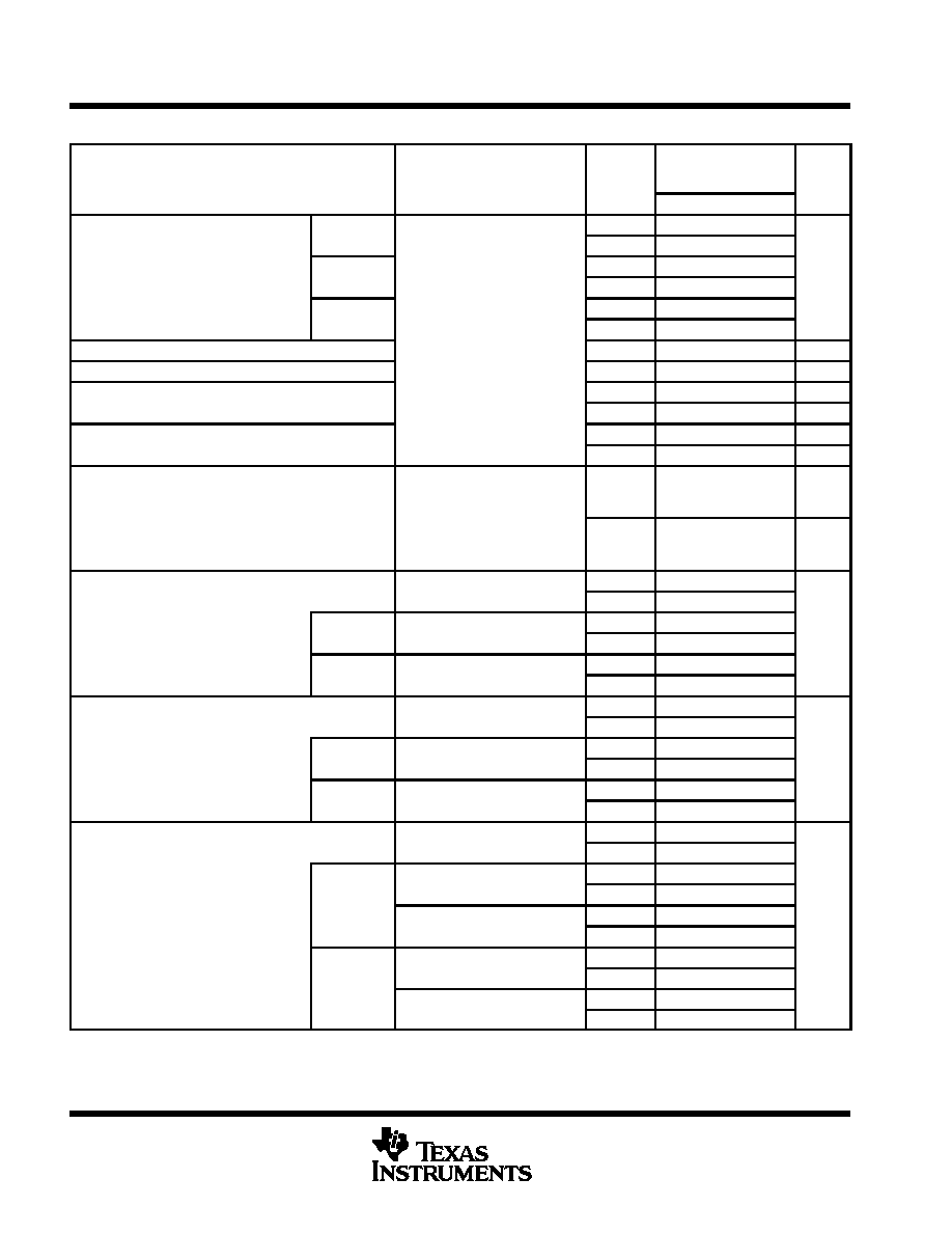
TLE206x, TLE206xA, TLE206xB, TLE206xY
EXCALIBUR JFET-INPUT HIGH-OUTPUT-DRIVE
µ
POWER OPERATIONAL AMPLIFIERS
SLOS193A ≠ FEBRUARY 1997 ≠ REVISED MARCH 1998
30
POST OFFICE BOX 655303
∑
DALLAS, TEXAS 75265
TLE2062M electrical characteristics at specified free-air temperature, V
CC
±
=
±
5 V
PARAMETER
TEST CONDITIONS
TA
TLE2062M
TLE2062AM
TLE2062BM
UNIT
MIN
TYP
MAX
TLE2062M
25
∞
C
1
5
TLE2062M
Full range
7
VIO
Input offset voltage
TLE2062AM
25
∞
C
0.9
4
mV
VIO
Input offset voltage
TLE2062AM
Full range
6
mV
TLE2062BM
25
∞
C
0.7
3
TLE2062BM
VIC = 0
RS = 50
Full range
5
VIO
Temperature coefficient of input offset voltage
VIC = 0,
RS = 50
Full range
6
µ
V/
∞
C
Input offset voltage long-term drift (see Note 4)
25
∞
C
0.04
µ
V/mo
IIO
Input offset current
25
∞
C
1
pA
IIO
Input offset current
Full range
15
nA
IIB
Input bias current
25
∞
C
3
pA
IIB
Input bias current
Full range
30
nA
VICR
Common mode input voltage range
25
∞
C
≠ 1.6
to
4
≠ 2
to
6
V
VICR
Common-mode input voltage range
Full range
≠ 1.6
to
4
V
RL = 10 k
25
∞
C
3.5
3.7
RL = 10 k
Full range
3
VOM
Maximum positive peak output
FK and JG
RL = 600
25
∞
C
2.5
3.6
V
VOM +
voltage swing
FK and JG
packages
RL = 600
Full range
2
V
D and P
RL = 100
25
∞
C
2.5
3.1
D and P
packages
RL = 100
Full range
2
RL = 10 k
25
∞
C
≠ 3.5
≠ 3.9
RL = 10 k
Full range
≠ 3
VOM
Maximum negative peak output
FK and JG
RL = 600
25
∞
C
≠ 2.5
≠ 3.5
V
VOM ≠
g
voltage swing
FK and JG
packages
RL = 600
Full range
≠ 2
V
D and P
RL = 100
25
∞
C
≠ 2.5
≠ 2.7
D and P
packages
RL = 100
Full range
≠ 2
VO =
±
2 8 V
RL = 10 k
25
∞
C
15
80
VO =
±
2.8 V,
RL = 10 k
Full range
2
VO = 0 to 2 5 V
RL = 600
25
∞
C
1
65
FK and JG
VO = 0 to 2.5 V,
RL = 600
Full range
0.5
AVD
Large-signal differential voltage
FK and JG
packages
VO = 0 to 2 5 V
RL = 600
25
∞
C
1
16
V/mV
AVD
g
g
g
amplification
VO = 0 to ≠ 2.5 V,
RL = 600
Full range
0.5
V/mV
VO = 0 to 2 V
RL = 100
25
∞
C
0.75
45
D and P
VO = 0 to 2 V,
RL = 100
Full range
0.5
D and P
packages
VO = 0 to 2 V
RL = 100
25
∞
C
0.5
3
VO = 0 to ≠ 2 V,
RL = 100
Full range
0.25
Full range is ≠ 55
∞
C to 125
∞
C.
NOTE 4: Typical values are based on the input offset voltage shift observed through 168 hours of operating life test at TA = 150
∞
C extrapolated
to TA = 25
∞
C using the Arrhenius equation and assuming an activation energy of 0.96 eV.
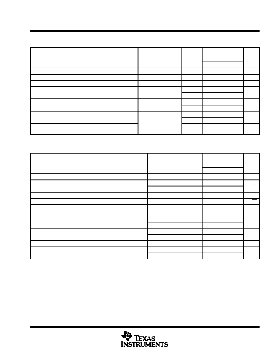
TLE206x, TLE206xA, TLE206xB, TLE206xY
EXCALIBUR JFET-INPUT HIGH-OUTPUT-DRIVE
µ
POWER OPERATIONAL AMPLIFIERS
SLOS193A ≠ FEBRUARY 1997 ≠ REVISED MARCH 1998
31
POST OFFICE BOX 655303
∑
DALLAS, TEXAS 75265
TLE2062M electrical characteristics at specified free-air temperature, V
CC
±
=
±
5 V (unless
otherwise noted)
PARAMETER
TEST CONDITIONS
TA
TLE2062M
TLE2062AM
TLE2062BM
UNIT
MIN
TYP
MAX
ri
Input resistance
25
∞
C
1012
ci
Input capacitance
25
∞
C
4
pF
zo
Open-loop output impedance
IO = 0
25
∞
C
560
CMRR
Common mode rejection ratio
VIC = VICRmin
25
∞
C
65
82
dB
CMRR
Common-mode rejection ratio
RS = 50
,
Full range
60
dB
kSVR
Supply voltage rejection ratio (
VCC
±
/
VIO)
VCC
±
=
±
5 V to
±
15 V,
25
∞
C
75
93
dB
kSVR
Supply-voltage rejection ratio (
VCC
±
/
VIO)
RS = 50
Full range
65
dB
ICC
Supply current (two amplifiers)
25
∞
C
560
620
µ
A
ICC
Supply current (two amplifiers)
VO = 0
No load
Full range
650
µ
A
ICC
Supply-current change over operating
VO = 0,
No load
Full range
72
µ
A
ICC
y
g
g
temperature range (two amplifiers)
Full range
72
µ
A
Full range is ≠ 55
∞
C to 125
∞
C.
TLE2062M operating characteristics at specified free-air temperature, T
A
= 25
∞
C, V
CC
±
=
±
5 V
PARAMETER
TEST CONDITIONS
TLE2062M
TLE2062AM
TLE2062BM
UNIT
MIN
TYP
MAX
SR
Slew rate at unity gain (see Figure 1)
RL = 10 k
,
CL = 100 pF
3.4
V/
µ
s
V
Equivalent input noise voltage (see Figure 2)
f = 10 Hz,
RS = 20
59
nV/
Hz
Vn
Equivalent input noise voltage (see Figure 2)
f = 1 kHz,
RS = 20
43
nV/
Hz
VN(PP)
Peak-to-peak equivalent input noise voltage
f = 0.1 Hz to 10 Hz
1.1
µ
V
In
Equivalent input noise current
f = 1 kHz
1
fA/
Hz
THD
Total harmonic distortion
VO(PP) = 2 V,
RL = 10 k
,
0 025%
THD
Total harmonic distortion
O(PP)
,
AVD = 2,
L
,
f = 10 kHz
0.025%
B1
Unity gain bandwidth (see Figure 3)
RL = 10 k
,
CL = 100 pF
1.8
MHz
B1
Unity-gain bandwidth (see Figure 3)
RL = 600
,
CL = 100 pF
1.3
MHz
Settling time
0.1%
5
µ
s
Settling time
0.01%
10
µ
s
BOM
Maximum output-swing bandwidth
AVD = 1,
RL = 10 k
140
kHz
Phase margin at unity gain (see Figure 3)
RL = 10 k
,
CL = 100 pF
58
∞
m
Phase margin at unity gain (see Figure 3)
RL = 600
,
CL = 100 pF
75
∞
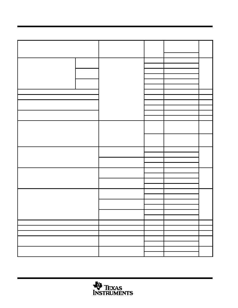
TLE206x, TLE206xA, TLE206xB, TLE206xY
EXCALIBUR JFET-INPUT HIGH-OUTPUT-DRIVE
µ
POWER OPERATIONAL AMPLIFIERS
SLOS193A ≠ FEBRUARY 1997 ≠ REVISED MARCH 1998
32
POST OFFICE BOX 655303
∑
DALLAS, TEXAS 75265
TLE2062M electrical characteristics at specified free-air temperature, V
CC
±
=
±
15 V (unless
otherwise noted)
PARAMETER
TEST CONDITIONS
TA
TLE2062M
TLE2062AM
TLE2062BM
UNIT
MIN
TYP
MAX
TLE2062M
25
∞
C
0.9
4
TLE2062M
Full range
6
VIO
Input offset voltage
TLE2062AM
25
∞
C
0.8
2
mV
VIO
Input offset voltage
TLE2062AM
Full range
4
mV
TLE2062BM
25
∞
C
0.5
1
TLE2062BM
VIC = 0
RS = 50
Full range
3
VIO
Temperature coefficient of input offset voltage
VIC = 0,
RS = 50
Full range
6
µ
V/
∞
C
Input offset voltage long-term drift (see Note 4)
25
∞
C
0.04
µ
V/mo
IIO
Input offset current
25
∞
C
2
pA
IIO
Input offset current
Full range
20
nA
IIB
Input bias current
25
∞
C
4
pA
IIB
Input bias current
Full range
40
nA
VICR
Common mode input voltage range
25
∞
C
≠ 11
to
13
≠ 12
to
16
V
VICR
Common-mode input voltage range
Full range
≠ 11
to
13
V
RL = 10 k
25
∞
C
13
13.7
VOM
Maximum positive peak output voltage swing
RL = 10 k
Full range
12.5
V
VOM +
Maximum positive peak output voltage swing
RL = 600
25
∞
C
12.5
13.2
V
RL = 600
Full range
11
RL = 10 k
25
∞
C
≠ 13
≠ 13.7
VOM
Maximum negative peak output voltage swing
RL = 10 k
Full range
≠ 12.5
V
VOM ≠
Maximum negative peak output voltage swing
RL = 600
25
∞
C
≠ 12.5
≠ 13
V
RL = 600
Full range
≠ 11
VO =
±
10 V
RL = 10 k
25
∞
C
30
230
VO =
±
10 V,
RL = 10 k
Full range
20
AVD
Large signal differential voltage amplification
VO = 0 to 8 V
RL = 600
25
∞
C
25
100
V/mV
AVD
Large-signal differential voltage amplification
VO = 0 to 8 V,
RL = 600
Full range
7
V/mV
VO = 0 to 8 V
RL = 600
25
∞
C
3
25
VO = 0 to ≠ 8 V,
RL = 600
Full range
1
ri
Input resistance
25
∞
C
1012
ci
Input capacitance
25
∞
C
4
pF
zo
Open-loop output impedance
IO = 0
25
∞
C
560
CMRR
Common mode rejection ratio
VIC = VICRmin
RS = 50
25
∞
C
72
90
dB
CMRR
Common-mode rejection ratio
VIC = VICRmin, RS = 50
Full range
65
dB
kSVR
Supply voltage rejection ratio (
VCC
±
/
VIO)
VCC
±
=
±
5 V to
±
15 V,
25
∞
C
75
93
dB
kSVR
Supply-voltage rejection ratio (
VCC
±
/
VIO)
CC
±
RS = 50
Full range
65
dB
Full range is ≠ 55
∞
C to 125
∞
C.
NOTE 4: Typical values are based on the input offset voltage shift observed through 168 hours of operating life test at TA = 150
∞
C extrapolated
to TA = 25
∞
C using the Arrhenius equation and assuming an activation energy of 0.96 eV.
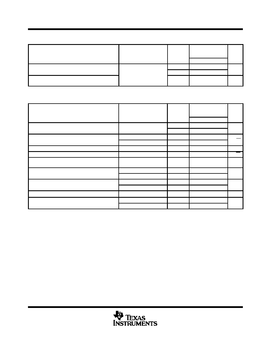
TLE206x, TLE206xA, TLE206xB, TLE206xY
EXCALIBUR JFET-INPUT HIGH-OUTPUT-DRIVE
µ
POWER OPERATIONAL AMPLIFIERS
SLOS193A ≠ FEBRUARY 1997 ≠ REVISED MARCH 1998
33
POST OFFICE BOX 655303
∑
DALLAS, TEXAS 75265
TLE2062M electrical characteristics at specified free-air temperature, V
CC
±
=
±
15 V (unless
otherwise noted)
PARAMETER
TEST CONDITIONS
TA
TLE2062M
TLE2062AM
TLE2062BM
UNIT
MIN
TYP
MAX
ICC
Supply current
25
∞
C
625
690
µ
A
ICC
Supply current
VO = 0
No load
Full range
730
µ
A
ICC
Supply-current change over operating
VO = 0,
No load
Full range
97
µ
A
ICC
y
g
g
temperature range
Full range
97
µ
A
Full range is ≠ 55
∞
C to 125
∞
C.
TLE2062M operating characteristics at specified free-air temperature, V
CC
±
=
±
15 V
PARAMETER
TEST CONDITIONS
TA
TLE2062M
TLE2062AM
TLE2062BM
UNIT
MIN
TYP
MAX
SR
Slew rate at unity gain (see Figure 1)
RL = 10 k
CL = 100 pF
25
∞
C
2
3.4
V/
µ
s
SR
Slew rate at unity gain (see Figure 1)
RL = 10 k
,
CL = 100 pF
Full range
1.8
V/
µ
s
V
Equivalent input noise voltage (see Figure 2)
f = 10 Hz,
RS = 20
25
∞
C
70
nV/
Hz
Vn
Equivalent input noise voltage (see Figure 2)
f = 1 kHz,
RS = 20
25
∞
C
40
nV/
Hz
VN(PP)
Peak-to-peak equivalent input noise voltage
f = 0.1 Hz to 10 Hz
25
∞
C
1.1
µ
V
In
Equivalent input noise current
f = 1 kHz
25
∞
C
1.1
fA/
Hz
THD
Total harmonic distortion
VO(PP) = 2 V,
AVD = 2,
RL = 10 k
,
f = 10 kHz
25
∞
C
0.025%
B1
Unity gain bandwidth (see Figure 3)
RL = 10 k
,
CL = 100 pF
25
∞
C
2
MHz
B1
Unity-gain bandwidth (see Figure 3)
RL = 600
,
CL = 100 pF
25
∞
C
1.5
MHz
Settling time
0.1%
25
∞
C
5
µ
s
Settling time
0.01%
25
∞
C
10
µ
s
BOM
Maximum output swing bandwidth
AVD = 1
RL = 10 k
25
∞
C
40
kHz
BOM
Maximum output-swing bandwidth
AVD = 1,
RL = 10 k
25
∞
C
40
kHz
Phase margin at unity gain (see Figure 3)
RL = 10 k
,
CL = 100 pF
25
∞
C
60
∞
m
Phase margin at unity gain (see Figure 3)
RL = 600
,
CL = 100 pF
25
∞
C
70
∞
Full range is ≠ 55
∞
C to 125
∞
C.
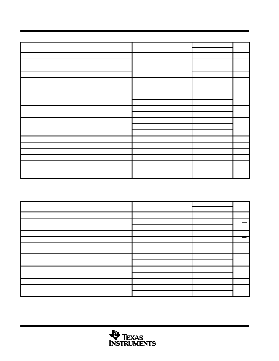
TLE206x, TLE206xA, TLE206xB, TLE206xY
EXCALIBUR JFET-INPUT HIGH-OUTPUT-DRIVE
µ
POWER OPERATIONAL AMPLIFIERS
SLOS193A ≠ FEBRUARY 1997 ≠ REVISED MARCH 1998
34
POST OFFICE BOX 655303
∑
DALLAS, TEXAS 75265
TLE2062Y electrical characteristics at V
CC
±
=
±
15 V, T
A
= 25
∞
C (unless otherwise noted)
PARAMETER
TEST CONDITIONS
TLE2062Y
UNIT
PARAMETER
TEST CONDITIONS
MIN
TYP
MAX
UNIT
VIO
Input offset voltage
0.9
4
mV
VIO
Input offset voltage long-term drift (see Note 4)
VIC = 0
RS = 50
0.04
µ
V/mo
IIO
Input offset current
VIC = 0,
RS = 50
2
pA
IIB
Input bias current
4
pA
≠ 11
≠ 12
VICR
Common-mode input voltage range
11
to
12
to
V
ICR
g
g
13
16
VOM
Maximum positive peak output voltage swing
RL = 10 k
13.2
13.7
V
VOM +
Maximum positive peak output voltage swing
RL = 600
12.5
13.2
V
VOM
Maximum negative peak output voltage swing
RL = 10 k
≠ 13.2
≠ 13.7
V
VOM ≠
Maximum negative peak output voltage swing
RL = 600
≠ 12.5
≠ 13
V
VO =
±
10 V,
RL = 10 k
30
230
AVD
Large-signal differential voltage amplification
VO = 0 to 8 V,
RL = 600
25
100
V/mV
VO = 0 to ≠ 8 V,
RL = 600
3
25
ri
Input resistance
1012
ci
Input capacitance
4
pF
zo
Open-loop output impedance
IO = 0
560
CMRR
Common-mode rejection ratio
VIC = VICRmin,
RS = 50
72
90
dB
kSVR
Supply voltage rejection ratio (
VCC /
VIO)
VCC
±
=
±
5 V to
±
15 V,
75
93
dB
kSVR
Supply-voltage rejection ratio (
VCC /
VIO)
CC
±
,
RS = 50
75
93
dB
ICC
Supply current
VO = 0,
No load
625
690
µ
A
NOTE 4: Typical values are based on the input offset voltage shift observed through 168 hours of operating life test at TA = 150
∞
C extrapolated
to TA = 25
∞
C using the Arrhenius equation and assuming an activation energy of 0.96 eV.
TLE2062Y operating characteristics at V
CC
±
=
±
15 V, T
A
= 25
∞
C
PARAMETER
TEST CONDITIONS
TLE2062Y
UNIT
PARAMETER
TEST CONDITIONS
MIN
TYP
MAX
UNIT
SR
Slew rate at unity gain (see Figure 1)
RL = 10 k
,
CL = 100 pF
2.6
3.4
4
V/
µ
s
V
Equivalent input noise voltage (see Figure 2)
f = 10 Hz,
RS = 20
70
nV/
Hz
Vn
Equivalent input noise voltage (see Figure 2)
f = 1 kHz,
RS = 20
40
nV/
Hz
VN(PP)
Peak-to-peak equivalent input noise voltage
f = 0.1 Hz to 10 Hz
1.1
µ
V
In
Equivalent input noise current
f = 1 Hz
1.1
fA/
Hz
THD
Total harmonic distortion
VO(PP) = 2 V,
AVD = 2,
RL = 10 k
,
f = 10 kHz
0.025%
B1
Unity gain bandwidth (see Figure 3)
RL = 10 k
,
CL = 100 pF
2
MHz
B1
Unity-gain bandwidth (see Figure 3)
RL = 600
,
CL = 100 pF
1.5
MHz
Settling time
0.1%
5
µ
s
Settling time
0.01%
10
µ
s
BOM
Maximum output-swing bandwidth
AVD = 1,
RL = 10 k
40
kHz
Phase margin at unity gain (see Figure 3)
RL = 10 k
,
CL = 100 pF
60
∞
m
Phase margin at unity gain (see Figure 3)
RL = 600
,
CL = 100 pF
70
∞
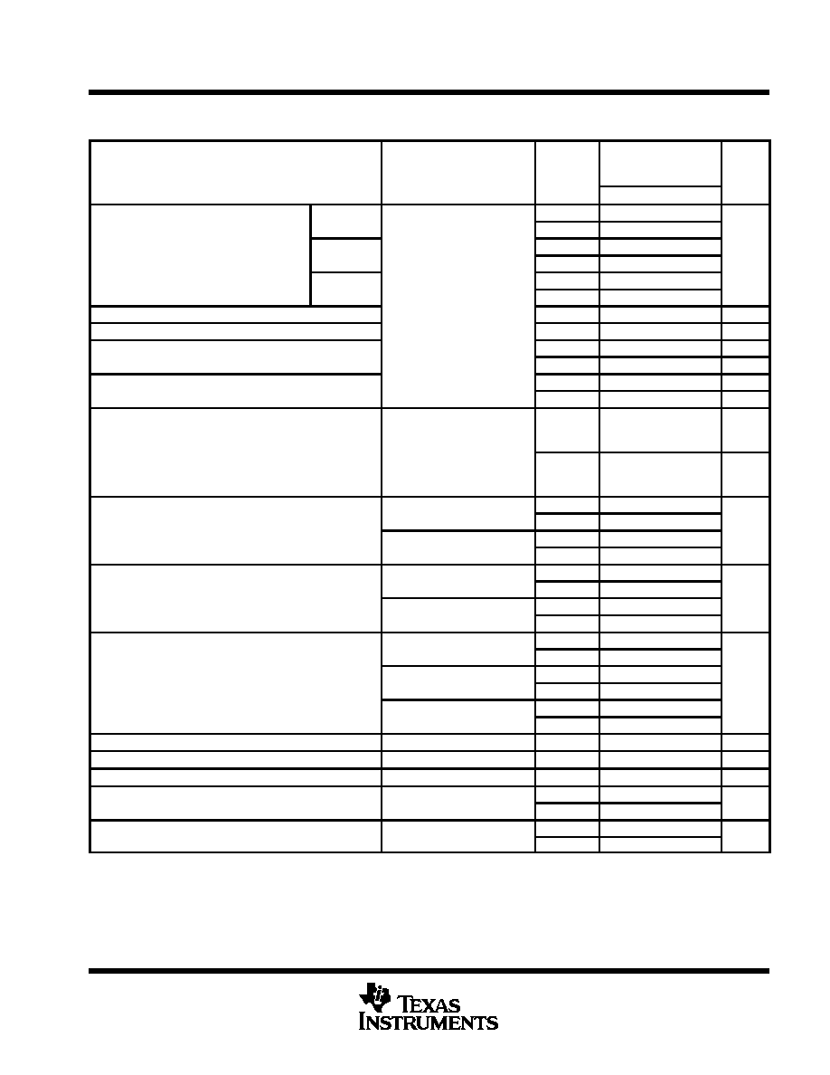
TLE206x, TLE206xA, TLE206xB, TLE206xY
EXCALIBUR JFET-INPUT HIGH-OUTPUT-DRIVE
µ
POWER OPERATIONAL AMPLIFIERS
SLOS193A ≠ FEBRUARY 1997 ≠ REVISED MARCH 1998
35
POST OFFICE BOX 655303
∑
DALLAS, TEXAS 75265
TLE2064C electrical characteristics at specified free-air temperature, V
CC
±
=
±
5 V (unless
otherwise noted)
PARAMETER
TEST CONDITIONS
TA
TLE2064C
TLE2064AC
TLE2064BC
UNIT
MIN
TYP
MAX
TLE2064C
25
∞
C
1.2
7
TLE2064C
Full range
7.9
VIO
Input offset voltage
TLE2064AC
25
∞
C
1.2
6
mV
VIO
Input offset voltage
TLE2064AC
Full range
6.9
mV
TLE2064BC
25
∞
C
0.8
3.5
TLE2064BC
VIC = 0
RS = 50
Full range
4.4
VIO
Temperature coefficient of input offset voltage
VIC = 0,
RS = 50
25
∞
C
6
µ
V/
∞
C
Input offset voltage long-term drift (see Note 4)
Full range
0.04
µ
V/mo
IIO
Input offset current
25
∞
C
1
pA
IIO
Input offset current
Full range
0.8
nA
IIB
Input bias current
25
∞
C
3
pA
IIB
Input bias current
Full range
2
nA
VICR
Common mode input voltage range
25
∞
C
≠ 1.6
to
4
≠ 2
to
6
V
VICR
Common-mode input voltage range
Full range
≠ 1.6
to
4
V
RL = 10 k
25
∞
C
3.5
3.7
VOM
Maximum positive peak output voltage swing
RL = 10 k
Full range
3.3
V
VOM +
Maximum positive peak output voltage swing
RL = 100
25
∞
C
2.5
3.1
V
RL = 100
Full range
2
RL = 10 k
25
∞
C
≠ 3.7
≠ 3.9
VOM
Maximum negative peak output voltage swing
RL = 10 k
Full range
≠ 3.3
V
VOM ≠
Maximum negative peak output voltage swing
RL = 100
25
∞
C
≠ 2.5
≠ 2.7
V
RL = 100
Full range
≠ 2
VO =
±
2 8 V
RL = 10 k
25
∞
C
15
80
VO =
±
2.8 V,
RL = 10 k
Full range
2
A VD
Large signal differential voltage amplification
VO = 0 to 2 V
RL = 100
25
∞
C
0.75
45
V/mV
A VD
Large-signal differential voltage amplification
VO = 0 to 2 V,
RL = 100
Full range
0.5
V/mV
VO = 0 to 2 V
RL = 100
25
∞
C
0.5
3
VO = 0 to ≠ 2 V, RL = 100
Full range
0.15
ri
Input resistance
25
∞
C
1012
ci
Input capacitance
25
∞
C
4
pF
zo
Open-loop output impedance
IO = 0
25
∞
C
560
CMRR
Common mode rejection ratio
VIC = VICRmin
RS = 50
25
∞
C
65
82
dB
CMRR
Common-mode rejection ratio
VIC = VICRmin, RS = 50
Full range
65
dB
kSVR
Supply voltage rejection ratio (
VCC
±
/
VIO)
VCC
±
=
±
5 V to
±
15 V,
25
∞
C
75
93
dB
kSVR
Supply-voltage rejection ratio (
VCC
±
/
VIO)
CC
±
RS = 50
Full range
75
dB
Full range is 0
∞
C to 70
∞
C.
NOTE 4: Typical values are based on the input offset voltage shift observed through 168 hours of operating life test at TA = 150
∞
C extrapolated
to TA = 25
∞
C using the Arrhenius equation and assuming an activation energy of 0.96 eV.
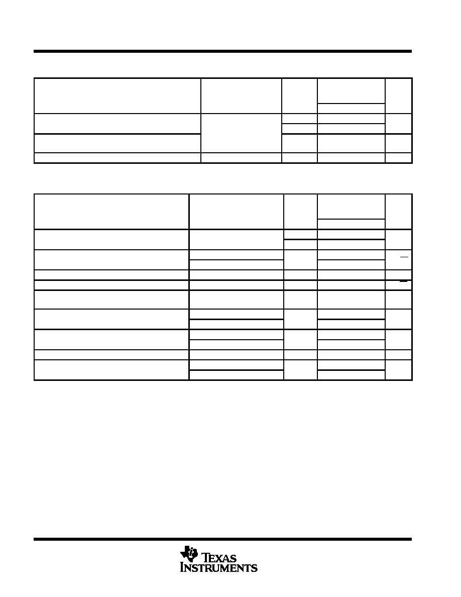
TLE206x, TLE206xA, TLE206xB, TLE206xY
EXCALIBUR JFET-INPUT HIGH-OUTPUT-DRIVE
µ
POWER OPERATIONAL AMPLIFIERS
SLOS193A ≠ FEBRUARY 1997 ≠ REVISED MARCH 1998
36
POST OFFICE BOX 655303
∑
DALLAS, TEXAS 75265
TLE2064C electrical characteristics at specified free-air temperature, V
CC
±
=
±
5 V (unless
otherwise noted) (continued)
PARAMETER
TEST CONDITIONS
TA
TLE2064C
TLE2064AC
TLE2064BC
UNIT
MIN
TYP
MAX
ICC
Supply current (four amplifiers)
25
∞
C
1.12
1.3
mA
ICC
Supply current (four amplifiers)
VO = 0
No load
Full range
1.3
mA
ICC
Supply-current change over operating
VO = 0,
No load
Full range
52
µ
A
ICC
y
g
g
temperature range (four amplifiers)
Full range
52
µ
A
VO1/ VO2 Crosstalk attenuation
AVD = 1000,
f = 1 kHz
25
∞
C
120
dB
Full range is 0
∞
C to 70
∞
C.
TLE2064C operating characteristics at specified free-air temperature, V
CC
±
=
±
5 V
PARAMETER
TEST CONDITIONS
TA
TLE2064C
TLE2064AC
TLE2064BC
UNIT
MIN
TYP
MAX
SR
Slew rate at unity gain (see Figure 1)
RL = 10 k
CL = 100 pF
25
∞
C
2.2
3.4
V/
µ
s
SR
Slew rate at unity gain (see Figure 1)
RL = 10 k
,
CL = 100 pF
Full range
2.1
V/
µ
s
V
Equivalent input noise voltage (see Figure 2)
f = 10 Hz,
RS = 20
25
∞
C
59
100
nV/
H
Vn
Equivalent input noise voltage (see Figure 2)
f = 1 kHz ,
RS = 20
25
∞
C
43
60
nV/
Hz
VN(PP)
Peak-to-peak equivalent input noise voltage
f = 0.1 Hz to 10 Hz
25
∞
C
1.1
µ
V
In
Equivalent input noise current
f = 1 kHz
25
∞
C
1
fA/
Hz
THD
Total harmonic distortion
A VD
= 2,
f = 10 kHz,
25
∞
C
0 025%
THD
Total harmonic distortion
VD
,
VO(PP) = 2 V,
,
RL = 10 k
25
∞
C
0.025%
B1
Unity gain bandwidth (see Figure 3)
RL = 10 k
,
CL = 100 pF
25
∞
C
1.8
MHz
B1
Unity-gain bandwidth (see Figure 3)
RL
= 100
,
CL = 100 pF
25
∞
C
1.3
MHz
t
Settling time
= 0.1%
25
∞
C
5
µ
s
ts
Settling time
= 0.01%
25
∞
C
10
µ
s
BOM
Maximum output-swing bandwidth
A VD = 1,
RL
= 10 k
25
∞
C
140
kHz
Phase margin at unity gain (see Figure 3)
RL
= 10 k
,
CL = 100 pF
25
∞
C
58
∞
m
Phase margin at unity gain (see Figure 3)
RL
= 100
,
CL = 100 pF
25
∞
C
75
∞
Full range is 0
∞
C to 70
∞
C.
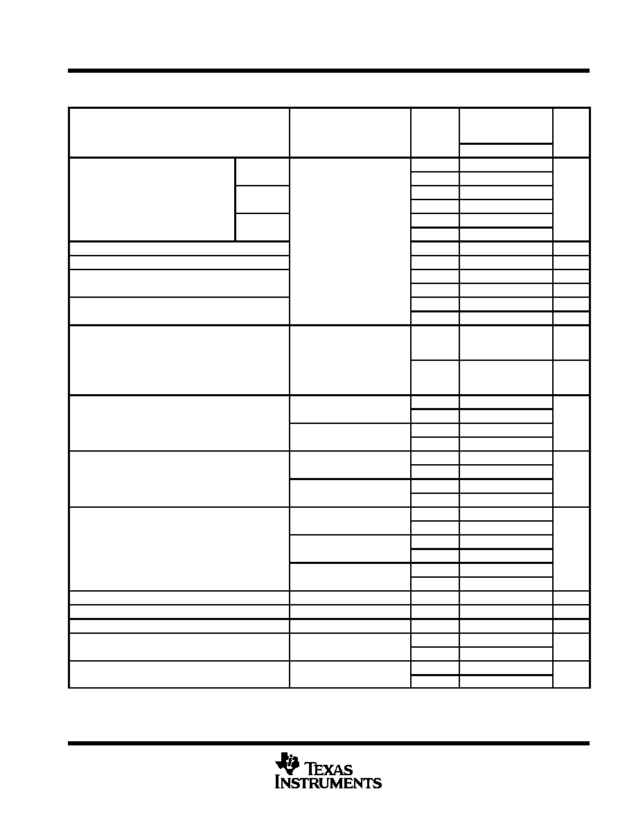
TLE206x, TLE206xA, TLE206xB, TLE206xY
EXCALIBUR JFET-INPUT HIGH-OUTPUT-DRIVE
µ
POWER OPERATIONAL AMPLIFIERS
SLOS193A ≠ FEBRUARY 1997 ≠ REVISED MARCH 1998
37
POST OFFICE BOX 655303
∑
DALLAS, TEXAS 75265
TLE2064C electrical characteristics at specified free-air temperature, V
CC
±
=
±
15 V (unless
otherwise noted)
PARAMETER
TEST CONDITIONS
TA
TLE2064C
TLE2064AC
TLE2064BC
UNIT
MIN
TYP
MAX
TLE2064C
25
∞
C
0.9
6
TLE2064C
Full range
6.9
VIO
Input offset voltage
TLE2064AC
25
∞
C
0.9
4
mV
VIO
Input offset voltage
TLE2064AC
Full range
4.9
mV
TLE2064BC
25
∞
C
0.7
2
TLE2064BC
VIC = 0
RS = 50
Full range
4
VIO
Temperature coefficient of input offset voltage
VIC = 0,
RS = 50
25
∞
C
6
µ
V/
∞
C
Input offset voltage long-term drift (see Note 4)
Full range
0.04
µ
V/mo
IIO
Input offset current
25
∞
C
2
pA
IIO
Input offset current
Full range
1
nA
IIB
Input bias current
25
∞
C
4
pA
IIB
Input bias current
Full range
3
nA
VICR
Common mode input voltage range
25
∞
C
≠ 11
to
13
≠ 12
to
16
V
VICR
Common-mode input voltage range
Full range
≠ 11
to
13
V
RL = 10 k
25
∞
C
13.2
13.7
VOM
Maximum positive peak output voltage swing
RL = 10 k
Full range
13
V
VOM +
Maximum positive peak output voltage swing
RL = 600
25
∞
C
12.5
13.2
V
RL = 600
Full range
12
RL = 10 k
25
∞
C
≠ 13.2
≠ 13.7
VOM
Maximum negative peak output voltage swing
RL = 10 k
Full range
≠ 13
V
VOM ≠
Maximum negative peak output voltage swing
RL = 600
25
∞
C
≠1 2.5
≠ 13
V
RL = 600
Full range
≠ 12
VO =
±
10 V
RL = 10 k
25
∞
C
30
230
VO =
±
10 V,
RL = 10 k
Full range
20
A VD
Large signal differential voltage amplification
VO = 0 to 8 V
RL = 600
25
∞
C
25
100
V/mV
A VD
Large-signal differential voltage amplification
VO = 0 to 8 V,
RL = 600
Full range
10
V/mV
VO = 0 to 8 V
RL = 600
25
∞
C
3
25
VO = 0 to ≠ 8 V,
RL = 600
Full range
1
ri
Input resistance
25
∞
C
1012
ci
Input capacitance
25
∞
C
4
pF
zo
Open-loop output impedance
IO = 0
25
∞
C
560
CMRR
Common mode rejection ratio
VIC = VICRmin
RS = 50
25
∞
C
72
90
dB
CMRR
Common-mode rejection ratio
VIC = VICRmin, RS = 50
Full range
70
dB
kSVR
Supply voltage rejection ratio (
VCC
±
/
VIO)
VCC
±
=
±
5 V to
±
15 V,
25
∞
C
75
93
dB
kSVR
Supply-voltage rejection ratio (
VCC
±
/
VIO)
CC
±
,
RS = 50
Full range
75
dB
Full range is 0
∞
C to 70
∞
C.
NOTE 4: Typical values are based on the input offset voltage shift observed through 168 hours of operating life test at TA = 150
∞
C extrapolated
to TA = 25
∞
C using the Arrhenius equation and assuming an activation energy of 0.96 eV.
TLE206x, TLE206xA, TLE206xB, TLE206xY
EXCALIBUR JFET-INPUT HIGH-OUTPUT-DRIVE
µ
POWER OPERATIONAL AMPLIFIERS
SLOS193A ≠ FEBRUARY 1997 ≠ REVISED MARCH 1998
38
POST OFFICE BOX 655303
∑
DALLAS, TEXAS 75265
TLE2064C electrical characteristics at specified free-air temperature, V
CC
±
=
±
15 V (unless
otherwise noted) (continued)
PARAMETER
TEST CONDITIONS
TA
TLE2064C
TLE2064AC
TLE2064BC
UNIT
MIN
TYP
MAX
ICC
Supply current (four amplifiers)
25
∞
C
1.25
1.4
mA
ICC
Supply current (four amplifiers)
VO = 0
No load
Full range
1.5
mA
ICC
Supply-current change over operating
VO = 0,
No load
Full range
72
µ
A
ICC
y
g
g
temperature range (four amplifiers)
Full range
72
µ
A
VO1/ VO2 Crosstalk attenuation
AVD = 1000, f = 1 kHz
25
∞
C
120
dB
Full range is 0
∞
C to 70
∞
C.
TLE2064C operating characteristics at specified free-air temperature, V
CC
±
=
±
15 V
PARAMETER
TEST CONDITIONS
TA
TLE2064C
TLE2064AC
TLE2064BC
UNIT
MIN
TYP
MAX
SR
Slew rate at unity gain (see Figure 1)
RL = 10 k
CL = 100 pF
25
∞
C
2.6
3.4
V/
µ
s
SR
Slew rate at unity gain (see Figure 1)
RL = 10 k
,
CL = 100 pF
Full range
2.5
V/
µ
s
V
Equivalent input noise voltage (see Figure 2)
f = 10 Hz,
RS = 20
25
∞
C
70
100
nV/
H
Vn
Equivalent input noise voltage (see Figure 2)
f = 1 kHz ,
RS = 20
25
∞
C
40
60
nV/
Hz
VN(PP)
Peak-to-peak equivalent input noise voltage
f = 0.1 Hz to 10 Hz
25
∞
C
1.1
µ
V
In
Equivalent input noise current
f = 1 kHz
25
∞
C
1
fA/
Hz
THD
Total harmonic distortion
A VD
= 2,
f = 10 kHz,
25
∞
C
0 025%
THD
Total harmonic distortion
VD
,
VO(PP) = 2 V,
,
RL = 10 k
25
∞
C
0.025%
B1
Unity gain bandwidth (see Figure 3)
RL = 10 k
,
CL = 100 pF
25
∞
C
2
MHz
B1
Unity-gain bandwidth (see Figure 3)
RL
= 600
,
CL = 100 pF
25
∞
C
1.5
MHz
t
Settling time
= 0.1%
25
∞
C
5
µ
s
ts
Settling time
= 0.01%
25
∞
C
10
µ
s
BOM
Maximum output-swing bandwidth
A VD = 1,
RL
= 10 k
25
∞
C
40
kHz
Phase margin at unity gain (see Figure 3)
RL
= 10 k
,
CL = 100 pF
25
∞
C
50
∞
m
Phase margin at unity gain (see Figure 3)
RL
= 600
,
CL = 100 pF
25
∞
C
70
∞
Full range is 0
∞
C to 70
∞
C.
TLE206x, TLE206xA, TLE206xB, TLE206xY
EXCALIBUR JFET-INPUT HIGH-OUTPUT-DRIVE
µ
POWER OPERATIONAL AMPLIFIERS
SLOS193A ≠ FEBRUARY 1997 ≠ REVISED MARCH 1998
39
POST OFFICE BOX 655303
∑
DALLAS, TEXAS 75265
TLE2064I electrical characteristics at specified free-air temperature, V
CC
±
=
±
5 V (unless otherwise
noted)
PARAMETER
TEST CONDITIONS
TA
TLE2064I
TLE2064AI
TLE2064BI
UNIT
MIN
TYP
MAX
TLE2064I
25
∞
C
1.2
7
TLE2064I
Full range
8.3
VIO
Input offset voltage
TLE2064AI
25
∞
C
1.2
6
mV
VIO
Input offset voltage
TLE2064AI
Full range
7.3
mV
TLE2064BI
25
∞
C
0.8
3.5
TLE2064BI
VIC = 0
RS = 50
Full range
4.8
VIO
Temperature coefficient of input offset voltage
VIC = 0,
RS = 50
25
∞
C
6
µ
V/
∞
C
Input offset voltage long-term drift (see Note 4)
Full range
0.04
µ
V/mo
IIO
Input offset current
25
∞
C
1
pA
IIO
Input offset current
Full range
2
nA
IIB
Input bias current
25
∞
C
3
pA
IIB
Input bias current
Full range
4
nA
VICR
Common mode input voltage range
25
∞
C
≠ 1.6
to
4
≠ 2
to
6
V
VICR
Common-mode input voltage range
Full range
≠ 1.6
to
4
V
RL = 10 k
25
∞
C
3.5
3.7
VOM
Maximum positive peak output voltage swing
RL = 10 k
Full range
3.1
V
VOM +
Maximum positive peak output voltage swing
RL = 100
25
∞
C
2.5
3.1
V
RL = 100
Full range
2
RL = 10 k
25
∞
C
≠ 3.7
≠ 3.9
VOM
Maximum negative peak output voltage swing
RL = 10 k
Full range
≠ 3.1
V
VOM ≠
Maximum negative peak output voltage swing
RL = 100
25
∞
C
≠ 2.5
≠ 2.7
V
RL = 100
Full range
≠ 2
VO =
±
2 8 V
RL = 10 k
25
∞
C
15
80
VO =
±
2.8 V,
RL = 10 k
Full range
2
A VD
Large signal differential voltage amplification
VO = 0 to 2 V
RL = 100
25
∞
C
0.75
45
V/mV
A VD
Large-signal differential voltage amplification
VO = 0 to 2 V,
RL = 100
Full range
0.5
V/mV
VO = 0 to 2 V
RL = 100
25
∞
C
0.5
3
VO = 0 to ≠ 2 V, RL = 100
Full range
0.15
ri
Input resistance
25
∞
C
1012
ci
Input capacitance
25
∞
C
4
pF
zo
Open-loop output impedance
IO = 0
25
∞
C
560
CMRR
Common mode rejection ratio
VIC = VICRmin
RS = 50
25
∞
C
65
82
dB
CMRR
Common-mode rejection ratio
VIC = VICRmin, RS = 50
Full range
65
dB
kSVR
Supply voltage rejection ratio (
VCC
±
/
VIO)
VCC
±
=
±
5 V to
±
15 V,
25
∞
C
75
93
dB
kSVR
Supply-voltage rejection ratio (
VCC
±
/
VIO)
CC
±
RS = 50
Full range
65
dB
Full range is ≠ 40
∞
C to 85
∞
C.
NOTE 4: Typical values are based on the input offset voltage shift observed through 168 hours of operating life test at TA = 150
∞
C extrapolated
to TA = 25
∞
C using the Arrhenius equation and assuming an activation energy of 0.96 eV.
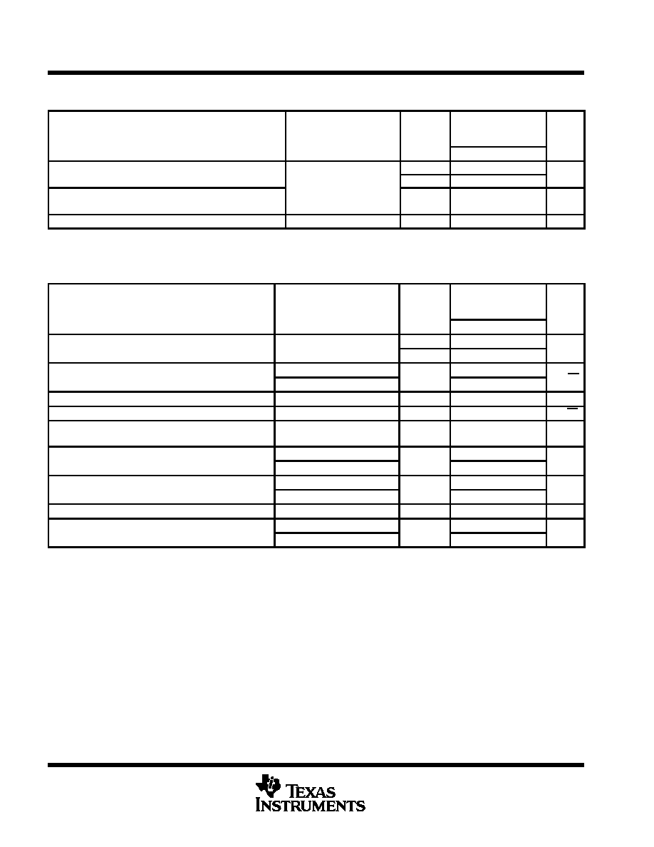
TLE206x, TLE206xA, TLE206xB, TLE206xY
EXCALIBUR JFET-INPUT HIGH-OUTPUT-DRIVE
µ
POWER OPERATIONAL AMPLIFIERS
SLOS193A ≠ FEBRUARY 1997 ≠ REVISED MARCH 1998
40
POST OFFICE BOX 655303
∑
DALLAS, TEXAS 75265
TLE2064I electrical characteristics at specified free-air temperature, V
CC
±
=
±
5 V (unless otherwise
noted) (continued)
PARAMETER
TEST CONDITIONS
TA
TLE2064I
TLE2064AI
TLE2064BI
UNIT
MIN
TYP
MAX
ICC
Supply current (four amplifiers)
25
∞
C
1.12
1.3
mA
ICC
Supply current (four amplifiers)
VO = 0
No load
Full range
1.3
mA
ICC
Supply-current change over operating
VO = 0,
No load
Full range
108
µ
A
ICC
y
g
g
temperature range (four amplifiers)
Full range
108
µ
A
VO1/ VO2 Crosstalk attenuation
AVD = 1000,
f = 1 kHz
25
∞
C
120
dB
Full range is ≠ 40
∞
C to 85
∞
C.
TLE2064I operating characteristics at specified free-air temperature, V
CC
±
=
±
5 V (unless otherwise
noted)
PARAMETER
TEST CONDITIONS
TA
TLE2064I
TLE2064AI
TLE2064BI
UNIT
MIN
TYP
MAX
SR
Slew rate at unity gain (see Figure 1)
RL = 10 k
CL = 100 pF
25
∞
C
2.2
3.4
V/
µ
s
SR
Slew rate at unity gain (see Figure 1)
RL = 10 k
,
CL = 100 pF
Full range
1.7
V/
µ
s
V
Equivalent input noise voltage (see Figure 2)
f = 10 Hz,
RS = 20
25
∞
C
59
100
nV/
H
Vn
Equivalent input noise voltage (see Figure 2)
f = 1 kHz ,
f = 1 kHz ,
25
∞
C
43
60
nV/
Hz
VN(PP)
Peak-to-peak equivalent input noise voltage
f = 0.1 Hz to 10 Hz
25
∞
C
1.1
µ
V
In
Equivalent input noise current
f = 1 kHz
25
∞
C
1
fA/
Hz
THD
Total harmonic distortion
A VD
= 2,
VO(PP) = 2 V,
f = 10 kHz,
RL = 10 k
25
∞
C
0.025%
B1
Unity gain bandwidth (see Figure 3)
RL = 10 k
,
CL = 100 pF
25
∞
C
1.8
MHz
B1
Unity-gain bandwidth (see Figure 3)
RL
= 100
,
CL = 100 pF
25
∞
C
1.3
MHz
t
Settling time
= 0.1%
25
∞
C
5
µ
s
ts
Settling time
= 0.01%
25
∞
C
10
µ
s
BOM
Maximum output-swing bandwidth
A VD = 1,
RL
= 10 k
25
∞
C
140
kHz
Phase margin at unity gain (see Figure 3)
RL
= 10 k
,
CL = 100 pF
25
∞
C
58
∞
m
Phase margin at unity gain (see Figure 3)
RL
= 100
,
CL = 100 pF
25
∞
C
75
∞
Full range is ≠ 40
∞
C to 85
∞
C.
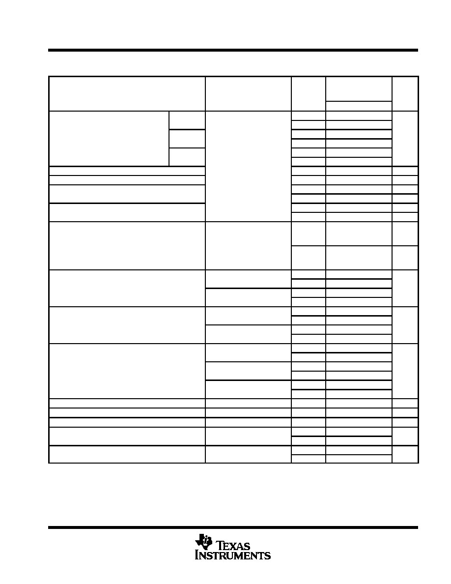
TLE206x, TLE206xA, TLE206xB, TLE206xY
EXCALIBUR JFET-INPUT HIGH-OUTPUT-DRIVE
µ
POWER OPERATIONAL AMPLIFIERS
SLOS193A ≠ FEBRUARY 1997 ≠ REVISED MARCH 1998
41
POST OFFICE BOX 655303
∑
DALLAS, TEXAS 75265
TLE2064I electrical characteristics at specified free-air temperature, V
CC
±
=
±
15 V (unless
otherwise noted)
PARAMETER
TEST CONDITIONS
TA
TLE2064I
TLE2064AI
TLE2064BI
UNIT
MIN
TYP
MAX
TLE2064I
25
∞
C
0.9
6
TLE2064I
Full range
7.3
VIO
Input offset voltage
TLE2064AI
25
∞
C
0.9
4
mV
VIO
Input offset voltage
TLE2064AI
Full range
5.3
mV
TLE2064BI
25
∞
C
0.7
2
TLE2064BI
VIC = 0
RS = 50
Full range
3.3
VIO
Temperature coefficient of input offset voltage
VIC = 0,
RS = 50
25
∞
C
6
µ
V/
∞
C
Input offset voltage long-term drift (see Note 4)
Full range
0.04
µ
V/mo
IIO
Input offset current
25
∞
C
2
pA
IIO
Input offset current
Full range
3
nA
IIB
Input bias current
25
∞
C
4
pA
IIB
Input bias current
Full range
5
nA
VICR
Common mode input voltage range
25
∞
C
≠ 11
to
13
≠ 12
to
16
V
VICR
Common-mode input voltage range
Full range
≠ 11
to
13
V
RL = 10 k
25
∞
C
13.2
13.7
VOM
Maximum positive peak output voltage swing
RL = 10 k
Full range
13
V
VOM +
Maximum positive peak output voltage swing
RL = 600
25
∞
C
12.5
13.2
V
RL = 600
Full range
12
RL = 10 k
25
∞
C
≠ 13.2
≠ 13.7
VOM
Maximum negative peak output voltage swing
RL = 10 k
Full range
≠ 13
V
VOM ≠
Maximum negative peak output voltage swing
RL = 600
25
∞
C
≠12.5
≠ 13
V
RL = 600
Full range
≠ 12
VO =
±
10 V
RL = 10 k
25
∞
C
30
230
VO =
±
10 V,
RL = 10 k
Full range
20
A VD
Large signal differential voltage amplification
VO = 0 to 8 V
RL = 600
25
∞
C
25
100
V/mV
A VD
Large-signal differential voltage amplification
VO = 0 to 8 V,
RL = 600
Full range
10
V/mV
VO = 0 to 8 V
RL = 600
25
∞
C
3
25
VO = 0 to ≠ 8 V,
RL = 600
Full range
1
ri
Input resistance
25
∞
C
1012
ci
Input capacitance
25
∞
C
4
pF
zo
Open-loop output impedance
IO = 0
25
∞
C
560
CMRR
Common mode rejection ratio
VIC = VICRmin
RS = 50
25
∞
C
72
90
dB
CMRR
Common-mode rejection ratio
VIC = VICRmin, RS = 50
Full range
65
dB
kSVR
Supply voltage rejection ratio (
VCC
±
/
VIO)
VCC
±
=
±
5 V to
±
15 V,
25
∞
C
75
93
dB
kSVR
Supply-voltage rejection ratio (
VCC
±
/
VIO)
CC
±
RS = 50
Full range
65
dB
Full range is ≠ 40
∞
C to 85
∞
C.
NOTE 4: Typical values are based on the input offset voltage shift observed through 168 hours of operating life test at TA = 150
∞
C extrapolated
to TA = 25
∞
C using the Arrhenius equation and assuming an activation energy of 0.96 eV.
TLE206x, TLE206xA, TLE206xB, TLE206xY
EXCALIBUR JFET-INPUT HIGH-OUTPUT-DRIVE
µ
POWER OPERATIONAL AMPLIFIERS
SLOS193A ≠ FEBRUARY 1997 ≠ REVISED MARCH 1998
42
POST OFFICE BOX 655303
∑
DALLAS, TEXAS 75265
TLE2064I electrical characteristics at specified free-air temperature, V
CC
±
=
±
15 V (unless
otherwise noted) (continued)
PARAMETER
TEST CONDITIONS
TA
TLE2064I
TLE2064AI
TLE2064BI
UNIT
MIN
TYP
MAX
ICC
Supply current (four amplifiers)
25
∞
C
1.25
1.4
mA
ICC
Supply current (four amplifiers)
VO = 0
No load
Full range
1.5
mA
ICC
Supply-current change over operating
VO = 0,
No load
Full range
148
µ
A
ICC
y
g
g
temperature range (four amplifiers)
Full range
148
µ
A
VO1/ VO2 Crosstalk attenuation
AVD = 1000,
f = 1 kHz
25
∞
C
120
dB
Full range is ≠ 40
∞
C to 85
∞
C.
TLE2064I operating characteristics at specified free-air temperature, V
CC
±
=
±
15 V
PARAMETER
TEST CONDITIONS
TA
TLE2064I
TLE2064AI
TLE2064BI
UNIT
MIN
TYP
MAX
SR
Slew rate at unity gain (see Figure 1)
RL = 10 k
CL = 100 pF
25
∞
C
2.6
3.4
V/
µ
s
SR
Slew rate at unity gain (see Figure 1)
RL = 10 k
,
CL = 100 pF
Full range
2.1
V/
µ
s
V
Equivalent input noise voltage (see Figure 2)
f = 10 Hz,
RS = 20
,
25
∞
C
70
100
nV/
H
Vn
Equivalent input noise voltage (see Figure 2)
f = 1 kHz ,
RS = 20
25
∞
C
40
60
nV/
Hz
VN(PP)
Peak-to-peak equivalent input noise voltage
f = 0.1 Hz to 10 Hz
25
∞
C
1.1
µ
V
In
Equivalent input noise current
f = 1 kHz
25
∞
C
1.1
fA/
Hz
THD
Total harmonic distortion
A VD
= 2,
f = 10 kHz,
25
∞
C
0 025%
THD
Total harmonic distortion
VD
,
RL = 10 k
,
VO(PP) = 2 V,
25
∞
C
0.025%
B1
Unity gain bandwidth (see Figure 3)
RL = 10 k
,
CL = 100 pF
25
∞
C
2
MHz
B1
Unity-gain bandwidth (see Figure 3)
RL
= 600
,
CL = 100 pF
25
∞
C
1.5
MHz
t
Settling time
= 0.1%
25
∞
C
5
µ
s
ts
Settling time
= 0.01%
25
∞
C
10
µ
s
BOM
Maximum output-swing bandwidth
A VD = 1,
RL
= 10 k
25
∞
C
40
kHz
Phase margin at unity gain (see Figure 3)
RL
= 10 k
,
CL = 100 pF
25
∞
C
60
∞
m
Phase margin at unity gain (see Figure 3)
RL
= 600
,
CL = 100 pF
25
∞
C
70
∞
Full range is ≠ 40
∞
C to 85
∞
C.
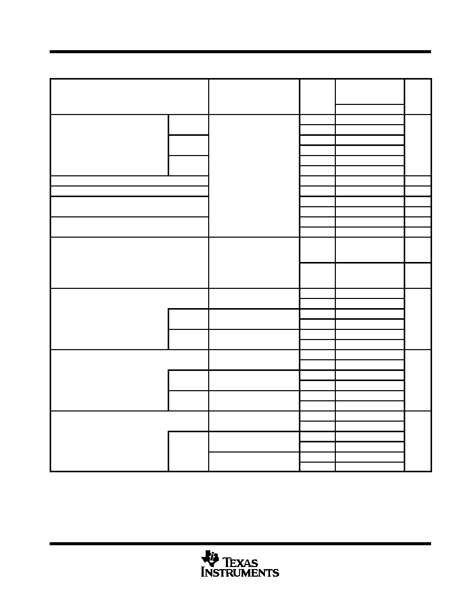
TLE206x, TLE206xA, TLE206xB, TLE206xY
EXCALIBUR JFET-INPUT HIGH-OUTPUT-DRIVE
µ
POWER OPERATIONAL AMPLIFIERS
SLOS193A ≠ FEBRUARY 1997 ≠ REVISED MARCH 1998
43
POST OFFICE BOX 655303
∑
DALLAS, TEXAS 75265
TLE2064M electrical characteristics at specified free-air temperature, V
CC
±
=
±
5 V (unless
otherwise noted)
PARAMETER
TEST CONDITIONS
TA
TLE2064M
TLE2064AM
TLE2064BM
UNIT
MIN
TYP
MAX
TLE2064M
25
∞
C
1.2
7
TLE2064M
Full range
9
VIO
Input offset voltage
TLE2064AM
25
∞
C
1.2
6
mV
VIO
Input offset voltage
TLE2064AM
Full range
8
mV
TLE2064BM
25
∞
C
0.8
3.5
TLE2064BM
VIC = 0
RS = 50
Full range
5.5
VIO
Temperature coefficient of input offset voltage
VIC = 0,
RS = 50
25
∞
C
6
µ
V/
∞
C
Input offset voltage long-term drift (see Note 4)
Full range
0.04
µ
V/mo
IIO
Input offset current
25
∞
C
1
pA
IIO
Input offset current
Full range
15
nA
IIB
Input bias current
25
∞
C
3
pA
IIB
Input bias current
Full range
30
nA
VICR
Common mode input voltage range
25
∞
C
≠ 1.6
to
4
≠ 2
to
6
V
VICR
Common-mode input voltage range
Full range
≠ 1.6
to
4
V
RL = 10 k
25
∞
C
3.5
3.7
RL = 10 k
Full range
3
VOM
Maximum positive peak output
FK and J
RL = 600
25
∞
C
2.5
3.6
V
VOM +
voltage swing
packages
RL = 600
Full range
2
V
D and N
RL = 100
25
∞
C
2.5
3.1
packages
RL = 100
Full range
2
RL = 10 k
25
∞
C
≠ 3.5
≠ 3.9
RL = 10 k
Full range
≠ 3
VOM
Maximum negative peak output
FK and J
RL = 600
25
∞
C
≠ 2.5
≠3.5
V
VOM ≠
g
voltage swing
packages
RL = 600
Full range
≠ 2
V
D and N
RL = 100
25
∞
C
≠ 2.5
≠ 2.7
packages
RL = 100
Full range
≠ 2
VO =
±
2 8 V
RL = 10 k
25
∞
C
15
80
VO =
±
2.8 V,
RL = 10 k
Full range
2
A VD
Large-signal differential voltage
VO = 0 to 2 5 V
RL = 600
25
∞
C
1
65
V/mV
A VD
g
g
g
amplification
FK and J
VO = 0 to 2.5 V,
RL = 600
Full range
0.5
V/mV
packages
VO = 0 to 2 5 V
RL = 600
25
∞
C
1
16
VO = 0 to ≠ 2.5 V, RL = 600
Full range
0.5
Full range is ≠ 55
∞
C to 125
∞
C.
NOTE 4: Typical values are based on the input offset voltage shift observed through 168 hours of operating life test at TA = 150
∞
C extrapolated
to TA = 25
∞
C using the Arrhenius equation and assuming an activation energy of 0.96 eV.
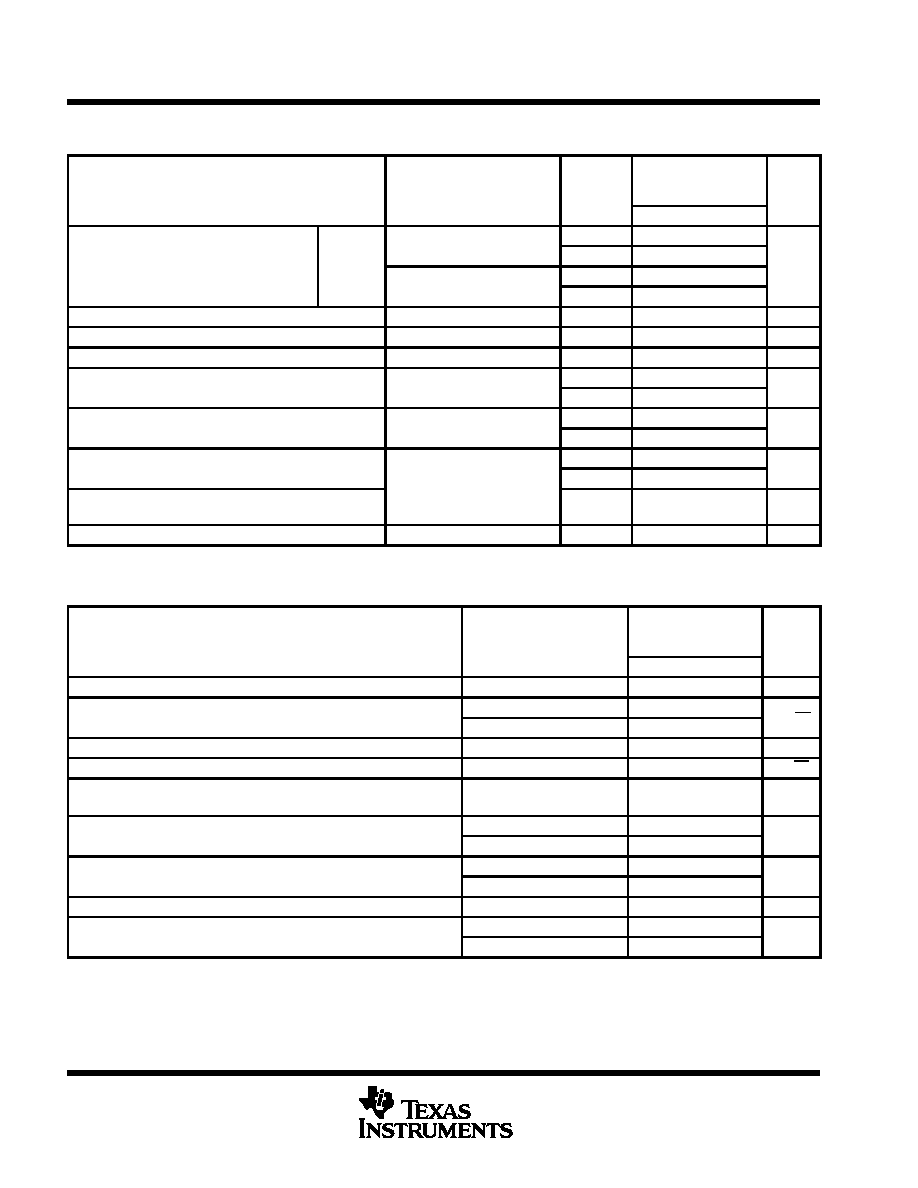
TLE206x, TLE206xA, TLE206xB, TLE206xY
EXCALIBUR JFET-INPUT HIGH-OUTPUT-DRIVE
µ
POWER OPERATIONAL AMPLIFIERS
SLOS193A ≠ FEBRUARY 1997 ≠ REVISED MARCH 1998
44
POST OFFICE BOX 655303
∑
DALLAS, TEXAS 75265
TLE2064M electrical characteristics at specified free-air temperature, V
CC
±
=
±
5 V (unless
otherwise noted) continued)
PARAMETER
TEST CONDITIONS
TA
TLE2064M
TLE2064AM
TLE2064BM
UNIT
MIN
TYP
MAX
VO = 0 to 2 V
RL = 100
25
∞
C
0.75
45
A VD
Large-signal differential voltage
D and N
VO = 0 to 2 V,
RL = 100
Full range
0.25
V/mV
A VD
g
g
g
amplification
packages
VO = 0 to 2 V
RL = 100
25
∞
C
0.4
3
V/mV
VO = 0 to ≠ 2 V, RL = 100
Full range
0.15
ri
Input resistance
25
∞
C
1012
ci
Input capacitance
25
∞
C
4
pF
zo
Open-loop output impedance
IO = 0
25
∞
C
560
CMRR
Common mode rejection ratio
VIC = VICRmin
RS = 50
25
∞
C
65
82
dB
CMRR
Common-mode rejection ratio
VIC = VICRmin, RS = 50
Full range
60
dB
kSVR
Supply voltage rejection ratio (
VCC
±
/
VIO)
VCC
±
=
±
5 V to
±
15 V,
25
∞
C
75
93
dB
kSVR
Supply-voltage rejection ratio (
VCC
±
/
VIO)
CC
±
,
RS = 50
Full range
65
dB
ICC
Supply current (four amplifiers)
25
∞
C
1.12
1.3
mA
ICC
Supply current (four amplifiers)
VO = 0
No load
Full range
1.3
mA
ICC
Supply-current change over operating
temperature range (four amplifiers)
VO = 0,
No load
Full range
144
µ
A
VO1/ VO2 Crosstalk attenuation
AVD = 1000,
f = 1 kHz
25
∞
C
120
dB
Full range is ≠ 55
∞
C to 125
∞
C.
TLE2064M operating characteristics, V
CC
±
=
±
5 V, T
A
= 25
∞
C
PARAMETER
TEST CONDITIONS
TLE2064M
TLE2064AM
TLE2064BM
UNIT
MIN
TYP
MAX
SR
Slew rate at unity gain (see Figure 1)
RL = 10 k
,
CL = 100 pF
3.4
V/
µ
s
V
Equivalent input noise voltage (see Figure 2)
f = 10 Hz,
RS = 20
59
nV/
H
Vn
Equivalent input noise voltage (see Figure 2)
f = 1 kHz ,
RS = 20
43
nV/
Hz
VN(PP)
Peak-to-peak equivalent input noise voltage
f = 0.1 Hz to 10 Hz
1.1
µ
V
In
Equivalent input noise current
f = 1 kHz
1
fA/
Hz
THD
Total harmonic distortion
A VD
= 2,
f = 10 kHz,
0 025%
THD
Total harmonic distortion
VD
,
VO(PP) = 2 V,
,
RL = 10 k
0.025%
B1
Unity gain bandwidth (see Figure 3)
RL = 10 k
,
CL = 100 pF
1.8
MHz
B1
Unity-gain bandwidth (see Figure 3)
RL
= 600
,
CL = 100 pF
1.3
MHz
t
Settling time
= 0.1%
5
µ
s
ts
Settling time
= 0.01%
10
µ
s
BOM
Maximum output-swing bandwidth
A VD = 1,
RL
= 10 k
140
kHz
Phase margin at unity gain (see Figure 3)
RL
= 10 k
,
CL = 100 pF
58
∞
m
Phase margin at unity gain (see Figure 3)
RL
= 600
,
CL = 100 pF
75
∞
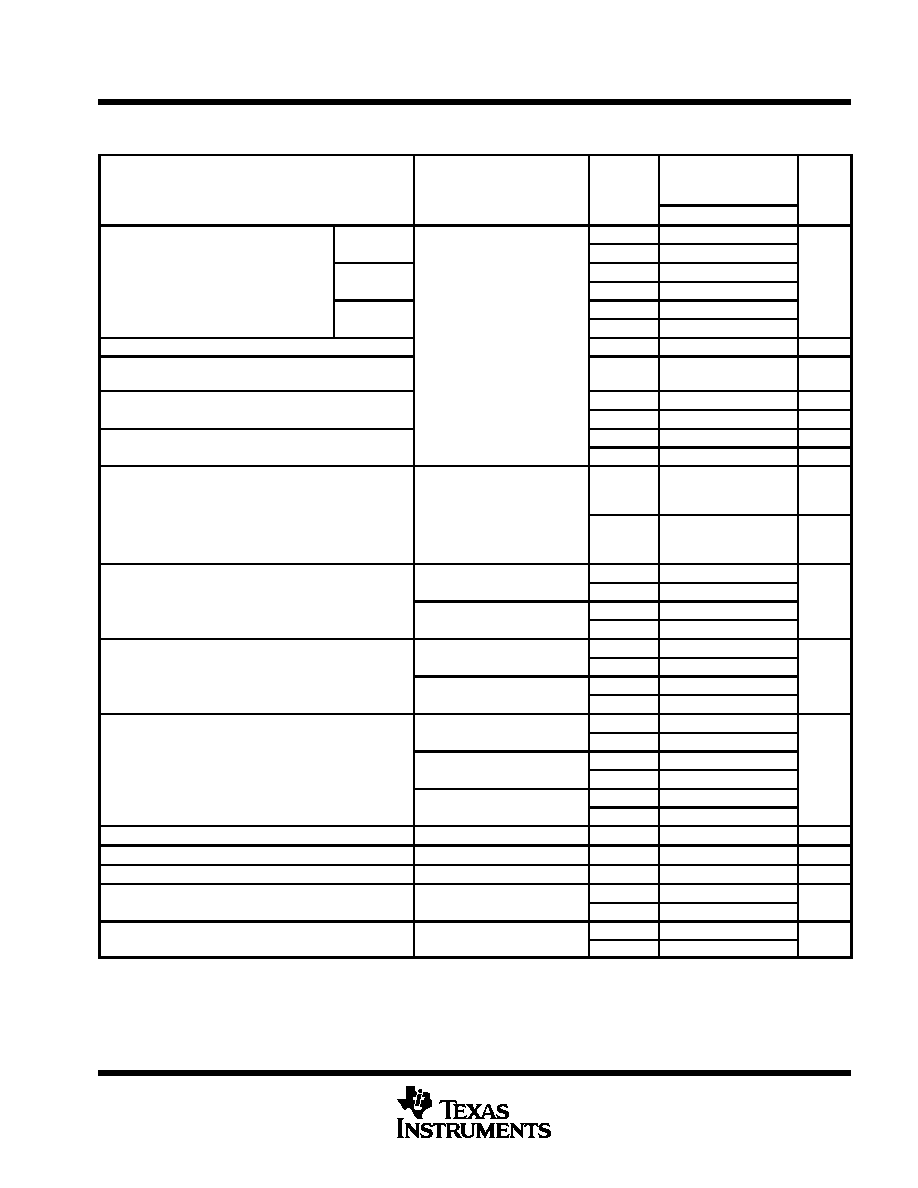
TLE206x, TLE206xA, TLE206xB, TLE206xY
EXCALIBUR JFET-INPUT HIGH-OUTPUT-DRIVE
µ
POWER OPERATIONAL AMPLIFIERS
SLOS193A ≠ FEBRUARY 1997 ≠ REVISED MARCH 1998
45
POST OFFICE BOX 655303
∑
DALLAS, TEXAS 75265
TLE2064M electrical characteristics at specified free-air temperature, V
CC
±
=
±
15 V (unless
otherwise noted)
PARAMETER
TEST CONDITIONS
TA
TLE2064M
TLE2064AM
TLE2064BM
UNIT
MIN
TYP
MAX
TLE2064M
25
∞
C
0.9
6
TLE2064M
Full range
8
VIO
Input offset voltage
TLE2064AM
25
∞
C
0.9
4
mV
VIO
Input offset voltage
TLE2064AM
Full range
6
mV
TLE2064BM
25
∞
C
0.7
2
TLE2064BM
Full range
4
VIO
Temperature coefficient of input offset voltage
VIC = 0,
RS = 50
25
∞
C
6
µ
V/
∞
C
Input offset voltage long-term drift
(see Note 4)
Full range
0.04
µ
V/mo
IIO
Input offset current
25
∞
C
2
pA
IIO
Input offset current
Full range
20
nA
IIB
Input bias current
25
∞
C
4
pA
IIB
Input bias current
Full range
40
nA
VICR
Common mode input voltage range
25
∞
C
≠ 11
to
13
≠ 12
to
16
V
VICR
Common-mode input voltage range
Full range
≠ 11
to
13
V
RL = 10 k
25
∞
C
13
13.7
VOM
Maximum positive peak output voltage swing
RL = 10 k
Full range
12.5
V
VOM +
Maximum positive peak output voltage swing
RL = 600
25
∞
C
12.5
13.2
V
RL = 600
Full range
12
RL = 10 k
25
∞
C
≠ 13
≠ 13.7
VOM
Maximum negative peak output voltage swing
RL = 10 k
Full range
≠ 12.5
V
VOM ≠
Maximum negative peak output voltage swing
RL = 600
25
∞
C
≠13
≠ 13
V
RL = 600
Full range
≠ 12.5
VO =
±
10 V
RL = 10 k
25
∞
C
30
230
VO =
±
10 V,
RL = 10 k
Full range
20
A VD
Large signal differential voltage amplification
VO = 0 to 8 V
RL = 600
25
∞
C
25
100
V/mV
A VD
Large-signal differential voltage amplification
VO = 0 to 8 V,
RL = 600
Full range
7
V/mV
VO = 0 to 8 V
RL = 600
25
∞
C
3
25
VO = 0 to ≠ 8 V,
RL = 600
Full range
1
ri
Input resistance
25
∞
C
1012
ci
Input capacitance
25
∞
C
4
pF
zo
Open-loop output impedance
IO = 0
25
∞
C
560
CMRR
Common mode rejection ratio
VIC = VICRmin
RS = 50
25
∞
C
72
90
dB
CMRR
Common-mode rejection ratio
VIC = VICRmin, RS = 50
Full range
65
dB
kSVR
Supply voltage rejection ratio (
VCC
±
/
VIO)
VCC
±
=
±
5 V to
±
15 V,
25
∞
C
75
93
dB
kSVR
Supply-voltage rejection ratio (
VCC
±
/
VIO)
CC
±
RS = 50
Full range
65
dB
Full range is ≠ 55
∞
C to 125
∞
C.
NOTE 4: Typical values are based on the input offset voltage shift observed through 168 hours of operating life test at TA = 150
∞
C extrapolated
to TA = 25
∞
C using the Arrhenius equation and assuming an activation energy of 0.96 eV.
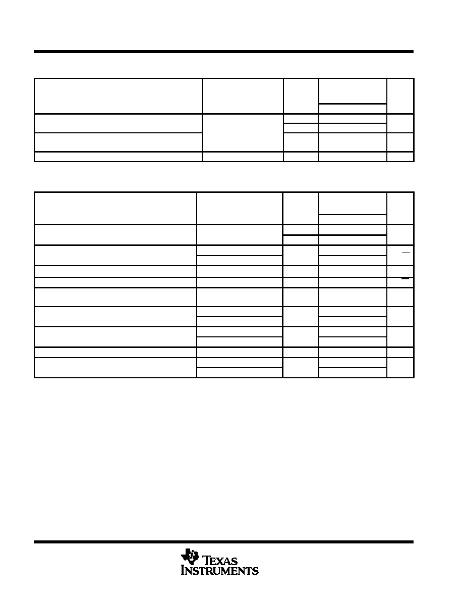
TLE206x, TLE206xA, TLE206xB, TLE206xY
EXCALIBUR JFET-INPUT HIGH-OUTPUT-DRIVE
µ
POWER OPERATIONAL AMPLIFIERS
SLOS193A ≠ FEBRUARY 1997 ≠ REVISED MARCH 1998
46
POST OFFICE BOX 655303
∑
DALLAS, TEXAS 75265
TLE2064M electrical characteristics at specified free-air temperature, V
CC
±
=
±
15 V (unless
otherwise noted) (continued)
PARAMETER
TEST CONDITIONS
TA
TLE2064M
TLE2064AM
TLE2064BM
UNIT
MIN
TYP
MAX
ICC
Supply current (four amplifiers)
25
∞
C
1.25
1.4
mA
ICC
Supply current (four amplifiers)
VO = 0
No load
Full range
1.5
mA
ICC
Supply-current change over operating
VO = 0,
No load
Full range
194
µ
A
ICC
y
g
g
temperature range (four amplifiers)
Full range
194
µ
A
VO1/ VO2 Crosstalk attenuation
AVD = 1000,
f = 1 kHz
25
∞
C
120
dB
Full range is ≠ 55
∞
C to 125
∞
C.
TLE2064M operating characteristics at specified free-air temperature, V
CC
±
=
±
15 V
PARAMETER
TEST CONDITIONS
TA
TLE2064M
TLE2064AM
TLE2064BM
UNIT
MIN
TYP
MAX
SR
Slew rate at unity gain (see Figure 1)
RL = 10 k
CL = 100 pF
25
∞
C
2.6
3.4
V/
µ
s
SR
Slew rate at unity gain (see Figure 1)
RL = 10 k
,
CL = 100 pF
Full range
1.8
V/
µ
s
V
Equivalent input noise voltage (see Figure 2)
f = 10 Hz,
RS = 20
25
∞
C
70
nV/
H
Vn
Equivalent input noise voltage (see Figure 2)
f = 1 kHz ,
RS = 20
25
∞
C
40
nV/
Hz
VN(PP)
Peak to peak equivalent input noise voltage
f = 0 1 Hz to 10 Hz
25
∞
C
1 1
µ
V
VN(PP)
Peak-to-peak equivalent input noise voltage
f = 0.1 Hz to 10 Hz
25
∞
C
1.1
µ
V
In
Equivalent input noise current
f = 1 kHz
25
∞
C
1.1
fA/
Hz
THD
Total harmonic distortion
A VD
= 2,
f = 10 kHz,
25
∞
C
0 025%
THD
Total harmonic distortion
VD
,
VO(PP) = 2 V,
,
RL = 10 k
25
∞
C
0.025%
B1
Unity gain bandwidth (see Figure 3)
RL = 10 k
,
CL = 100 pF
25
∞
C
2
MHz
B1
Unity-gain bandwidth (see Figure 3)
RL
= 600
,
CL = 100 pF
25
∞
C
1.5
MHz
t
Settling time
= 0.1%
25
∞
C
5
µ
s
ts
Settling time
= 0.01%
25
∞
C
10
µ
s
BOM
Maximum output-swing bandwidth
A VD = 1,
RL
= 10 k
25
∞
C
40
kHz
Phase margin at unity gain (see Figure 3)
RL
= 10 k
,
CL = 100 pF
25
∞
C
60
∞
m
Phase margin at unity gain (see Figure 3)
RL
= 600
,
CL = 100 pF
25
∞
C
70
∞
Full range is ≠ 55
∞
C to 125
∞
C.
TLE206x, TLE206xA, TLE206xB, TLE206xY
EXCALIBUR JFET-INPUT HIGH-OUTPUT-DRIVE
µ
POWER OPERATIONAL AMPLIFIERS
SLOS193A ≠ FEBRUARY 1997 ≠ REVISED MARCH 1998
47
POST OFFICE BOX 655303
∑
DALLAS, TEXAS 75265
TLE2064Y electrical characteristics at V
CC
±
=
±
15 V, T
A
= 25
∞
C (unless otherwise noted)
PARAMETER
TEST CONDITIONS
TLE2064Y
UNIT
PARAMETER
TEST CONDITIONS
MIN
TYP
MAX
UNIT
VIO
Input offset voltage
0.9
6
mV
VIO
Input offset voltage long-term drift (see Note 4)
VIC = 0
RS = 50
0.04
µ
V/mo
IIO
Input offset current
VIC = 0,
RS = 50
2
pA
IIB
Input bias current
4
pA
VICR
Common-mode input voltage range
≠ 11
to
13
≠ 12
to
16
V
VOM
Maximum positive peak output voltage swing
RL = 10 k
13.2
13.7
V
VOM +
Maximum positive peak output voltage swing
RL = 600
12.5
13.2
V
VOM
Maximum negative peak output voltage swing
RL = 10 k
≠13.2
≠ 13.7
V
VOM ≠
Maximum negative peak output voltage swing
RL = 600
12.5
13
V
VO =
±
10 V,
RL = 10 k
30
230
A VD
Large-signal differential voltage amplification
VO = 0 to 8 V,
RL = 600
25
100
V/mV
VO = 0 to ≠ 8 V,
RL = 600
3
25
ri
Input resistance
1012
ci
Input capacitance
4
pF
zo
Open-loop output impedance
IO = 0
560
CMRR
Common-mode rejection ratio
RS = 50
,
VIC = VICRmin,
72
90
dB
kSVR
Supply-voltage rejection ratio (
VCC
±
/
VIO)
VCC
±
=
±
5 V to
±
15 V,
RS = 50
75
93
dB
ICC
Supply current
VO = 0,
No load
1.25
1.4
mA
VO1/ VO2 Crosstalk attenuation
AVD = 1000,
f = 1 kHz
120
dB
NOTE 4: Typical values are based on the input offset voltage shift observed through 168 hours of operating life test at TA = 150
∞
C extrapolated
to TA = 25
∞
C using the Arrhenius equation and assuming an activation energy of 0.96 eV.
TLE2064Y operating characteristics at V
CC
±
=
±
15 V, T
A
= 25
∞
C
PARAMETER
TEST CONDITIONS
TLE2064Y
UNIT
PARAMETER
TEST CONDITIONS
MIN
TYP
MAX
UNIT
SR
Slew rate at unity gain (see Figure 1)
RL = 10 k
,
CL = 100 pF
2.6
3.4
V/
µ
s
V
Equivalent input noise voltage (see Figure 2)
f = 10 Hz,
RS = 20
70
nV/
H
Vn
Equivalent input noise voltage (see Figure 2)
f = 1 kHz ,
RS = 20
40
nV/
Hz
VN(PP)
Peak-to-peak equivalent input noise voltage
f = 0.1 Hz to 10 Hz
1.1
µ
V
In
Equivalent input noise current
f = 1 kHz
1.1
fA/
Hz
THD
Total harmonic distortion
A VD
= 2,
f = 10 kHz,
0 025%
THD
Total harmonic distortion
VD
,
VO(PP) = 2 V,
,
RL = 10 k
0.025%
B1
Unity gain bandwidth (see Figure 3)
RL = 10 k
,
CL = 100 pF
2
MHz
B1
Unity-gain bandwidth (see Figure 3)
RL
= 600
,
CL = 100 pF
1.5
MHz
t
Settling time
= 0.1%
5
µ
s
ts
Settling time
= 0.01%
10
µ
s
BOM
Maximum output-swing bandwidth
A VD = 1,
RL
= 10 k
40
kHz
Phase margin at unity gain (see Figure 3)
RL
= 10 k
,
CL = 100 pF
60
∞
m
Phase margin at unity gain (see Figure 3)
RL
= 600
,
CL = 100 pF
70
∞
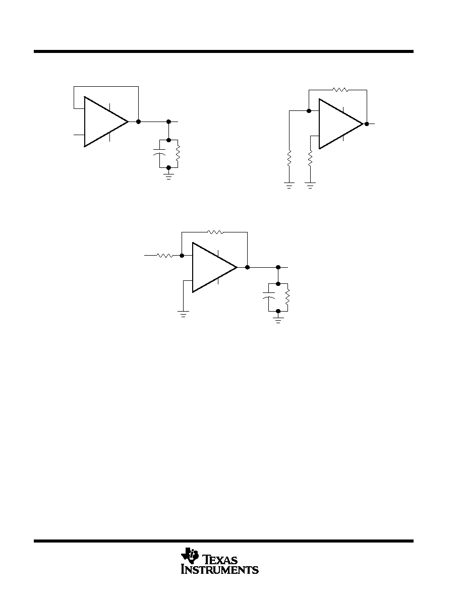
TLE206x, TLE206xA, TLE206xB, TLE206xY
EXCALIBUR JFET-INPUT HIGH-OUTPUT-DRIVE
µ
POWER OPERATIONAL AMPLIFIERS
SLOS193A ≠ FEBRUARY 1997 ≠ REVISED MARCH 1998
48
POST OFFICE BOX 655303
∑
DALLAS, TEXAS 75265
PARAMETER MEASUREMENT INFORMATION
Figure 1. Slew-Rate Test Circuit
RL
(see Note A)
CL
VO
VCC ≠
VI
+
≠
VCC +
NOTE A: CL includes fixture capacitance.
Figure 2. Noise-Voltage Test Circuit
VO
RS
RS
2 k
VCC ≠
VCC +
+
≠
VO
RL
CL
(see Note A)
10 k
100
VI
VCC ≠
VCC +
+
≠
NOTE A: CL includes fixture capacitance.
Figure 3. Unity-Gain Bandwidth and Phase-Margin Test Circuit
typical values
Typical values presented in this data sheet represent the median (50% point) of device parametric performance.
input bias and offset current
At the picoampere bias current level typical of the TLE206x, TLE2064xA, and TLE206xB, accurate
measurement of the bias current becomes difficult. Not only does this measurement require a picoammeter,
but test socket leakages can easily exceed the actual device bias currents. To accurately measure these small
currents, Texas Instruments uses a two-step process. The socket leakage is measured using picoammeters
with bias voltages applied but with no device in the socket. The device is then inserted into the socket, and a
second test that measures both the socket leakage and the device input bias current is performed. The two
measurements are then subtracted algebraically to determine the bias current of the device.
TLE206x, TLE206xA, TLE206xB, TLE206xY
EXCALIBUR JFET-INPUT HIGH-OUTPUT-DRIVE
µ
POWER OPERATIONAL AMPLIFIERS
SLOS193A ≠ FEBRUARY 1997 ≠ REVISED MARCH 1998
49
POST OFFICE BOX 655303
∑
DALLAS, TEXAS 75265
TYPICAL CHARACTERISTICS
Table of Graphs
FIGURE
VIO
Input offset voltage
Distribution
4, 5, 6
IIB
Input bias current
vs Common-mode input voltage
vs Free-air temperature
7
8
IIO
Input offset current
vs Free-air temperature
8
VICR
Common-mode input voltage
vs Free-air temperature
9
VOM
Maximum peak output voltage
vs Output current
vs Supply voltage
10, 11
12, 13, 14
VO(PP)
Maximum peak-to-peak output voltage
vs Frequency
vs Load resistance
15, 16
17
AVD
Large-signal differential voltage amplification
vs Frequency
vs Free-air temperature
18
19
IOS
Short-circuit output current
vs Elasped time
vs Free-air temperature
20
21
zo
Output impedance
vs Frequency
22, 23
CMRR
Common-mode rejection ratio
vs Frequency
24
ICC
Supply current
vs Supply voltage
vs Free-air temperature
25, 26, 27
28, 29, 30
Voltage-follower small-signal pulse response
vs Time
31, 32
Voltage-follower large-signal pulse response
vs Time
33, 34
Noise voltage (referred to input)
0.1 to 10 Hz
35
Vn
Equivalent input noise voltage
vs Frequency
36
THD
Total harmonic distortion
vs Frequency
37, 38
B1
Unity-gain bandwidth
vs Supply voltage
vs Free-air temperature
39
40
m
Phase margin
vs Supply voltage
vs Load capacitance
vs Free-air temperature
41
42
43
Phase shift
vs Frequency
18
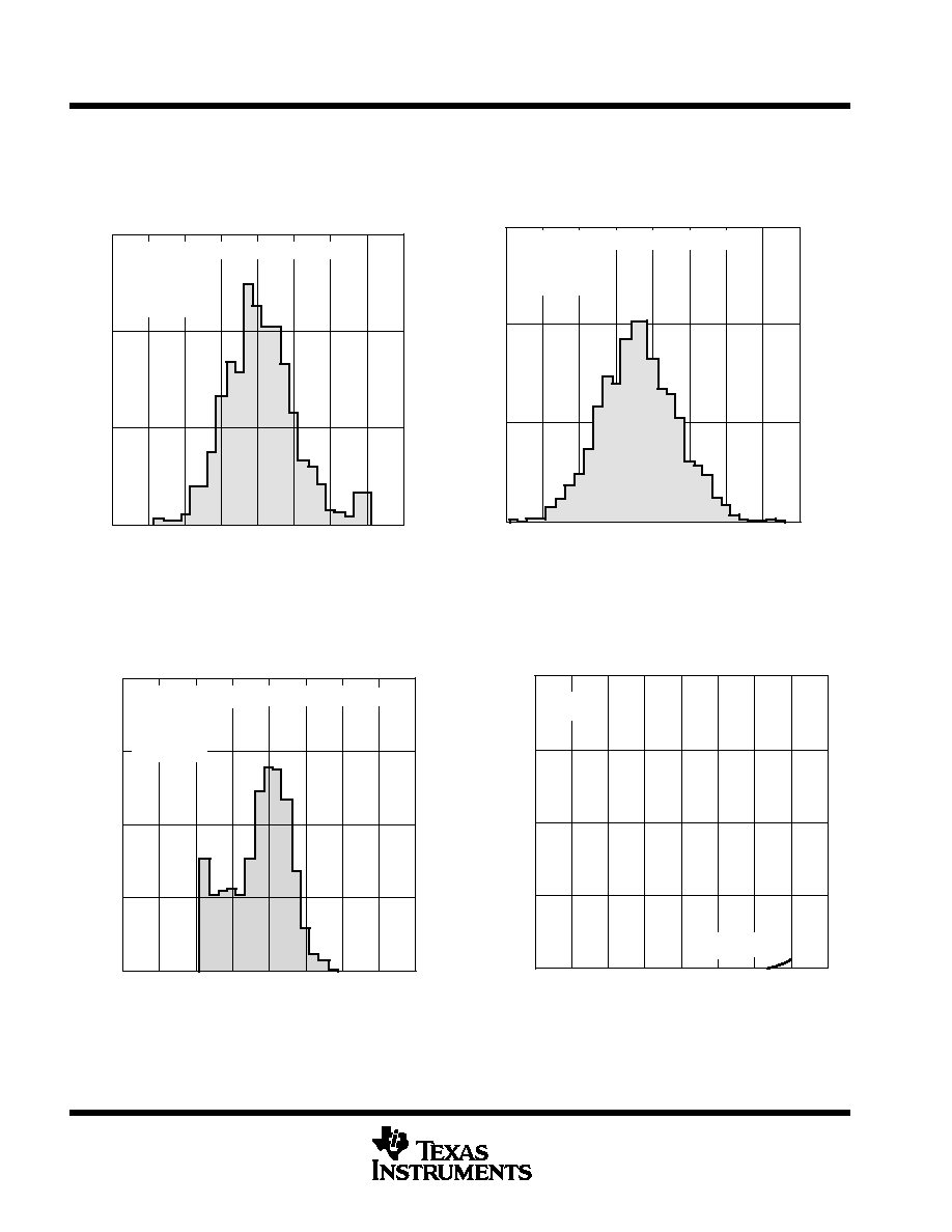
TLE206x, TLE206xA, TLE206xB, TLE206xY
EXCALIBUR JFET-INPUT HIGH-OUTPUT-DRIVE
µ
POWER OPERATIONAL AMPLIFIERS
SLOS193A ≠ FEBRUARY 1997 ≠ REVISED MARCH 1998
50
POST OFFICE BOX 655303
∑
DALLAS, TEXAS 75265
TYPICAL CHARACTERISTICS
Figure 4
TLE2061
DISTRIBUTION OF
INPUT OFFSET VOLTAGE
4
3
2
1
0
≠ 1
≠ 2
≠ 3
≠ 4
VIO ≠ Input Offset Voltage ≠ mV
Percentage
of
Amplifiers
≠
%
0
5
10
15
P Package
TA = 25
∞
C
VCC
±
=
±
15 V
736 Amplifiers Tested From 3 Wafer Lots
Figure 5
VIO ≠ Input Offset Voltage ≠ mV
10
5
0
≠ 2
≠1
0
1
Percentage of
Amplifiers ≠ %
TLE2062
DISTRIBUTION OF
INPUT OFFSET VOLTAGE
2
3
4
15
1836 Amplifiers Tested From 1 Wafer Lot
VCC
±
=
±
15 V
TA = 25
∞
C
P Package
≠ 3
≠ 4
Figure 6
TLE2064
DISTRIBUTION OF
INPUT OFFSET VOLTAGE
20
15
10
5
N Package
TA = 25
∞
C
VCC
±
=
±
15 V
8
6
4
2
0
≠ 2
≠ 4
≠ 6
≠ 8
VIO ≠ Input Offset Voltage ≠ mV
Percentage of
Amplifiers ≠ %
0
ŒŒŒŒŒŒŒŒŒŒŒŒ
ŒŒŒŒŒŒŒŒŒŒŒŒ
2792 Amplifiers Tested From 2 Wafer Lots
Figure 7
≠ Input Bias Current ≠ nA
I IB
1.5
1
0.5
TA = 25
∞
C
VID = 0
VCC
±
=
±
15 V
VIC ≠ Common-Mode Input Voltage ≠ V
≠ 20
≠ 15
≠ 10 ≠ 5
0
5
10
15
20
2
0
INPUT BIAS CURRENT
vs
COMMON-MODE INPUT VOLTAGE
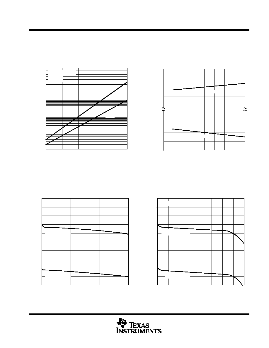
TLE206x, TLE206xA, TLE206xB, TLE206xY
EXCALIBUR JFET-INPUT HIGH-OUTPUT-DRIVE
µ
POWER OPERATIONAL AMPLIFIERS
SLOS193A ≠ FEBRUARY 1997 ≠ REVISED MARCH 1998
51
POST OFFICE BOX 655303
∑
DALLAS, TEXAS 75265
TYPICAL CHARACTERISTICS
Figure 8
INPUT BIAS CURRENT
AND INPUT OFFSET CURRENT
vs
FREE-AIR TEMPERATURE
TA ≠ Free-Air Temperature ≠
∞
C
105
85
65
45
25
105
104
103
102
101
100
VIC = 0
VCC
±
=
±
15 V
≠ Input Bias and Input Offset Currents ≠ pA
I IB
and I
IO
ŒŒ
ŒŒ
IIO
ŒŒ
ŒŒ
IIB
125
Figure 9
COMMON-MODE INPUT VOLTAGE
vs
FREE-AIR TEMPERATURE
125
100
75
50
25
0
≠ 25
≠ 50
≠ 75
TA ≠ Free-Air Temperature ≠
∞
C
VCC +
VCC +
VCC ≠
VCC ≠
VCC ≠ + 2
+ 3
+ 4
VCC +
+ 1
+ 2
≠ Common-Mode Input V
oltage ≠ V
V
IC
ŒŒŒ
VIC +
ŒŒ
ŒŒ
VIC ≠
Figure 10
MAXIMUM POSITIVE PEAK
OUTPUT VOLTAGE
vs
OUTPUT CURRENT
≠ Maximum Positive Peak Output V
oltage ≠ V
V
OM+
≠ 60
≠ 50
≠ 40
≠ 30
≠ 20
≠ 10
0
IO ≠ Output Current ≠ mA
0
2
4
6
8
10
12
14
16
18
20
VCC
±
=
±
5 V
VCC
±
=
±
15 V
ŒŒŒŒŒ
ŒŒŒŒŒ
TA = 25
∞
C
Figure 11
MAXIMUM NEGATIVE PEAK
OUTPUT VOLTAGE
vs
OUTPUT CURRENT
≠ Maximum Negative Peak Output V
oltage ≠ V
V
OM
≠
30
35
VCC
±
=
±
15 V
VCC
±
=
±
5 V
IO ≠ Output Current ≠ mA
0
5
10
15
20
25
40
≠ 20
≠ 18
≠ 16
≠ 14
≠ 12
≠ 10
≠ 8
≠ 6
≠ 4
≠ 2
0
ŒŒŒŒ
ŒŒŒŒ
TA = 25
∞
C
Data at high and low temperatures are applicable only within the rated operating free-air temperature ranges of the various devices.
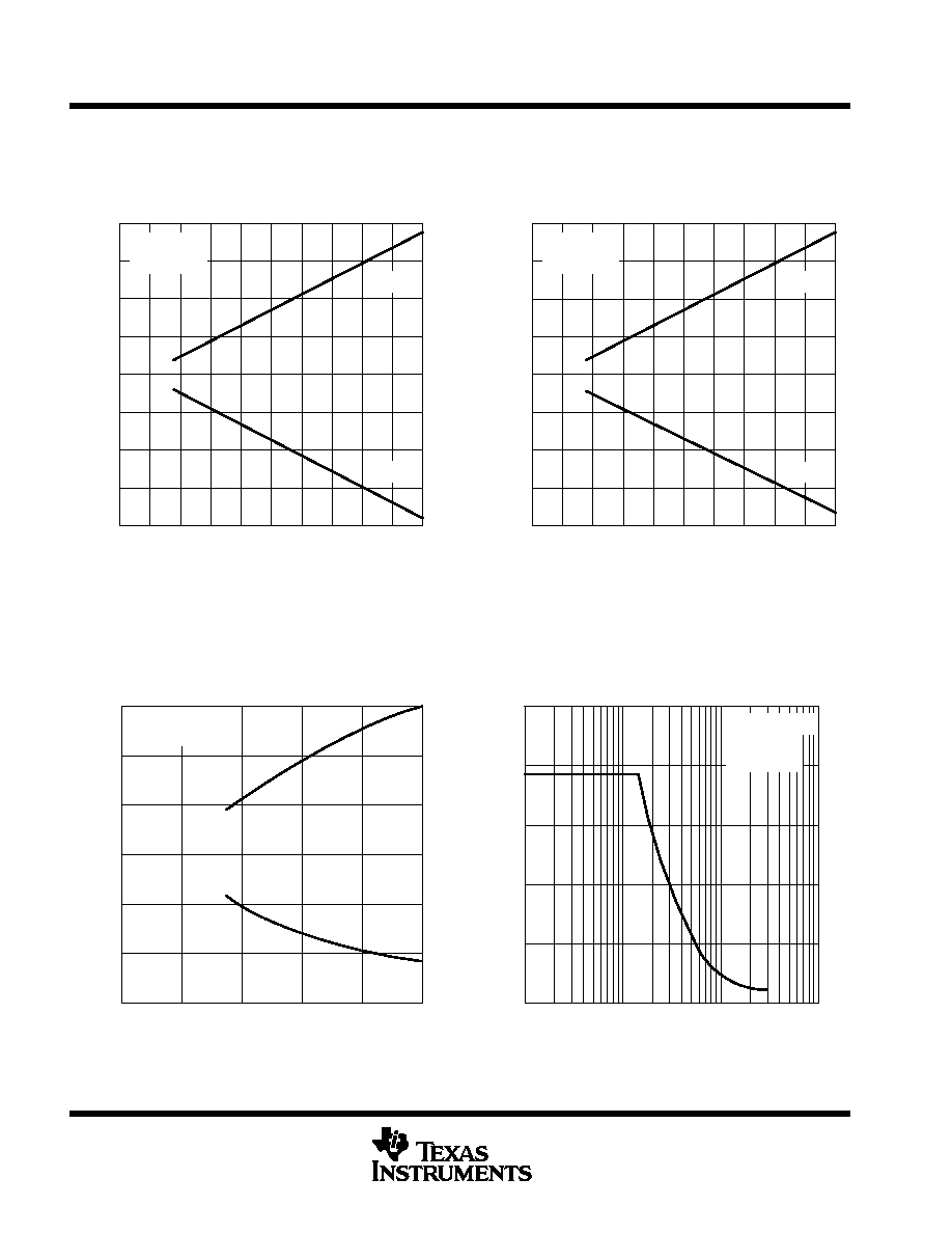
TLE206x, TLE206xA, TLE206xB, TLE206xY
EXCALIBUR JFET-INPUT HIGH-OUTPUT-DRIVE
µ
POWER OPERATIONAL AMPLIFIERS
SLOS193A ≠ FEBRUARY 1997 ≠ REVISED MARCH 1998
52
POST OFFICE BOX 655303
∑
DALLAS, TEXAS 75265
TYPICAL CHARACTERISTICS
Figure 12
MAXIMUM PEAK OUTPUT VOLTAGE
vs
SUPPLY VOLTAGE
≠ Maximum Peak Output V
oltage ≠ V
V
OM
20
18
16
14
12
10
8
6
4
2
0
| VCC
±
| ≠ Supply Voltage ≠ V
≠ 20
≠ 15
≠ 10
≠ 5
0
5
10
15
20
VOM ≠
VOM +
TA = 25
∞
C
RL = 10 k
Figure 13
MAXIMUM PEAK OUTPUT VOLTAGE
vs
SUPPLY VOLTAGE
RL = 600
TA = 25
∞
C
VOM +
VOM ≠
20
15
10
5
0
≠ 5
≠ 10
≠ 15
≠ 20
| VCC
+
| ≠ Supply Voltage ≠ V
0
2
4
6
8
10
12
14
16
18
20
≠ Maximum Peak Output V
oltage ≠ V
V
OM
Figure 14
MAXIMUM PEAK OUTPUT VOLTAGE
vs
SUPPLY VOLTAGE
≠ Maximum Peak Output V
oltage ≠ V
V
OM
VOM ≠
VOM +
TA = 25
∞
C
RL = 100
10
8
6
4
2
0
| VCC
±
|
≠ Supply Voltage ≠ V
≠ 6
≠ 4
≠ 2
0
2
4
6
Figure 15
MAXIMUM PEAK-TO-PEAK
OUTPUT VOLTAGE
vs
FREQUENCY
≠ Maximum Peak-to-Peak Output V
oltage ≠ V
V
O(PP)
TA = 25
∞
C
RL = 10 k
VCC
±
=
±
5 V
10
8
6
10 k
100 k
1 M
10 M
f ≠ Frequency ≠ Hz
4
2
0
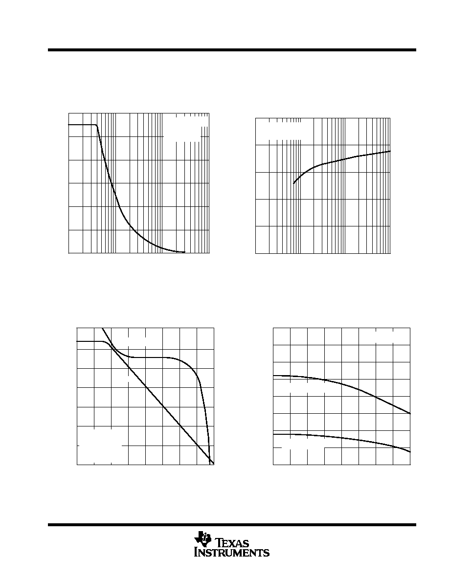
TLE206x, TLE206xA, TLE206xB, TLE206xY
EXCALIBUR JFET-INPUT HIGH-OUTPUT-DRIVE
µ
POWER OPERATIONAL AMPLIFIERS
SLOS193A ≠ FEBRUARY 1997 ≠ REVISED MARCH 1998
53
POST OFFICE BOX 655303
∑
DALLAS, TEXAS 75265
TYPICAL CHARACTERISTICS
Figure 16
≠ Maximum Peak-to-Peak Output V
oltage ≠ V
V
O(PP)
MAXIMUM PEAK-TO-PEAK
OUTPUT VOLTAGE
vs
FREQUENCY
15
RL = 10 k
VCC
±
=
±
15 V
30
25
20
10 k
100 k
1 M
10 M
f ≠ Frequency ≠ Hz
10
5
0
ŒŒŒŒ
ŒŒŒŒ
TA = 25
∞
C
Figure 17
MAXIMUM PEAK-TO-PEAK
OUTPUT VOLTAGE
vs
LOAD RESISTANCE
RL ≠ Load Resistance ≠
10 k
1 k
100
10
0
2
4
6
8
10
ŒŒŒŒŒŒ
ŒŒŒŒŒŒ
ŒŒŒŒŒŒ
VCC
±
=
±
5 V
TA = 25
∞
C
≠ Maximum Peak-to-Peak Output V
oltage ≠ V
V
O(PP)
≠ Large-Signal DIfferential V
oltage
Amplification ≠ dB
A
VD
LARGE-SIGNAL DIFFERENTIAL VOLTAGE
AMPLIFICATION AND PHASE SHIFT
vs
FREQUENCY
Phase Shift
TA = 25
∞
C
CL = 100 pF
RL = 10 k
VCC
±
=
±
15 V
Phase Shift
60
∞
80
∞
100
∞
120
∞
140
∞
160
∞
180
∞
200
∞
10 M
1 M
100 k
10 k
1 k
100
10
1
0.1
f ≠ Frequency ≠ Hz
≠20
0
20
40
60
80
100
120
ŒŒ
AVD
Figure 18
LARGE-SIGNAL VOLTAGE AMPLIFICATION
vs
FREE-AIR TEMPERATURE
RL = 10 k
VCC
±
=
±
5 V
VCC
±
=
±
15 V
TA ≠ Free-Air Temperature ≠
∞
C
125
100
75
50
25
0
≠ 25
≠ 50
≠ 75
350
300
250
200
150
100
50
0
400
≠ Large-Signal DIfferential V
oltage
Amplification ≠ V/mV
A
VD
Figure 19
Data at high and low temperatures are applicable only within the rated operating free-air temperature ranges of the various devices.
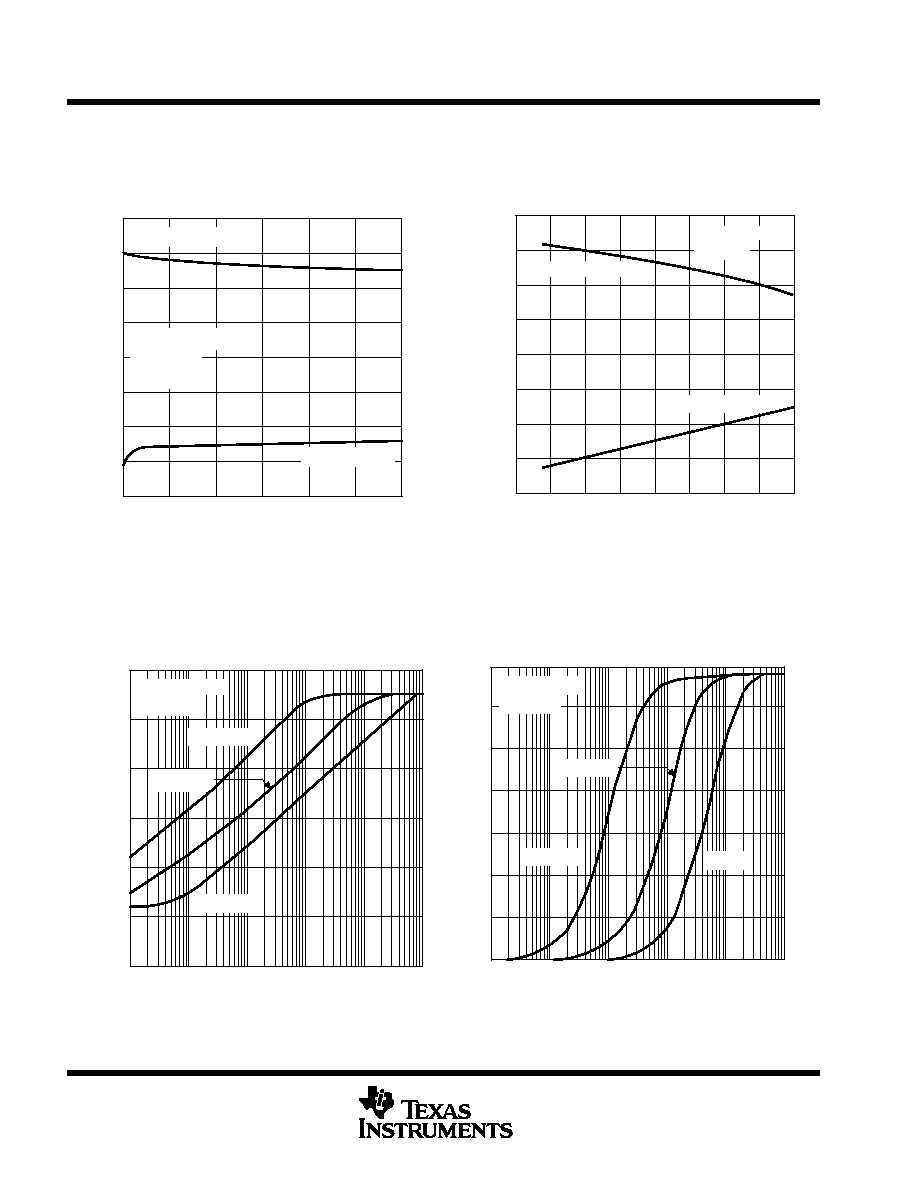
TLE206x, TLE206xA, TLE206xB, TLE206xY
EXCALIBUR JFET-INPUT HIGH-OUTPUT-DRIVE
µ
POWER OPERATIONAL AMPLIFIERS
SLOS193A ≠ FEBRUARY 1997 ≠ REVISED MARCH 1998
54
POST OFFICE BOX 655303
∑
DALLAS, TEXAS 75265
TYPICAL CHARACTERISTICS
Figure 20
≠ Short-Circuit Output Current ≠ mA
I OS
SHORT-CIRCUIT OUTPUT CURRENT
vs
ELAPSED TIME
VID = 100 mV
VO = 0
TA = 25
∞
C
VCC
±
=
±
15 V
VID = ≠ 100 mV
60
50
40
30
20
10
0
t ≠ Elapsed Time ≠ s
≠ 80
≠ 60
≠ 40
≠ 20
0
20
40
60
80
Figure 21
SHORT-CIRCUIT OUTPUT CURRENT
vs
FREE-AIR TEMPERATURE
VID = ≠ 100 mV
VID = 100 mV
VO = 0
VCC
±
=
±
15 V
80
≠ 80
≠ 60
≠ 40
≠ 20
0
20
40
60
≠ 75
≠ 50
≠ 25
0
25
50
75
100
125
TA ≠ Free-Air Temperature ≠
∞
C
≠ Short-Circuit Output Current ≠ mA
I OS
Figure 22
TA = 25
∞
C
VCC
±
=
±
15 V
AVD = 10
f ≠ Frequency ≠ Hz
1 M
100 k
10 k
1 k
100
10
≠ Output Impedance ≠
0.001
0.01
0.1
1
10
100
1000
¡¡
¡¡
z
o
¡¡
¡¡
AVD = 100
ŒŒŒ
ŒŒŒ
AVD = 1
TLE2061
OUTPUT IMPEDANCE
vs
FREQUENCY
Figure 23
≠ Output Impedance ≠
z
o
35
30
25
20
15
10
5
TA = 25
∞
C
VCC
±
=
±
15 V
AVD = 100
f ≠ Frequency ≠ Hz
1 M
100 k
10 k
1 k
100
0
ŒŒŒ
ŒŒŒ
AVD = 1
ŒŒŒ
AVD = 10
10 M
TLE2062 AND TLE2064
OUTPUT IMPEDANCE
vs
FREQUENCY
Data at high and low temperatures are applicable only within the rated operating free-air temperature ranges of the various devices.
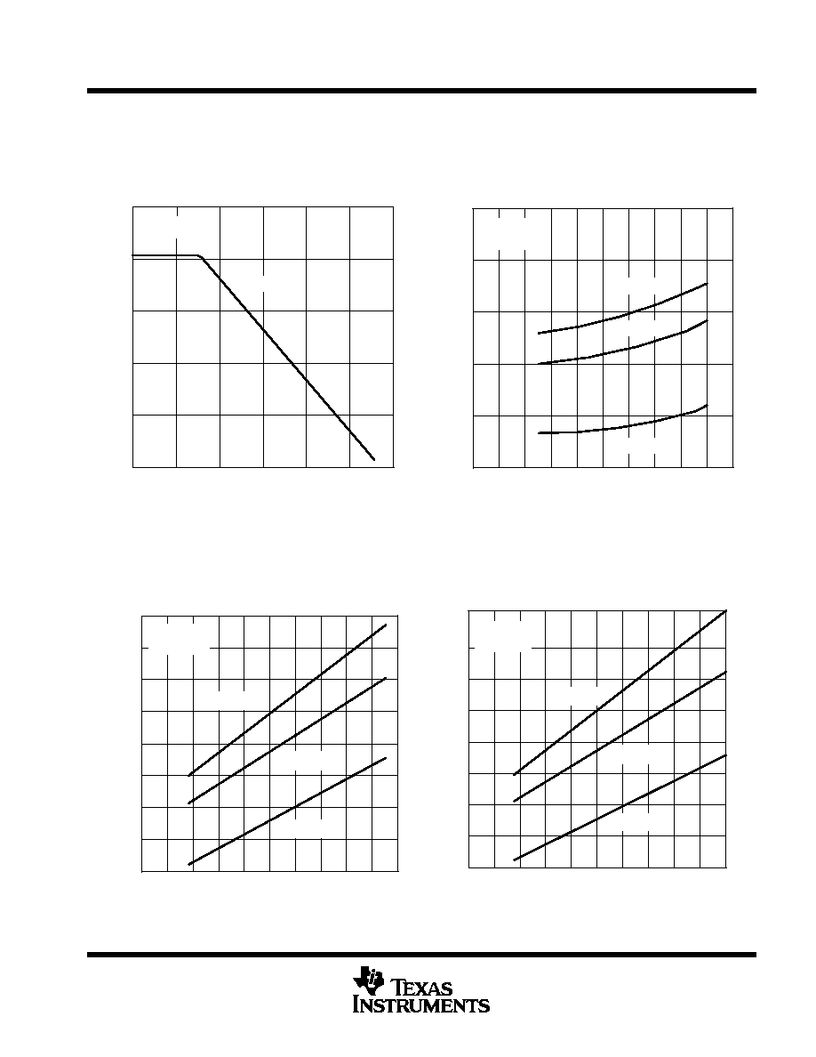
TLE206x, TLE206xA, TLE206xB, TLE206xY
EXCALIBUR JFET-INPUT HIGH-OUTPUT-DRIVE
µ
POWER OPERATIONAL AMPLIFIERS
SLOS193A ≠ FEBRUARY 1997 ≠ REVISED MARCH 1998
55
POST OFFICE BOX 655303
∑
DALLAS, TEXAS 75265
TYPICAL CHARACTERISTICS
Figure 24
COMMON-MODE REJECTION RATIO
vs
FREQUENCY
CMRR ≠ Common-Mode Rejection Ratio ≠ dB
10
100
1 k
10 k
100 k
1 M
f ≠ Frequency ≠ Hz
10 M
0
20
40
60
80
100
TA = 25
∞
C
ŒŒŒŒŒ
ŒŒŒŒŒ
VCC
±
=
±
5 V
Figure 25
A
µ
2
≠ Supply Current ≠
I CC
No Load
VO = 0
TA = 125
∞
C
TA = 25
∞
C
TA = ≠ 55
∞
C
20
18
16
14
12
10
8
6
4
0
| VCC
±
| ≠ Supply Voltage ≠ V
340
240
260
280
300
320
TLE2061
SUPPLY CURRENT
vs
SUPPLY VOLTAGE
Figure 26
|VCC
±
| ≠ Supply Voltage ≠ V
ICC ≠ Supply Current ≠ xA CC
I
600
575
525
500
0
2
4
6
8
10
12
625
675
700
14
16
18
20
550
650
A
µ
TA = 25
∞
C
TA = 125
∞
C
TA = ≠ 55
∞
C
VO = 0
No Load
TLE2062
SUPPLY CURRENT
vs
SUPPLY VOLTAGE
Figure 27
≠ Supply Current ≠ mA
I CC
1
1.1
1.2
1.3
1.4
No Load
VO = 0
TA = 125
∞
C
TA = 25
∞
C
TA = ≠ 55
∞
C
| VCC
±
| ≠ Supply Voltage ≠ V
20
18
16
14
12
10
8
6
4
2
0
1.25
1.35
1.05
1.15
TLE2064
SUPPLY CURRENT
vs
SUPPLY VOLTAGE
Data at high and low temperatures are applicable only within the rated operating free-air temperature ranges of the various devices.
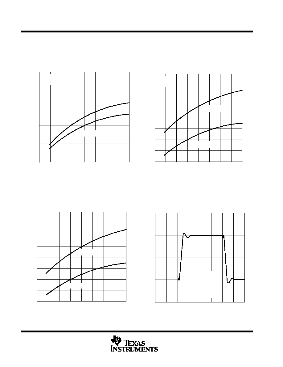
TLE206x, TLE206xA, TLE206xB, TLE206xY
EXCALIBUR JFET-INPUT HIGH-OUTPUT-DRIVE
µ
POWER OPERATIONAL AMPLIFIERS
SLOS193A ≠ FEBRUARY 1997 ≠ REVISED MARCH 1998
56
POST OFFICE BOX 655303
∑
DALLAS, TEXAS 75265
TYPICAL CHARACTERISTICS
Figure 28
A
µ
≠75
≠ Supply Current ≠
I CC
VCC
±
=
±
5 V
VO = 0
No Load
240
260
280
300
320
340
125
100
75
50
25
0
≠ 25
≠ 50
TA ≠ Free-Air Temperature ≠
∞
C
260
280
300
ŒŒŒŒŒ
ŒŒŒŒŒ
VCC
±
=
±
15 V
TLE2061
SUPPLY CURRENT
vs
FREE-AIR TEMPERATURE
Figure 29
≠ 75 ≠ 50
≠ 25
0
25
50
75
100
125
VCC
±
=
±
5 V
VCC
±
=
±
15 V
VO = 0
No Load
600
575
525
500
625
675
700
550
650
TA ≠ Free-Air Temperature ≠
∞
C
ICC ≠ Supply Current ≠ xA CC
I
A
µ
TLE2062
SUPPLY CURRENT
vs
FREE-AIR TEMPERATURE
Figure 30
≠ Supply Current ≠ mA
I CC
1.4
1.3
1.2
1.1
ŒŒŒŒŒ
ŒŒŒŒŒ
VCC
±
=
±
5 V
ŒŒŒŒŒ
VCC
±
=
±
15 V
VO = 0
No Load
TA ≠ Free-Air Temperature ≠
∞
C
1
125
100
75
50
25
0
≠ 25
≠ 50
≠ 75
1.25
1.35
1.05
1.15
TLE2064
SUPPLY CURRENT
vs
FREE-AIR TEMPERATURE
Figure 31
≠ Output V
oltage
≠
mV
V
O
VOLTAGE-FOLLOWER
SMALL-SIGNAL
PULSE RESPONSE
t ≠ Time ≠
µ
s
2
1
0
≠ 100
≠ 50
0
50
100
VCC
±
=
±
5 V
RL = 10 k
CL = 100 pF
TA = 25
∞
C
See Figure 1
2.5
1.5
0.5
Data at high and low temperatures are applicable only within the rated operating free-air temperature ranges of the various devices.
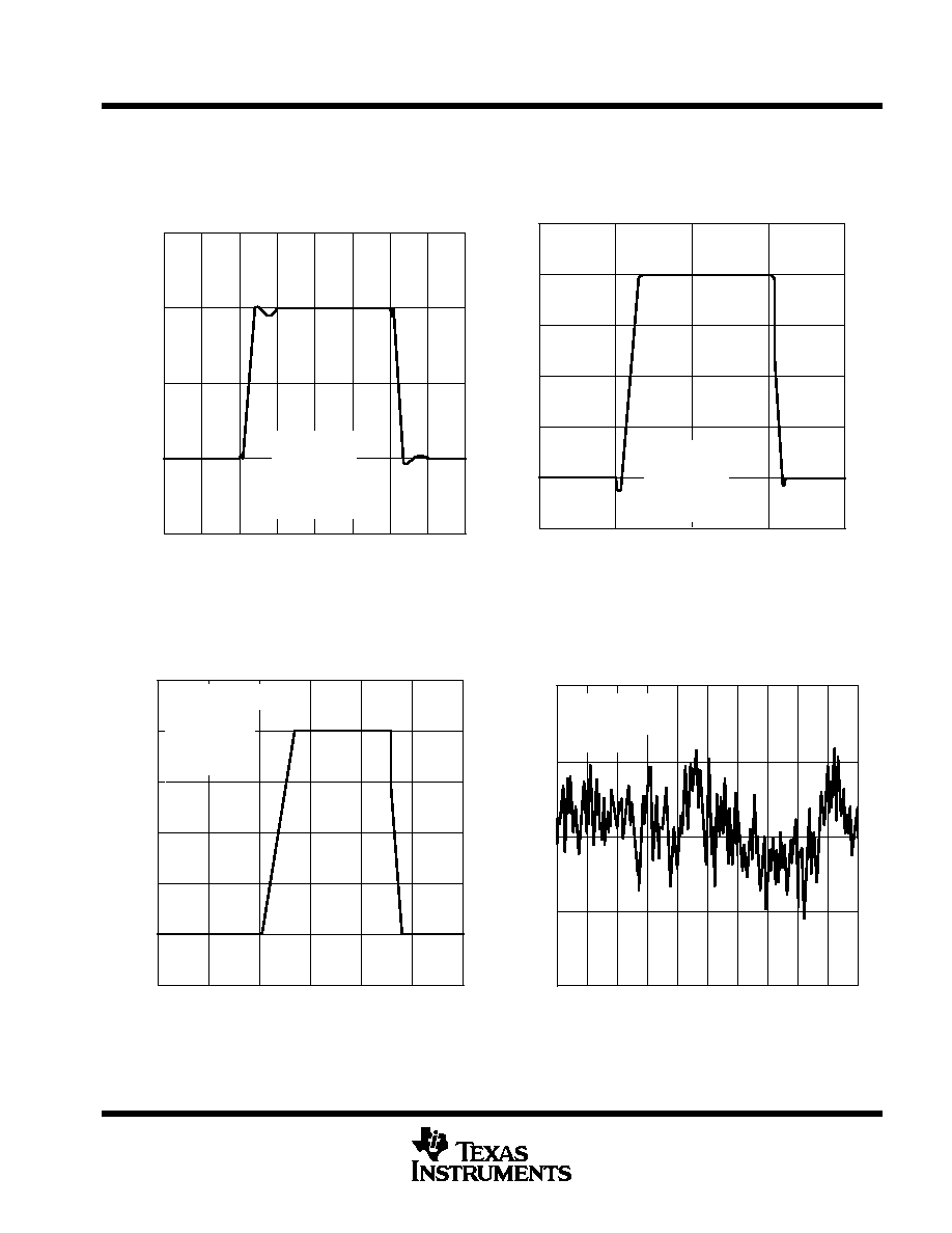
TLE206x, TLE206xA, TLE206xB, TLE206xY
EXCALIBUR JFET-INPUT HIGH-OUTPUT-DRIVE
µ
POWER OPERATIONAL AMPLIFIERS
SLOS193A ≠ FEBRUARY 1997 ≠ REVISED MARCH 1998
57
POST OFFICE BOX 655303
∑
DALLAS, TEXAS 75265
TYPICAL CHARACTERISTICS
Figure 32
3
≠ Output V
oltage
≠
mV
V
O
VOLTAGE-FOLLOWER
SMALL-SIGNAL
PULSE RESPONSE
100
50
0
≠ 50
≠ 100
0
1
2
3
t ≠ Time ≠
µ
s
VCC
±
=
±
15 V
RL = 10 k
CL = 100 pF
TA = 25
∞
C
See Figure 1
2.5
1.5
0.5
Figure 33
VOLTAGE-FOLLOWER
LARGE-SIGNAL
PULSE RESPONSE
0
5
10
15
t ≠ Time ≠
µ
s
≠ 2
≠ 1
0
1
2
3
4
≠ Output V
oltage ≠ V
V
O
ŒŒŒŒŒ
ŒŒŒŒŒ
ŒŒŒŒŒ
ŒŒŒŒŒ
VCC
±
=
±
5 V
RL = 10 k
CL = 100 pF
TA = 25
∞
C
See Figure 1
Figure 34
≠ Output V
oltage ≠ V
V
O
VOLTAGE-FOLLOWER
LARGE-SIGNAL
PULSE RESPONSE
t ≠ Time ≠
µ
s
40
30
20
10
0
≠ 15
≠ 10
≠ 5
0
5
10
15
VCC
±
=
±
15 V
RL = 10 k
CL = 100 pF
TA = 25
∞
C
See Figure 1
Figure 35
NOISE VOLTAGE
(REFERRED TO INPUT)
0.1 TO 10 Hz
t ≠ Time ≠
µ
s
Noise V
oltage ≠ V
10
9
8
7
6
5
4
3
2
1
0
≠ 1
≠ 0.5
0
0.5
1
TA = 25
∞
C
VCC
±
=
±
15 V
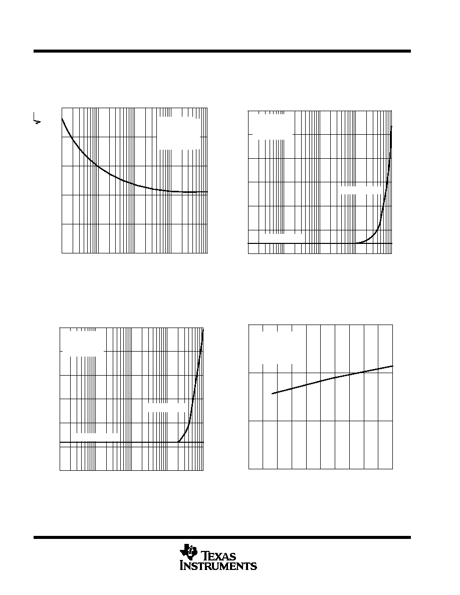
TLE206x, TLE206xA, TLE206xB, TLE206xY
EXCALIBUR JFET-INPUT HIGH-OUTPUT-DRIVE
µ
POWER OPERATIONAL AMPLIFIERS
SLOS193A ≠ FEBRUARY 1997 ≠ REVISED MARCH 1998
58
POST OFFICE BOX 655303
∑
DALLAS, TEXAS 75265
TYPICAL CHARACTERISTICS
Figure 36
≠ Equivalent Input Noise V
oltage ≠
V
n
EQUIVALENT INPUT NOISE VOLTAGE
vs
FREQUENCY
10 k
1 k
100
10
1
f ≠ Frequency ≠ Hz
0
20
40
60
80
100
nV/
Hz
ŒŒŒŒŒ
ŒŒŒŒŒ
ŒŒŒŒŒ
VCC
±
=
±
5 V
RS = 20
TA = 25
∞
C
See Figure 2
Figure 37
TOTAL HARMONIC DISTORTION
vs
FREQUENCY
VCC
±
=
±
5 V
AVD = 2
VO(PP) = 2 V
TA = 25
∞
C
Source Signal
0.2
0.1
100 k
10 k
1 k
100
10
f ≠ Frequency ≠ Hz
THD
≠
T
otal Harmonic Distortion ≠ %
0
0.3
Figure 38
TOTAL HARMONIC DISTORATION
vs
FREQUENCY
VCC
±
=
±
5 V
Source Signal
TA = 25
∞
C
VO(PP) = 2 V
AVD = 10
0.3
0.1
0.5
0.6
0
THD
≠
T
otal Harmonic Distortion ≠ %
f ≠ Frequency ≠ Hz
10
100
1 k
10 k
100 k
0.2
0.4
Figure 39
UNITY-GAIN BANDWIDTH
vs
SUPPLY VOLTAGE
See Figure 3
TA = 25
∞
C
CL = 100 pF
RL = 10 k
20
18
16
14
12
10
8
6
4
2
| VCC
±
| ≠ Supply Voltage ≠ V
2.5
2
1.5
1
0
≠ Unity-Gain Bandwidth ≠ MHz
B
1
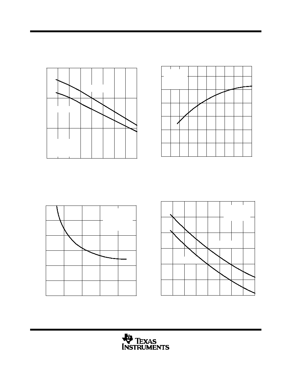
TLE206x, TLE206xA, TLE206xB, TLE206xY
EXCALIBUR JFET-INPUT HIGH-OUTPUT-DRIVE
µ
POWER OPERATIONAL AMPLIFIERS
SLOS193A ≠ FEBRUARY 1997 ≠ REVISED MARCH 1998
59
POST OFFICE BOX 655303
∑
DALLAS, TEXAS 75265
TYPICAL CHARACTERISTICS
Figure 40
UNITY-GAIN BANDWIDTH
vs
FREE-AIR TEMPERATURE
RL = 10 k
CL = 100 pF
See Figure 3
VCC
±
=
±
5 V
VCC
±
=
±
15 V
TA ≠ Free-Air Temperature ≠
∞
C
125
100
75
50
25
0
≠ 25
≠ 50
≠ 75
1
1.5
2
2.5
≠ Unity-Gain Bandwidth ≠ MHz
B
1
Figure 41
PHASE MARGIN
vs
SUPPLY VOLTAGE
RL = 10 k
CL = 100 pF
TA = 25
∞
C
See Figure 3
62
∞
61
∞
60
∞
59
∞
58
∞
57
∞
56
∞
0
| VCC
±
| ≠ Supply Voltage ≠ V
2
4
6
8
10
12
14
16
18
20
55
∞
≠ Phase Margin
¡¡
¡¡
m
Figure 42
PHASE MARGIN
vs
LOAD CAPACITANCE
CL ≠ Load Capacitance ≠ pF
1000
800
600
400
200
0
10
∞
20
∞
30
∞
40
∞
50
∞
0
∞
60
∞
See Figure 3
TA = 25
∞
C
RL = 10 k
VCC
±
=
±
15 V
≠ Phase Margin
¡¡
¡¡
m
Figure 43
PHASE MARGIN
vs
FREE-AIR TEMPERATURE
≠ Phase Margin
¡¡
¡¡
m
125
100
75
50
25
0
≠ 25
≠ 50
≠ 75
TA ≠ Free-Air Temperature ≠
∞
C
54
∞
56
∞
58
∞
60
∞
62
∞
64
∞
66
∞
VCC
±
=
±
5 V
VCC
±
=
±
15 V
See Figure 3
CL = 100 pF
RL = 10 k
Data at high and low temperatures are applicable only within the rated operating free-air temperature ranges of the various devices.
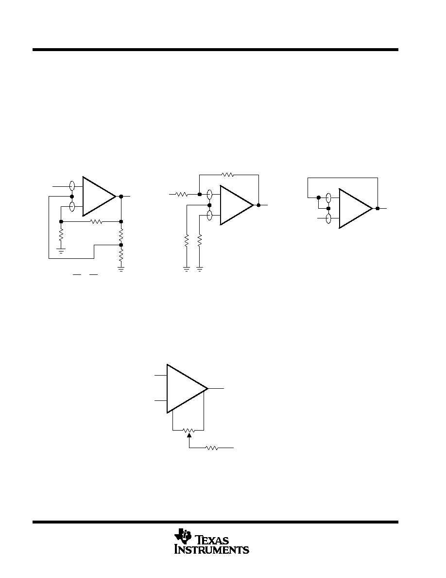
TLE206x, TLE206xA, TLE206xB, TLE206xY
EXCALIBUR JFET-INPUT HIGH-OUTPUT-DRIVE
µ
POWER OPERATIONAL AMPLIFIERS
SLOS193A ≠ FEBRUARY 1997 ≠ REVISED MARCH 1998
60
POST OFFICE BOX 655303
∑
DALLAS, TEXAS 75265
APPLICATION INFORMATION
input characteristics
The TLE206x, TLE206xA, and TLE206xB are specified with a minimum and a maximum input voltage that if
exceeded at either input could cause the device to malfunction. Because of the extremely high input impedance
and resulting low bias current requirements, the TLE206x, TLE206xA, and TLE206xB are well suited for
low-level signal processing; however, leakage currents on printed-circuit boards and sockets can easily exceed
bias current requirements and cause degradation in system performance. It is good practice to include guard
rings around inputs (see Figure 44). These guards should be driven from a low-impedance source at the same
voltage level as the common-mode input.
VI
R2
R1
VI
R4
+
≠
VO
R3
VI
+
≠
VO
VO
+
≠
R3
R4
+
R2
R1
Where
Figure 44. Use of Guard Rings
TLE2061 input offset voltage nulling
The TLE2061 series offers external null pins that can be used to further reduce the input offset voltage. The
circuit of Figure 45 can be connected as shown if the feature is desired. When external nulling is not needed,
the null pins may be left unconnected.
+
≠
VCC ≠
N2
N1
100 k
5 k
IN ≠
IN +
OUT
Figure 45. Input Offset Voltage Nulling
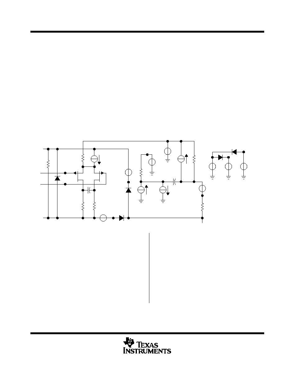
TLE206x, TLE206xA, TLE206xB, TLE206xY
EXCALIBUR JFET-INPUT HIGH-OUTPUT-DRIVE
µ
POWER OPERATIONAL AMPLIFIERS
SLOS193A ≠ FEBRUARY 1997 ≠ REVISED MARCH 1998
61
POST OFFICE BOX 655303
∑
DALLAS, TEXAS 75265
APPLICATION INFORMATION
macromodel information
Macromodel information provided was derived using Microsim
Parts
TM
, the model generation software used
with Microsim
PSpice
TM
. The Boyle macromodel (see Note 5) and subcircuit in Figure 46 were generated using
the TLE206x typical electrical and operating characteristics at 25
∞
C. Using this information, output simulations
of the following key parameters can be generated to a tolerance of 20% (in most cases):
D
Unity-gain frequency
D
Common-mode rejection ratio
D
Phase margin
D
DC output resistance
D
AC output resistance
D
Short-circuit output current limit
D
Maximum positive output voltage swing
D
Maximum negative output voltage swing
D
Slew rate
D
Quiescent power dissipation
D
Input bias current
D
Open-loop voltage amplification
NOTE 5: G. R. Boyle, B. M. Cohn, D. O. Pederson, and J. E. Solomon, "
Macromodeling of Integrated Circuit Operational Amplifiers", IEEE Journal
of Solid-State Circuits, SC-9, 353 (1974).
OUT
+
≠
+
≠
+
≠
+
≠
+
≠
+
≠
+
≠
+
≠
.subckt TLE2062 1 2 3 4 5
c1
11
12 1.457E≠12
c2
6
7 15.00E≠12
dc
5
53 dx
de
54
5 dx
dlp
90
91 dx
dln
92
90 dx
dp
4
3 dx
egnd 99
0 poly (2) (3,0) (4,0) 0 .5 .5
fb
7
99 poly (5) vb vc ve vlp
+ vln 0 4.357E6 ≠ 4E6 4E6 4E6 ≠ 4E6
ga
6
0 11 12 188.5E≠6
gcm
0
6 10 99 3.352E≠9
iss
3
10 dc 51.00E≠6
hlim 90
0 vlim 1k
j1
11
2 10 jx
j2
12
1 10 jx
r2
6
9 100.0E3
VCC +
rp
IN ≠
2
IN+
1
VCC ≠
rd1
11
j1
j2
10
rss
iss
3
12
rd2
ve
54
de
dp
vc
dc
4
C1
53
r2
6
9
egnd
vb
fb
C2
gcm
ga
vlim
8
5
ro1
ro2
hlim
90
dip
91
din
92
vin
vip
99
7
rd1
4
11 5.305E3
rd2
4
12 5.305E3
r01
8
5 280
r02
7
99 280
rp
3
4 113.2E3
rss
10
99 3.922E6
vb
9
0 dc 0
vc
3
53 dc 2
ve
54
4 dc 2
vlim 7
8 dc 0
vlp
91
0
dc 50
vln
0
92 dc 50
.model dx D(Is=800.0E≠18)
.model jx PJF(Is=2.000E≠12 Beta = 423E≠6
+ Vto = ≠ 1)
.ends
Figure 46. Boyle Macromodel and Subcircuit
PSpice and Parts are trademarks of MicroSim Corporation.
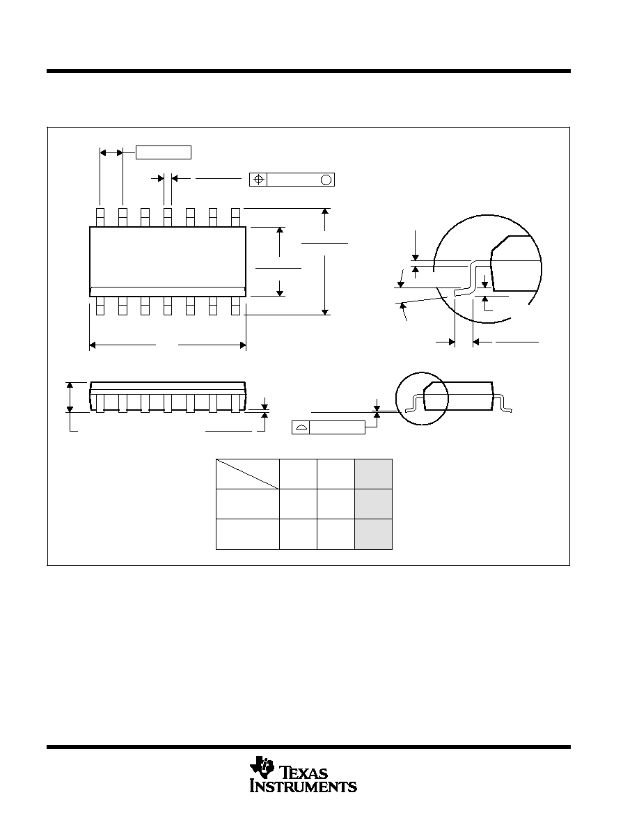
TLE206x, TLE206xA, TLE206xB, TLE206xY
EXCALIBUR JFET-INPUT HIGH-OUTPUT-DRIVE
µ
POWER OPERATIONAL AMPLIFIERS
SLOS193A ≠ FEBRUARY 1997 ≠ REVISED MARCH 1998
62
POST OFFICE BOX 655303
∑
DALLAS, TEXAS 75265
MECHANICAL INFORMATION
D (R-PDSO-G**)
PLASTIC SMALL-OUTLINE PACKAGE
14 PIN SHOWN
4040047 / D 10/96
0.228 (5,80)
0.244 (6,20)
0.069 (1,75) MAX
0.010 (0,25)
0.004 (0,10)
1
14
0.014 (0,35)
0.020 (0,51)
A
0.157 (4,00)
0.150 (3,81)
7
8
0.044 (1,12)
0.016 (0,40)
Seating Plane
0.010 (0,25)
PINS **
0.008 (0,20) NOM
A MIN
A MAX
DIM
Gage Plane
0.189
(4,80)
(5,00)
0.197
8
(8,55)
(8,75)
0.337
14
0.344
(9,80)
16
0.394
(10,00)
0.386
0.004 (0,10)
M
0.010 (0,25)
0.050 (1,27)
0
∞
≠ 8
∞
NOTES: A. All linear dimensions are in inches (millimeters).
B. This drawing is subject to change without notice.
C. Body dimensions do not include mold flash or protrusion, not to exceed 0.006 (0,15).
D. Falls within JEDEC MS-012
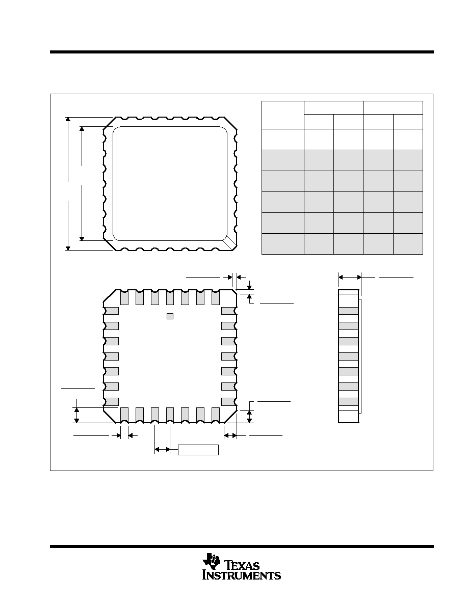
TLE206x, TLE206xA, TLE206xB, TLE206xY
EXCALIBUR JFET-INPUT HIGH-OUTPUT-DRIVE
µ
POWER OPERATIONAL AMPLIFIERS
SLOS193A ≠ FEBRUARY 1997 ≠ REVISED MARCH 1998
63
POST OFFICE BOX 655303
∑
DALLAS, TEXAS 75265
MECHANICAL INFORMATION
FK (S-CQCC-N**)
LEADLESS CERAMIC CHIP CARRIER
4040140 / D 10/96
28 TERMINAL SHOWN
B
0.358
(9,09)
MAX
(11,63)
0.560
(14,22)
0.560
0.458
0.858
(21,8)
1.063
(27,0)
(14,22)
A
NO. OF
MIN
MAX
0.358
0.660
0.761
0.458
0.342
(8,69)
MIN
(11,23)
(16,26)
0.640
0.739
0.442
(9,09)
(11,63)
(16,76)
0.962
1.165
(23,83)
0.938
(28,99)
1.141
(24,43)
(29,59)
(19,32)
(18,78)
**
20
28
52
44
68
84
0.020 (0,51)
TERMINALS
0.080 (2,03)
0.064 (1,63)
(7,80)
0.307
(10,31)
0.406
(12,58)
0.495
(12,58)
0.495
(21,6)
0.850
(26,6)
1.047
0.045 (1,14)
0.045 (1,14)
0.035 (0,89)
0.035 (0,89)
0.010 (0,25)
12
13
14
15
16
18
17
11
10
8
9
7
5
4
3
2
0.020 (0,51)
0.010 (0,25)
6
1
28
26
27
19
21
B SQ
A SQ
22
23
24
25
20
0.055 (1,40)
0.045 (1,14)
0.028 (0,71)
0.022 (0,54)
0.050 (1,27)
NOTES: A. All linear dimensions are in inches (millimeters).
B. This drawing is subject to change without notice.
C. This package can be hermetically sealed with a metal lid.
D. The terminals are gold plated.
E. Falls within JEDEC MS-004
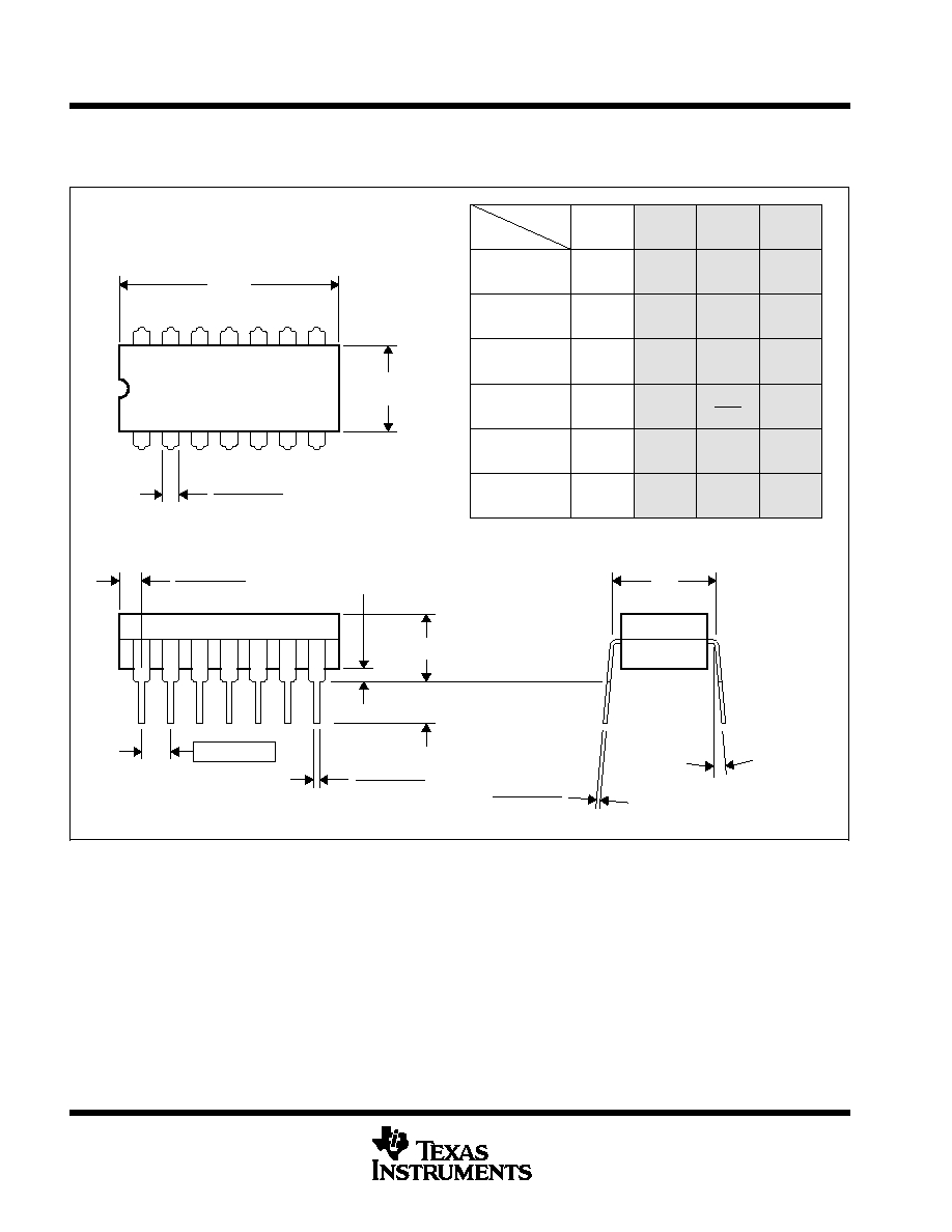
TLE206x, TLE206xA, TLE206xB, TLE206xY
EXCALIBUR JFET-INPUT HIGH-OUTPUT-DRIVE
µ
POWER OPERATIONAL AMPLIFIERS
SLOS193A ≠ FEBRUARY 1997 ≠ REVISED MARCH 1998
64
POST OFFICE BOX 655303
∑
DALLAS, TEXAS 75265
MECHANICAL INFORMATION
J (R-GDIP-T**)
CERAMIC DUAL-IN-LINE PACKAGE
14 PIN SHOWN
20
0.290
(7,87)
0.310
0.975
(24,77)
(23,62)
0.930
(7,37)
0.245
(6,22)
(7,62)
0.300
18
16
14
PINS **
0.290
(7,87)
0.310
0.785
(19,94)
(19,18)
0.755
(7,37)
0.310
(7,87)
(7,37)
0.290
0.755
(19,18)
(19,94)
0.785
0.245
(6,22)
(7,11)
0.280
A
0.300
(7,62)
(6,22)
0.245
A MIN
A MAX
B MAX
B MIN
C MIN
C MAX
DIM
0.310
(7,87)
(7,37)
0.290
(23,10)
0.910
0.300
(7,62)
(6,22)
0.245
Seating Plane
0.014 (0,36)
0.008 (0,20)
4040083/C 08/96
C
8
7
0.020 (0,51) MIN
B
0.070 (1,78)
0.100 (2,54)
0.065 (1,65)
0.045 (1,14)
14
1
0.015 (0,38)
0.023 (0,58)
0.200 (5,08) MAX
0.130 (3,30) MIN
0.100 (2,54)
0
∞
≠ 15
∞
NOTES: A. All linear dimensions are in inches (millimeters).
B. This drawing is subject to change without notice.
C. This package can be hermetically sealed with a ceramic lid using glass frit.
D. Index point is provided on cap for terminal identification only on press ceramic glass frit seal only.
E. Falls within MIL-STD-1835 GDIP1-T14, GDIP1-T16, GDIP1-T18, and GDIP1-T20
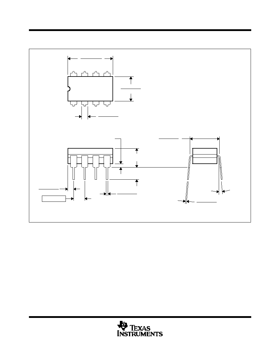
TLE206x, TLE206xA, TLE206xB, TLE206xY
EXCALIBUR JFET-INPUT HIGH-OUTPUT-DRIVE
µ
POWER OPERATIONAL AMPLIFIERS
SLOS193A ≠ FEBRUARY 1997 ≠ REVISED MARCH 1998
65
POST OFFICE BOX 655303
∑
DALLAS, TEXAS 75265
MECHANICAL INFORMATION
JG (R-GDIP-T8)
CERAMIC DUAL-IN-LINE PACKAGE
0.310 (7,87)
0.290 (7,37)
0.014 (0,36)
0.008 (0,20)
Seating Plane
4040107/C 08/96
5
4
0.065 (1,65)
0.045 (1,14)
8
1
0.020 (0,51) MIN
0.400 (10,20)
0.355 (9,00)
0.015 (0,38)
0.023 (0,58)
0.063 (1,60)
0.015 (0,38)
0.200 (5,08) MAX
0.130 (3,30) MIN
0.245 (6,22)
0.280 (7,11)
0.100 (2,54)
0
∞
≠15
∞
NOTES: A. All linear dimensions are in inches (millimeters).
B. This drawing is subject to change without notice.
C. This package can be hermetically sealed with a ceramic lid using glass frit.
D. Index point is provided on cap for terminal identification only on press ceramic glass frit seal only.
E. Falls within MIL-STD-1835 GDIP1-T8
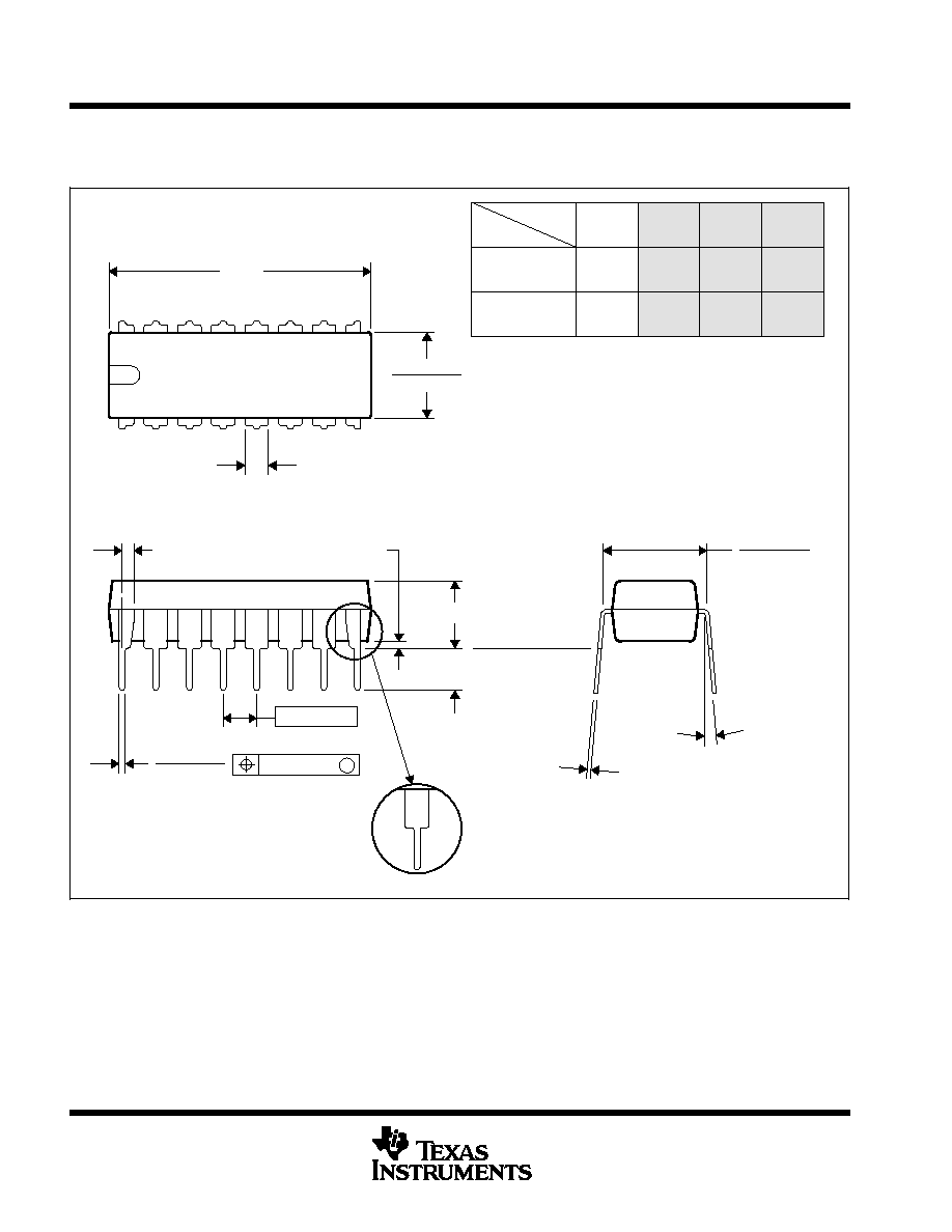
TLE206x, TLE206xA, TLE206xB, TLE206xY
EXCALIBUR JFET-INPUT HIGH-OUTPUT-DRIVE
µ
POWER OPERATIONAL AMPLIFIERS
SLOS193A ≠ FEBRUARY 1997 ≠ REVISED MARCH 1998
66
POST OFFICE BOX 655303
∑
DALLAS, TEXAS 75265
MECHANICAL INFORMATION
N (R-PDIP-T**)
PLASTIC DUAL-IN-LINE PACKAGE
20
0.975
(24,77)
0.940
(23,88)
18
0.920
0.850
14
0.775
0.745
(19,69)
(18,92)
16
0.775
(19,69)
(18,92)
0.745
A MIN
DIM
A MAX
PINS **
0.310 (7,87)
0.290 (7,37)
(23.37)
(21.59)
Seating Plane
0.010 (0,25) NOM
14/18 PIN ONLY
4040049/C 08/95
9
8
0.070 (1,78) MAX
A
0.035 (0,89) MAX
0.020 (0,51) MIN
16
1
0.015 (0,38)
0.021 (0,53)
0.200 (5,08) MAX
0.125 (3,18) MIN
0.240 (6,10)
0.260 (6,60)
M
0.010 (0,25)
0.100 (2,54)
0
∞
≠ 15
∞
16 PIN SHOWN
NOTES: A. All linear dimensions are in inches (millimeters).
B. This drawing is subject to change without notice.
C. Falls within JEDEC MS-001 (20 pin package is shorter then MS-001.)
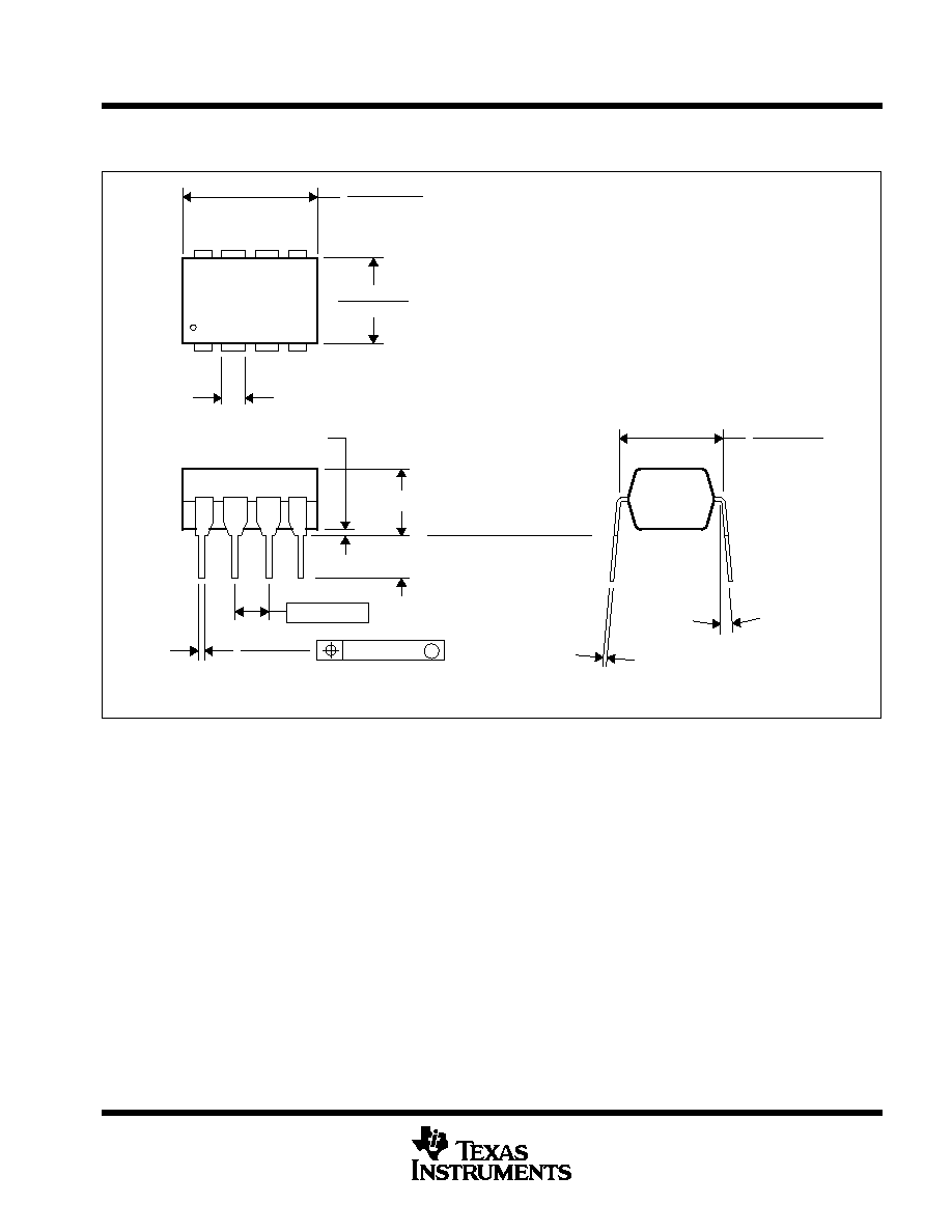
TLE206x, TLE206xA, TLE206xB, TLE206xY
EXCALIBUR JFET-INPUT HIGH-OUTPUT-DRIVE
µ
POWER OPERATIONAL AMPLIFIERS
SLOS193A ≠ FEBRUARY 1997 ≠ REVISED MARCH 1998
67
POST OFFICE BOX 655303
∑
DALLAS, TEXAS 75265
MECHANICAL INFORMATION
P (R-PDIP-T8)
PLASTIC DUAL-IN-LINE PACKAGE
4040082 / B 03/95
0.310 (7,87)
0.290 (7,37)
0.010 (0,25) NOM
0.400 (10,60)
0.355 (9,02)
5
8
4
1
0.020 (0,51) MIN
0.070 (1,78) MAX
0.240 (6,10)
0.260 (6,60)
0.200 (5,08) MAX
0.125 (3,18) MIN
0.015 (0,38)
0.021 (0,53)
Seating Plane
M
0.010 (0,25)
0.100 (2,54)
0
∞
≠ 15
∞
NOTES: A. All linear dimensions are in inches (millimeters).
B. This drawing is subject to change without notice.
C. Falls within JEDEC MS-001
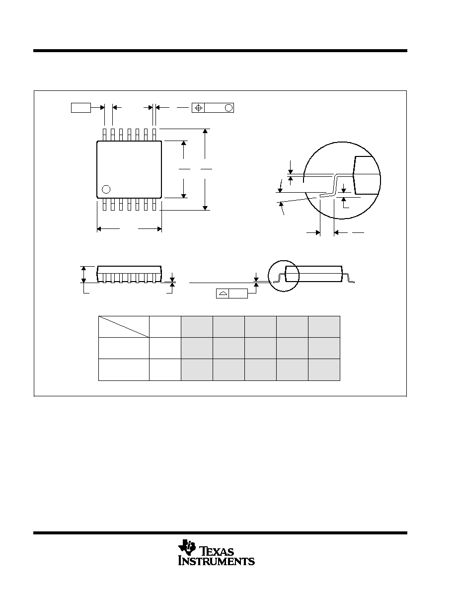
TLE206x, TLE206xA, TLE206xB, TLE206xY
EXCALIBUR JFET-INPUT HIGH-OUTPUT-DRIVE
µ
POWER OPERATIONAL AMPLIFIERS
SLOS193A ≠ FEBRUARY 1997 ≠ REVISED MARCH 1998
68
POST OFFICE BOX 655303
∑
DALLAS, TEXAS 75265
MECHANICAL INFORMATION
PW (R-PDSO-G**)
PLASTIC SMALL-OUTLINE PACKAGE
4040064 / E 08/96
14 PIN SHOWN
Seating Plane
0,05 MIN
1,20 MAX
1
A
7
14
0,19
4,50
4,30
8
6,20
6,60
0,30
0,75
0,50
0,25
Gage Plane
0,15 NOM
0,65
M
0,10
0
∞
≠ 8
∞
0,10
PINS **
A MIN
A MAX
DIM
2,90
3,10
8
4,90
5,10
14
6,60
6,40
4,90
5,10
16
7,70
20
7,90
24
9,60
9,80
28
NOTES: A. All linear dimensions are in millimeters.
B. This drawing is subject to change without notice.
C. Body dimensions do not include mold flash or protrusion not to exceed 0,15.
D. Falls within JEDEC MO-153

IMPORTANT NOTICE
Texas Instruments and its subsidiaries (TI) reserve the right to make changes to their products or to discontinue
any product or service without notice, and advise customers to obtain the latest version of relevant information
to verify, before placing orders, that information being relied on is current and complete. All products are sold
subject to the terms and conditions of sale supplied at the time of order acknowledgement, including those
pertaining to warranty, patent infringement, and limitation of liability.
TI warrants performance of its semiconductor products to the specifications applicable at the time of sale in
accordance with TI's standard warranty. Testing and other quality control techniques are utilized to the extent
TI deems necessary to support this warranty. Specific testing of all parameters of each device is not necessarily
performed, except those mandated by government requirements.
CERTAIN APPLICATIONS USING SEMICONDUCTOR PRODUCTS MAY INVOLVE POTENTIAL RISKS OF
DEATH, PERSONAL INJURY, OR SEVERE PROPERTY OR ENVIRONMENTAL DAMAGE ("CRITICAL
APPLICATIONS"). TI SEMICONDUCTOR PRODUCTS ARE NOT DESIGNED, AUTHORIZED, OR
WARRANTED TO BE SUITABLE FOR USE IN LIFE-SUPPORT DEVICES OR SYSTEMS OR OTHER
CRITICAL APPLICATIONS. INCLUSION OF TI PRODUCTS IN SUCH APPLICATIONS IS UNDERSTOOD TO
BE FULLY AT THE CUSTOMER'S RISK.
In order to minimize risks associated with the customer's applications, adequate design and operating
safeguards must be provided by the customer to minimize inherent or procedural hazards.
TI assumes no liability for applications assistance or customer product design. TI does not warrant or represent
that any license, either express or implied, is granted under any patent right, copyright, mask work right, or other
intellectual property right of TI covering or relating to any combination, machine, or process in which such
semiconductor products or services might be or are used. TI's publication of information regarding any third
party's products or services does not constitute TI's approval, warranty or endorsement thereof.
Copyright
©
1998, Texas Instruments Incorporated