TLE2161, TLE2161A, TLE2161B
EXCALIBUR JFET-INPUT HIGH-OUTPUT-DRIVE
µ
POWER OPERATIONAL AMPLIFIERS
SLOS049D ≠ NOVEMBER 1989 ≠ REVISED MAY 1996
1
POST OFFICE BOX 655303
∑
DALLAS, TEXAS 75265
D
Excellent Output Drive Capability
V
O
=
±
2.5 V Min at R
L
= 100
,
V
CC
±
=
±
5 V
V
O
=
±
12.5 V Min at R
L
= 600
,
V
CC
±
=
±
15 V
D
Low Supply Current . . . 280
µ
A Typ
D
Decompensated for High Slew Rate and
Gain-Bandwidth Product
A
VD
= 0.5 Min
Slew Rate = 10 V/
µ
s Typ
Gain-Bandwidth Product = 6.5 MHz Typ
D
Wide Operating Supply Voltage Range
V
CC
±
=
±
3.5 V to
±
18 V
D
High Open-Loop Gain . . . 280 V/mV Typ
D
Low Offset Voltage . . . 500
µ
V Max
D
Low Offset Voltage Drift With Time
0.04
µ
V/Month Typ
D
Low Input Bias Current . . . 5 pA Typ
description
The TLE2161, TLE2161A, and TLE2161B are
JFET-input, low-power, precision operational
amplifiers manufactured using the Texas
Instruments Excalibur process. Decompensated
for stability with a minimum closed-loop gain of 5,
these devices combine outstanding output drive
capability with low power consumption, excellent
dc precision, and high gain-bandwidth product.
In addition to maintaining the traditional JFET
advantages of fast slew rates and low input bias
and offset currents, the Excalibur process offers
outstanding parametric stability over time and
temperature. This results in a device that remains
precise even with changes in temperature and
over years of use.
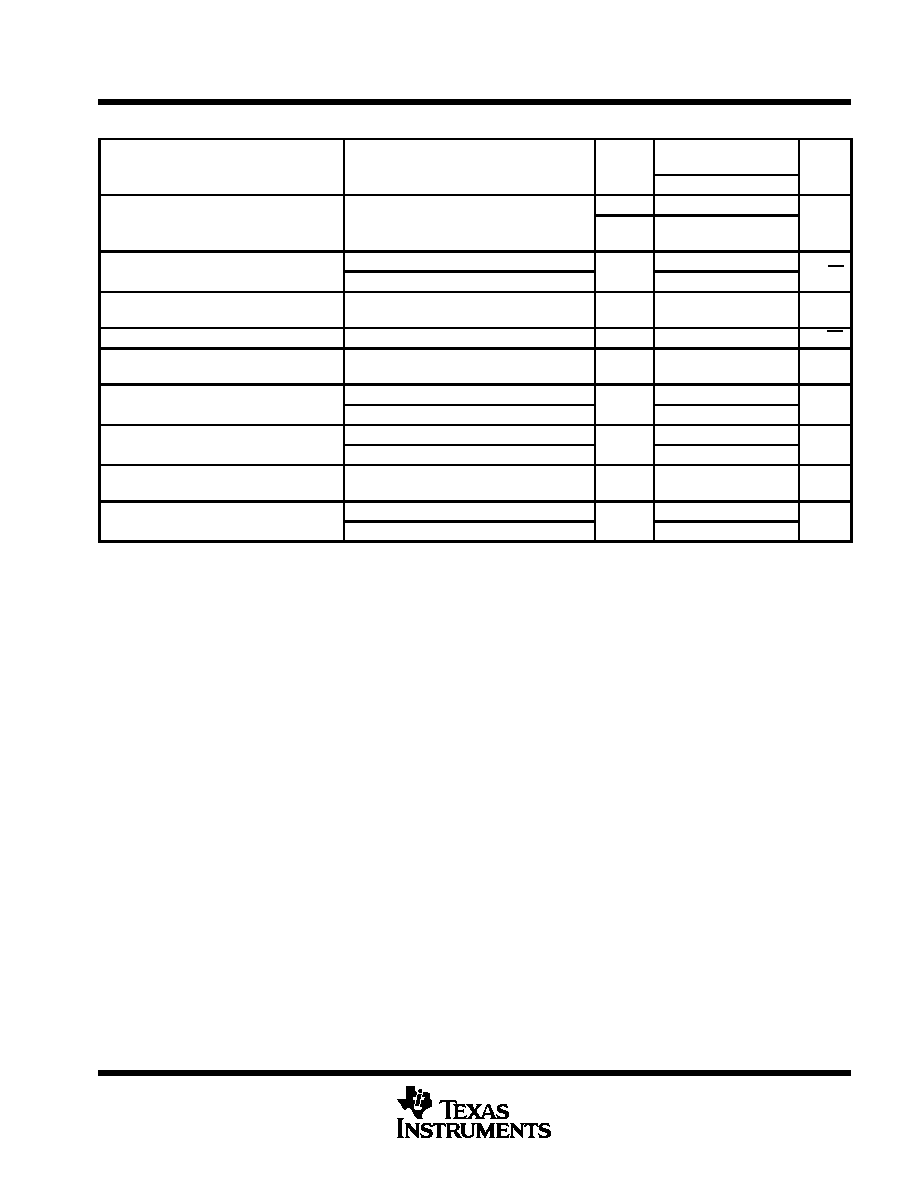
AVAILABLE OPTIONS
PACKAGE
TA
VIOmax
AT 25
∞
C
SMALL
OUTLINE
CHIP
CARRIER
CERAMIC
DIP
PLASTIC
DIP
AT 25 C
OUTLINE
(D)
CARRIER
(FK)
DIP
(JG)
DIP
(P)
0
∞
C
to
500
µ
V
1 5 mV
--
TLE2161ACD
--
--
TLE2161BCP
TLE2161ACP
to
70
∞
C
1.5 mV
3 mV
TLE2161ACD
TLE2161CD
--
--
TLE2161ACP
TLE2161CP
≠ 40
∞
C
to
500
µ
V
1 5 mV
--
TLE2161AID
--
--
TLE2161BIP
TLE2161AIP
to
85
∞
C
1.5 mV
3 mV
TLE2161AID
TLE2161ID
--
--
TLE2161AIP
TLE2161IP
≠ 55
∞
C
to
500
µ
V
1 5 mV
--
TLE2161AMD
--
TLE2161AMFK
TLE2161BMJG
TLE2161AMJG
TLE2161BMP
TLE2161AMP
to
125
∞
C
1.5 mV
3 mV
TLE2161AMD
TLE2161MD
TLE2161AMFK
TLE2161MFK
TLE2161AMJG
TLE2161MJG
TLE2161AMP
TLE2161MP
The D packages are available taped and reeled. Add R suffix to device type (e.g., TLE2161ACDR).
Please be aware that an important notice concerning availability, standard warranty, and use in critical applications of
Texas Instruments semiconductor products and disclaimers thereto appears at the end of this data sheet.
PRODUCTION DATA information is current as of publication date.
Products conform to specifications per the terms of Texas Instruments
standard warranty. Production processing does not necessarily include
testing of all parameters.
Copyright
©
1996, Texas Instruments Incorporated
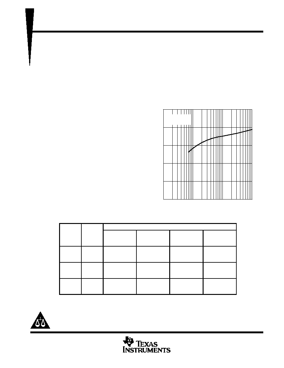
10 k
1 k
100
RL ≠ Load Resistance ≠
10
0
2
4
6
8
10
TA = 25
∞
C
MAXIMUM PEAK-TO-PEAK OUTPUT VOLTAGE
vs
LOAD RESISTANCE
≠ Maximum Peak-to-Peak Output V
oltage ≠ V
V
O(PP)
VCC
±
=
±
5 V
TLE2161, TLE2161A, TLE2161B
EXCALIBUR JFET-INPUT HIGH-OUTPUT-DRIVE
µ
POWER OPERATIONAL AMPLIFIERS
SLOS049D ≠ NOVEMBER 1989 ≠ REVISED MAY 1996
2
POST OFFICE BOX 655303
∑
DALLAS, TEXAS 75265
description (continued)
A variety of available options includes small-outline packages and chip-carrier versions for high-density system
applications.
The C-suffix devices are characterized for operation from 0
∞
C to 70
∞
C. The I-suffix devices are characterized
for operation from ≠ 40
∞
C to 85
∞
C. The M-suffix devices are characterized for operation over the full military
temperature range of ≠ 55
∞
C to 125
∞
C.
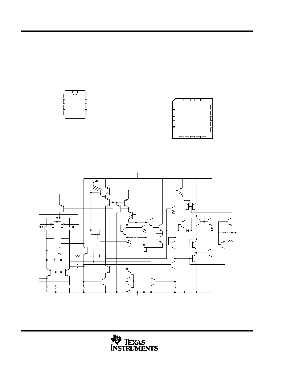
NC
1
2
3
4
8
7
6
5
OFFSET N1
IN ≠
IN +
V
CC ≠
NC
V
CC +
OUT
OFFSET N2
D, JG, OR P PACKAGE
(TOP VIEW)
NC ≠ No internal connection
3
2
1 20 19
9 10 11 12 13
4
5
6
7
8
18
17
16
15
14
NC
V
CC +
NC
OUT
NC
NC
IN ≠
NC
IN +
NC
FK PACKAGE
(TOP VIEW)
NC
N1
NC
NC
NC
NC
NC
N2
CC
≠
V
equivalent schematic
Q35
Q34
2.7 k
Q10
Q15
VCC ≠
Q2
OFFSET N2
OFFSET N1
1.1 k
R1
15 pF
C1
55 k
1.1 k
R4
R2
Q8
C2 15 pF
Q6
2.4 k
R3
60 k
R5
Q12
Q22
Q21
Q26
Q7
IN ≠
IN +
1.6 pF
C3
Q11
Q20
Q24
Q16
Q17
Q23
R6
Q19
Q18
Q25
Q27
Q28
600
R7
Q31
Q30
Q38
Q39
Q41
Q42
OUT
100
R9
20
R8
Q29
Q43
Q40
Q37
Q36
Q33
Q32
Q5
Q1
Q3
Q14
Q13
Q9
Q4
VCC +
All component values are nominal.
TLE2161, TLE2161A, TLE2161B
EXCALIBUR JFET-INPUT HIGH-OUTPUT-DRIVE
µ
POWER OPERATIONAL AMPLIFIERS
SLOS049D ≠ NOVEMBER 1989 ≠ REVISED MAY 1996
3
POST OFFICE BOX 655303
∑
DALLAS, TEXAS 75265
absolute maximum ratings over operating free-air temperature range (unless otherwise noted)
Supply voltage, V
CC +
(see Note 1)
19 V
. . . . . . . . . . . . . . . . . . . . . . . . . . . . . . . . . . . . . . . . . . . . . . . . . . . . . . . . . .
Supply voltage, V
CC ≠
≠ 19 V
. . . . . . . . . . . . . . . . . . . . . . . . . . . . . . . . . . . . . . . . . . . . . . . . . . . . . . . . . . . . . . . . . . . .
Differential input voltage, V
ID
(see Note 2)
±
38 V
. . . . . . . . . . . . . . . . . . . . . . . . . . . . . . . . . . . . . . . . . . . . . . . . . .
Input voltage range, V
I
(any input)
V
CC
±
. . . . . . . . . . . . . . . . . . . . . . . . . . . . . . . . . . . . . . . . . . . . . . . . . . . . . . . . . . .
Input current, I
I
(each input)
±
1 mA
. . . . . . . . . . . . . . . . . . . . . . . . . . . . . . . . . . . . . . . . . . . . . . . . . . . . . . . . . . . . . . .
Output current, I
O
±
80 mA
. . . . . . . . . . . . . . . . . . . . . . . . . . . . . . . . . . . . . . . . . . . . . . . . . . . . . . . . . . . . . . . . . . . . . . .
Total current into V
CC +
80 mA
. . . . . . . . . . . . . . . . . . . . . . . . . . . . . . . . . . . . . . . . . . . . . . . . . . . . . . . . . . . . . . . . . . .
Total current out of V
CC ≠
80 mA
. . . . . . . . . . . . . . . . . . . . . . . . . . . . . . . . . . . . . . . . . . . . . . . . . . . . . . . . . . . . . . . . .
Duration of short-circuit current at (or below) 25
∞
C (see Note 3)
unlimited
. . . . . . . . . . . . . . . . . . . . . . . . . . . . . .
Continuous total power dissipation
See Dissipation Rating Table
. . . . . . . . . . . . . . . . . . . . . . . . . . . . . . . . . . . . .
Operating free-air temperature range, T
A
: C suffix
0
∞
C to 70
∞
C
. . . . . . . . . . . . . . . . . . . . . . . . . . . . . . . . . . . . . .
I suffix
≠ 40
∞
C to 85
∞
C
. . . . . . . . . . . . . . . . . . . . . . . . . . . . . . . . . . . . .
M suffix
≠ 55
∞
C to 125
∞
C
. . . . . . . . . . . . . . . . . . . . . . . . . . . . . . . . .
Storage temperature range, T
stg
≠ 65
∞
C to 150
∞
C
. . . . . . . . . . . . . . . . . . . . . . . . . . . . . . . . . . . . . . . . . . . . . . . . . .
Case temperature for 60 seconds: FK package
260
∞
C
. . . . . . . . . . . . . . . . . . . . . . . . . . . . . . . . . . . . . . . . . . . . . .
Lead temperature 1,6 mm (1/16 inch) from case for 10 seconds: D or P package
260
∞
C
. . . . . . . . . . . . . . . . .
Lead temperature 1,6 mm (1/16 inch) from case for 60seconds: JG package
300
∞
C
. . . . . . . . . . . . . . . . . . . .
Stresses beyond those listed under "absolute maximum ratings" may cause permanent damage to the device. These are stress ratings only, and
functional operation of the device at these or any other conditions beyond those indicated under "recommended operating conditions" is not
implied. Exposure to absolute-maximum-rated conditions for extended periods may affect device reliability.
NOTES:
1. All voltage values, except differential voltages, are with respect to the midpoint between VCC +, and VCC ≠.
2. Differential voltages are at IN+ with respect to IN ≠.
3. The output may be shorted to either supply. Temperature and /or supply voltages must be limited to ensure that the maximum
dissipation rating is not exceeded.
DISSIPATION RATING TABLE
PACKAGE
TA
25
∞
C
POWER RATING
DERATING FACTOR
ABOVE TA = 25
∞
C
TA = 70
∞
C
POWER RATING
TA = 85
∞
C
POWER RATING
TA = 125
∞
C
POWER RATING
D
725 mW
5.8 mW/
∞
C
464 mW
377 mW
145 mW
FK
1375 mW
11.0 mW/
∞
C
880 mW
715 mW
275 mW
JG
1050 mW
8.4 mW/
∞
C
672 mW
546 mW
210 mW
P
1000 mW
8.0 mW/
∞
C
640 mW
520 mW
200 mW
recommended operating conditions
C SUFFIX
I SUFFIX
M SUFFIX
UNIT
MIN
MAX
MIN
MAX
MIN
MAX
UNIT
Supply voltage, VCC
±
±
3.5
±
18
±
3.5
±
18
+
3.5
±
18
V
Common mode input voltage VIC
VCC
±
=
±
5 V
≠ 1.6
4
≠ 1.6
4
≠ 1.6
4
V
Common-mode input voltage, VIC
VCC
±
=
±
15 V
≠ 11
13
≠ 11
13
≠ 11
13
V
Operating free-air temperature, TA
0
70
≠ 40
85
≠ 55
125
∞
C
TLE2161, TLE2161A, TLE2161B
EXCALIBUR JFET-INPUT HIGH-OUTPUT-DRIVE
µ
POWER OPERATIONAL AMPLIFIERS
SLOS049D ≠ NOVEMBER 1989 ≠ REVISED MAY 1996
4
POST OFFICE BOX 655303
∑
DALLAS, TEXAS 75265
electrical characteristics at specified free-air temperature, V
CC
±
=
±
5 V (unless otherwise noted)
PARAMETER
TEST CONDITIONS
TA
TLE2161C, TLE2161AC
TLE2161BC
UNIT
A
MIN
TYP
MAX
TLE2161C
25
∞
C
0.8
3.1
TLE2161C
Full range
4
VIO
Input offset voltage
TLE2161AC
25
∞
C
0.6
2.6
mV
VIO
Input offset voltage
TLE2161AC
Full range
3.5
mV
TLE2161BC
25
∞
C
0.5
1.9
TLE2161BC
VIC = 0
RS = 50
Full range
2.4
VIO
Temperature coefficient of input offset voltage
VIC = 0,
RS = 50
Full range
6
µ
V/
∞
C
Input offset voltage long-term drift (see Note 4)
25
∞
C
0.04
µ
V/mo
IIO
Input offset current
25
∞
C
1
pA
IIO
Input offset current
Full range
0.8
nA
IIB
Input bias current
25
∞
C
3
pA
IIB
Input bias current
Full range
2
nA
VICR
Common mode input voltage range
25
∞
C
≠ 1.6
to 4
≠ 2
to 6
V
VICR
Common-mode input voltage range
Full range
≠ 1.6
to 4
V
RL = 10
k
25
∞
C
3.5
3.7
VOM
Maximum positive peak output voltage swing
RL = 10
k
Full range
3.3
V
VOM + Maximum positive peak output voltage swing
RL = 100
25
∞
C
2.5
3.1
V
RL = 100
Full range
2
RL = 10
k
25
∞
C
≠ 3.7
≠ 3.9
VOM
Maximum negative peak output voltage swing
RL = 10
k
Full range
≠ 3.3
V
VOM ≠ Maximum negative peak output voltage swing
RL = 100
25
∞
C
≠ 2.5
≠ 2.7
V
RL = 100
Full range
≠ 2
VO =
±
2 8 V
RL = 10 k
25
∞
C
15
80
VO =
±
2.8 V,
RL = 10 k
Full range
2
AVD
Large signal differential voltage amplification
VO = 0 to 2 V
RL = 100
25
∞
C
0.75
45
V/mV
AVD
Large-signal differential voltage amplification
VO = 0 to 2 V, RL = 100
Full range
0.5
V/mV
VO = 0 to 2 V
RL = 100
25
∞
C
0.5
3
VO = 0 to ≠ 2 V, RL = 100
Full range
0.25
ri
Input resistance
25
∞
C
1012
ci
Input capacitance
25
∞
C
4
pF
zo
Open-loop output impedance
IO = 0
25
∞
C
280
CMRR
Common mode rejection ratio
VIC=VICRmin
RS = 50
25
∞
C
65
82
dB
CMRR
Common-mode rejection ratio
VIC = VICRmin, RS = 50
Full range
65
dB
kSVR
Supply voltage rejection ratio (
VCC
±
/
VIO)
VCC
±
=
±
5 V to
±
15 V,
25
∞
C
75
93
dB
kSVR
Supply-voltage rejection ratio (
VCC
±
/
VIO)
VCC
±
±
5 V to
±
15 V,
RS = 50
Full range
75
dB
ICC
Supply current
25
∞
C
280
325
µ
A
ICC
Supply current
VO = 0
No load
Full range
350
µ
A
ICC
Supply-current change over operating
VO = 0,
No load
Full range
29
µ
A
ICC
y
g
g
temperature range
Full range
29
µ
A
Full range is 0
∞
C to 70
∞
C.
NOTE 4: Typical values are based on the input offset voltage shift observed through 168 hours of operating life test at TA = 150
∞
C extrapolated
to TA = 25
∞
C using the Arrhenius equation and assuming an activation energy of 0.96 eV.
TLE2161, TLE2161A, TLE2161B
EXCALIBUR JFET-INPUT HIGH-OUTPUT-DRIVE
µ
POWER OPERATIONAL AMPLIFIERS
SLOS049D ≠ NOVEMBER 1989 ≠ REVISED MAY 1996
5
POST OFFICE BOX 655303
∑
DALLAS, TEXAS 75265
operating characteristics at specified free-air temperature, V
CC
±
=
±
5 V (unless otherwise noted)
PARAMETER
TEST CONDITIONS
TA
TLE2161C, TLE2161AC
TLE2161BC
UNIT
A
MIN
TYP
MAX
25
∞
C
7
10
SR
Slew rate (see Figure 1)
AVD = 5,
RL = 10 k
,
CL = 100 pF
Full
range
5
V/
µ
s
V
Equivalent input noise voltage
RS = 20
,
f = 10 Hz
25
∞
C
59
100
nV/
H
Vn
q
g
(see Figure 2)
RS = 20
,
f = 1 kHz
25
∞
C
43
60
nV/
Hz
Vn(PP)
Peak-to-peak equivalent input
noise voltage
f = 0.1 Hz to 10 Hz
25
∞
C
1.1
µ
V
In
Equivalent input noise current
f = 1 kHz
25
∞
C
1
fA/
Hz
THD
Total harmonic distortion
VO(PP) = 2 V,
RL = 10 k
AVD
= 5,
f = 10 kHz,
25
∞
C
0.025%
Gain-bandwidth product
f = 100 kHz,
RL = 10 k
,
CL = 100 pF
25
∞
C
5.8
MHz
(see Figure 3)
f = 100 kHz,
RL
= 100 k
,
CL = 100 pF
25
∞
C
4.3
MHz
t
Settling time
= 0.1%
25
∞
C
5
µ
s
ts
Settling time
= 0.01%
25
∞
C
10
µ
s
BOM
Maximum output-swing
bandwidth
AVD = 5,
RL
= 10 k
25
∞
C
420
kHz
Phase margin (see Figure 3)
AVD = 5,
RL
= 10 k
,
CL = 100 pF
25
∞
C
70
∞
m
Phase margin (see Figure 3)
AVD = 5,
RL
= 100
,
CL = 100 pF
25
∞
C
84
∞
Full range is 0
∞
C to 70
∞
C.