
TLV320AIC28
SLAS418A - FEBRUARY 2004 - REVISED SEPTEMBER 2004
STEREO AUDIO CODEC WITH INTEGRATED HEADPHONE AND
SPEAKER AMPLIFIERS
FEATURES
D
Stereo Audio DAC and Mono Audio ADC
Support Rates Up to 48 ksps
D
High Quality 95-dB Stereo Audio Playback
Performance
D
MIC Preamp and Hardware Automatic Gain
Control With Up to 59.5-dB Gain
D
Stereo 16-
W
Headphone Amplifier With
Capless Output Option
D
400-mW 8-
W
Audio Power Amp With Direct
Battery Supply Connection
D
32-
W
Differential Earpiece Driver
D
Integrated PLL For Flexible Audio Clock
Generation
D
Low Power 19-mW Stereo Audio Playback at
48 ksps and 3.3-V Analog Supply level
D
Programmable Digital Audio Bass/Treble/
EQ/De-Emphasis
D
Auto-Detection of Jack Insertion, Headset
Type, and Button Press
D
Direct Battery Measurement Accepts Up to
6-V Input
D
On-Chip Temperature and Auxiliary Input
Measurement
D
Programmable Measurement Converter
Resolution, Speed, Averaging, and Timing
D
SPI
and I
2
S
Serial Interfaces
D
Full Power-Down Control
D
48-Pin QFN Package
APPLICATIONS
D
Personal Digital Assistants
D
Cellular Smartphones
D
Digital Still Cameras
D
Digital Camcorders
D
MP3 Players
DESCRIPTION
The TLV320AIC28 is a low-power, high-performance
audio codec with 16/20/24/32-bit 95-dB stereo playback,
mono record functionality at up to 48 ksps. Two
microphone inputs include independent programmable
bias voltages, built-in pre-amps, and hardware automatic
gain control, with single-ended or fully-differential signal
input capabilities.
The stereo 16-
headphone drivers on the AIC28 support
capless as well as ac-coupled output configurations. An
8-
BTL differential speaker driver provides up to 400 mW
of power and 98-dB SNR, while a differential driver is also
available for driving a 32-
speaker or telephone earpiece.
A programmable digital audio effects processor enables
bass, treble, midrange, or equalization playback
processing. The digital audio data format is programmable
to work with popular audio standard protocols (I
2
S, DSP,
left/right justified) in master or slave mode, and also
includes an on-chip programmable PLL for flexible clock
generation capability. Highly configurable software power
control is provided, enabling 48 ksps stereo audio
playback to 16-
headphones at 19 mW with a 3.3-V
analog supply level.
The AIC28 offers a 12-bit measurement ADC and internal
reference voltage. It includes an on-chip temperature
sensor capable of reading 0.3
∞
C resolution, as well as a
battery measurement input capable of reading battery
voltages up to 6 V, while operating at an analog supply as
low as 3 V. The AIC28 is available in a 48-lead 7 x 7 mm
QFN package.
US Patent No. 624639
SPI is a trademark of Motorola, Inc. I2S is a trademark of Philips Corporation.
PRODUCTION DATA information is current as of publication date. Products
conform to specifications per the terms of Texas Instruments standard warranty.
Production processing does not necessarily include testing of all parameters.
Please be aware that an important notice concerning availability, standard warranty, and use in critical applications of Texas Instruments
semiconductor products and disclaimers thereto appears at the end of this data sheet.
www.ti.com
Copyright
2004, Texas Instruments Incorporated

TLV320AIC28
SLAS418A - FEBRUARY 2004 - REVISED SEPTEMBER 2004
www.ti.com
2
This integrated circuit can be damaged by ESD. Texas Instruments recommends that all integrated circuits be handled with appropriate
precautions. Failure to observe proper handling and installation procedures can cause damage.
ESD damage can range from subtle performance degradation to complete device failure. Precision integrated circuits may be more susceptible to
damage because very small parametric changes could cause the device not to meet its published specifications.
PACKAGE/ORDERING INFORMATION
PRODUCT
PACKAGE
PACKAGE
DESIGNATOR
OPERATING
TEMPERATURE RANGE
ORDERING NUMBER
TRANSPORT MEDIA
TLV320AIC28
QFN-48
RGZ
-40
∞
C to +85
∞
C
TLV320AIC28IRGZ
Rails, 52
TLV320AIC28
QFN-48
RGZ
-40
∞
C to +85
∞
C
TLV320AIC28IRGZR
Tape and Reel, 2500
PIN ASSIGNMENTS
QFN PACKAGE
(TOP VIEW)
13
DRVSS2
OUT8P
BVDD
OUT8N
DRVSS1
VGND
SPKFC
DRVDD
SPK2
SPK1
OUT32N
MIC_DETECT_IN
36
35
34
33
32
31
30
29
28
27
26
25
1
2
3
4
5
6
7
8
9
10
11
12
IOVDD
PWR_DN
RESET
GPIO2
GPIO1
AVDD2
AVSS2
AVDD1
NC
NC
NC
NC
14 15 16 17 18 19 20 21 22 23 24
48 47 46 45 44 43 42 41 40 39 38 37
A
VSS1
VREF
VBA
T
AUX2
AUX1
BUZZ_IN
CP_OUT
CP_IN
MICIN_HND
MICBIAS_HND
MICIN_HED
MICBIAS_HED
DVSS
DVDD
BCLK
WCLK
SDIN
SDOUT
MCLK
SCLK
MISO
MOSI
SS
DA
V

TLV320AIC28
SLAS418A - FEBRUARY 2004 - REVISED SEPTEMBER 2004
www.ti.com
3
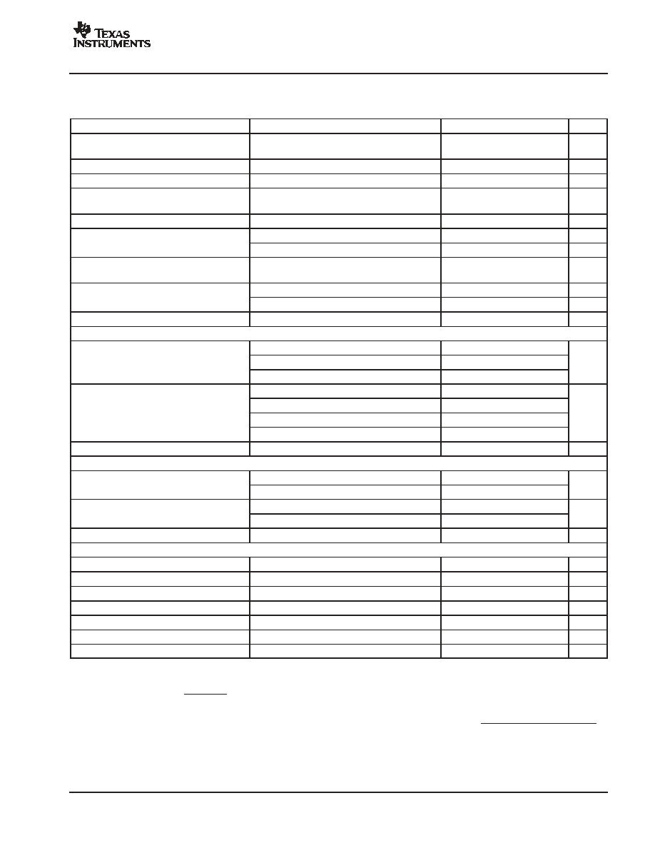
Terminal Functions
PIN
NAME
DESCRIPTION
PIN
NAME
DESCRIPTION
1
IOVDD
IO Supply
25
MIC_DETECT_IN
Microphone detect input
2
PWR_DN
Hardware power down
26
OUT32N
Receiver driver output
3
RESET
Hardware reset
27
SPK1
Headset driver output/receiver driver output
4
GPIO2
General purpose IO
28
SPK2
Headset driver output
5
GPIO1
General purpose IO
29
DRVDD
Headphone driver power supply
6
AVDD2
PLL analog power supply
30
SPKFC
Driver feedback/ speaker detect input
7
AVSS2
Analog ground
31
VGND
Virtual ground for audio output
8
AVDD1
Audio ADC, DAC, reference, SAR
ADC analog power supply
32
DRVSS1
Driver ground
9
NC
No connect
33
OUT8N
Loudspeaker driver output
10
NC
No connect
34
BVDD
Battery power supply
11
NC
No connect
35
OUT8P
Loudspeaker driver output
12
NC
No connect
36
DRVSS2
Driver ground
13
AVSS1
Analog ground
37
DAV
Auxiliary data available output
14
VREF
Reference voltage for SAR ADC
38
SS
SPI Slave select input
15
VBAT
Battery monitor input
39
MOSI
SPI Serial data input
16
AUX2
Secondary auxiliary input
40
MISO
SPI Serial data output
17
AUX1
First auxiliary input
41
SCLK
SPI Serial clock input
18
BUZZ_IN
Buzzer input
42
MCLK
Master clock
19
CP_OUT
Output to cell phone module
43
SDOUT
Audio data output
20
CP_IN
Input from cell phone module
44
SDIN
Audio data input
21
MICIN_HND
Handset microphone input
45
WCLK
Audio word clock
22
MICBIAS_HND
Handset microphone bias voltage
46
BCLK
Audio bit clock
23
MICIN_HED
Headset microphone input
47
DVDD
Digital core supply
24
MICBIAS_HED
Headset microphone bias voltage
48
DVSS
Digital core and IO ground
ABSOLUTE MAXIMUM RATINGS
over operating free-air temperature range unless otherwise noted(1), (2)
UNITS
AVDD1/2 to AVSS1/2
-0.3 V to 3.9 V
DRVDD to DRVSS1/2
-0.3 V to 3.9 V
BVDD to DRVSS1/2
-0.3 V to 4.5 V
IOVDD to DVSS
-0.3 V to 3.9 V
Digital input voltage to DVSS
-0.3 V to IOVDD + 0.3 V
Analog input (except VBAT) voltage to AVSS1/2
-0.3 V to AVDD + 0.3 V
VBAT input voltage to AVSS1/2
-0.3 V to 6 V
AVSS1/2 to DRVSS1/2 to DVSS
-0.1 V to 0.1 V
AVDD1/2 to DRVDD
-0.1 V to 0.1 V
Operating temperature range
-40
∞
C to 85
∞
C
Storage temperature range
-65
∞
C to 105
∞
C
Junction temperature (TJ Max)
105
∞
C
QFN package
Power dissipation
(TJ Max - TA)/
JA
QFN package
JA Thermal impedance (with thermal pad soldered to board)
27
∞
C/W
Lead temperature
Infrared (15 sec)
240
∞
C
(1) Stresses beyond those listed under "absolute maximum ratings" may cause permanent damage to the device. These are stress ratings only, and
functional operation of the device at these or any other conditions beyond those indicated under "recommended operating conditions" is not
implied. Exposure to absolute-maximum-rated conditions for extended periods may affect device reliability.
(2) If the AIC28 is used to drive high power levels to an 8-
load for extended intervals at an ambient temperature above 80
∞
C, multiple vias should
be used to electrically and thermally connect the thermal pad on the QFN package to an internal heat dissipating ground plane on the user's PCB.

TLV320AIC28
SLAS418A - FEBRUARY 2004 - REVISED SEPTEMBER 2004
www.ti.com
4
ELECTRICAL CHARACTERISTICS
At +25
∞
C, AVDD1, AVDD2, DRVDD, IOVDD = 3.3 V, BVDD = 3.9 V, DVDD = 1.8 V, Vref = 2.5 V, Fs (Audio) = 48 kHz, unless otherwise noted
PARAMETER
TEST CONDITIONS
MIN
TYP
MAX
UNITS
BATTERY MONITOR INPUTS
Input voltage range
0.5
6.0
V
Input leakage current
Battery conversion not selected
±
1
µ
A
Accuracy
Variation across temperature after system
calibration at 4 V battery voltage and room
temperature
±
15
mV
AUXILIARY A/D CONVERTER
Resolution
Programmable: 8-, 10-,12-bits
8
12
Bits
No missing codes
12-Bit resolution
11
Bits
Integral nonlinearity
-5
5
LSB
Offset error
-6
6
LSB
Gain error
-6
6
LSB
Noise
50
µ
Vrms
VOLTAGE REFERENCE (VREF)
VREF output programmed = 2.5 V
2.3
2.5
2.7
V
Voltage range
VREF output programmed = 1.25 V
1.25
V
Voltage range
External reference
1.1
2.5
V
Reference drift
Internal VREF = 1.25 V
50
ppm/
∞
C
Current drain
Extra current drawn when the internal reference is
turned on.
750
µ
A
AUDIO CODEC
ADC DECIMATION FILTER CHARACTERISTICS
Filter gain from 0 to 0.39 Fs
±
0.1
dB
Filter gain at 0.4125 Fs
-0.25
dB
Filter gain at 0.45 Fs
-3.0
dB
Filter gain at 0.5 Fs
-17.5
dB
Filter gain from 0.55 Fs to 64 Fs
-75
dB
Group delay
17/Fs
sec
TLV320AIC28
SLAS418A - FEBRUARY 2004 - REVISED SEPTEMBER 2004
www.ti.com
5
ELECTRICAL CHARACTERISTICS (continued)
At +25
∞
C, AVDD1, AVDD2, DRVDD, IOVDD = 3.3 V, BVDD = 3.9 V, DVDD = 1.8 V, Int. Vref = 2.5 V, Fs (Audio) = 48 kHz, unless otherwise
noted (continued)
PARAMETER
TEST CONDITIONS
MIN
TYP
MAX
UNITS
MICROPHONE INPUT TO ADC
MICIN_HED 1020 Hz sine wave input,
Fs = 48 ksps
Full-scale input voltage (0 dB)
0.707
Vrms
Input common mode
1.5
V
SNR
Measured as idle channel noise, 0 dB gain,
A-weighted
80
90
dBA
THD
0.63 Vrms input, 0-dB gain
-81
-72
dB
PSRR
217 Hz, 100 mV on AVDD1/2(1)
55
dB
PSRR
1020 Hz, 100 mV on AVDD1/2(1)
55
dB
Mute attenuation
Output code with 0.63 Vrms sine wave input at
1 kHz
0000H
Input resistance
Only ADC on
15
50
k
Input resistance
ADC and Sidetone on
8
16
k
Input capacitance
10
pF
HEADSET MICROPHONE BIAS
Register 1DH/Page 2, D7-D8=00
3.3
Voltage range
Register 1DH/Page 2, D7-D8=01
2.5
V
Voltage range
Register 1DH/Page 2, D7-D8=1X
2
V
217 Hz, 100 mV on AVDD1/2
55
PSRR
217 Hz, 100 mV on BVDD
74
dB
PSRR
1020 Hz, 100 mV on AVDD1/2
55
dB
1020 Hz, 100 mV on BVDD
74
Sourcing current
Voltage drop <25 mV
5
mA
HANDSET MICROPHONE BIAS
Voltage range
Register 1DH/Page 2, D6=0
2.5
V
Voltage range
Register 1DH/Page 2, D6=1
2
V
PSRR
217 Hz, 100 mV on AVDD1/2
55
dB
PSRR
1020 Hz, 100 mV on AVDD1/2
55
dB
Sourcing current
Voltage drop <25 mV
5
mA
DAC INTERPOLATION FILTER
Pass band
20
0.45Fs
Hz
Pass band ripple
±
0.06
dB
Transition band
0.45Fs
0.5501Fs
Hz
Stop band
0.5501Fs
7.455Fs
Hz
Stop band attenuation
65
dB
Filter group delay
21/Fs
Sec
De-emphasis error
±
0.1
dB
(1) ADC PSRR measurement is calculated as:
PSRR
+
20 log
10
VSIGsup
V
ADCOUT
where VSIGsup is the ac signal applied on AVDD1/2, which is 100 mVPP at 1020 Hz, and
V
ADCOUT
+
Amplitude of Digital Output
Max Possible Digital Amplitude