 | –≠–ª–µ–∫—Ç—Ä–æ–Ω–Ω—ã–π –∫–æ–º–ø–æ–Ω–µ–Ω—Ç: TPA122 | –°–∫–∞—á–∞—Ç—å:  PDF PDF  ZIP ZIP |
Please be aware that an important notice concerning availability, standard warranty, and use in critical applications of
Texas Instruments semiconductor products and disclaimers thereto appears at the end of this data sheet.
TPA122
150-mW STEREO AUDIO POWER AMPLIFIER
SLOS211C ≠ AUGUST1998 ≠ REVISED MARCH 2000
1
POST OFFICE BOX 655303
∑
DALLAS, TEXAS 75265
D
150 mW Stereo Output
D
PC Power Supply Compatible
≠ Fully Specified for 3.3 V and 5 V
Operation
≠ Operation to 2.5 V
D
Pop Reduction Circuitry
D
Internal Mid-Rail Generation
D
Thermal and Short-Circuit Protection
D
Surface-Mount Packaging
≠ PowerPAD
TM
MSOP
≠ SOIC
D
Pin Compatible With LM4880 and LM4881
(SOIC)
description
The TPA122 is a stereo audio power amplifier packaged in either an 8-pin SOIC, or an 8-pin PowerPAD
TM
MSOP
package capable of delivering 150 mW of continuous RMS power per channel into 8-
loads. Amplifier gain
is externally configured by means of two resistors per input channel and does not require external compensation
for settings of 1 to 10.
THD+N when driving an 8-
load from 5 V is 0.1% at 1 kHz, and less than 2% across the audio band of 20 Hz
to 20 kHz. For 32-
loads, the THD+N is reduced to less than 0.06% at 1 kHz, and is less than 1% across the
audio band of 20 Hz to 20 kHz. For 10-k
loads, the THD+N performance is 0.01% at 1 kHz, and less than 0.02%
across the audio band of 20 Hz to 20 kHz.
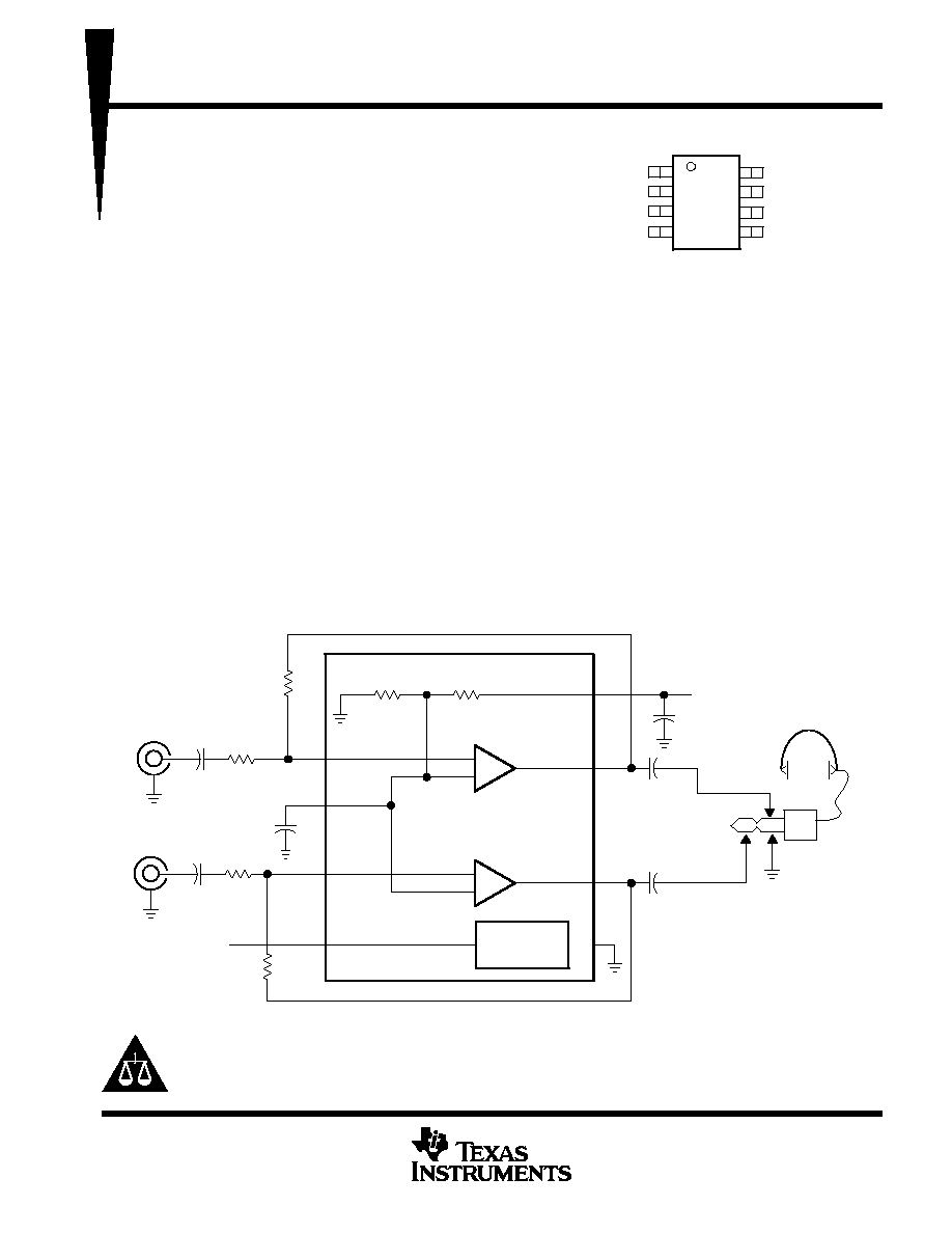
typical application circuit
Audio
Input
Bias
Control
8
1
7
4
VO1
VO2
VDD
5
2
3
6
IN 1≠
BYPASS
SHUTDOWN
VDD/2
CI
RI
RF
320 k
320 k
CB
CS
Audio
Input
CI
RI
IN 2≠
RF
VDD
From Shutdown
Control Circuit
≠
+
≠
+
CC
CC
Copyright
©
2000, Texas Instruments Incorporated
PRODUCTION DATA information is current as of publication date.
Products conform to specifications per the terms of Texas Instruments
standard warranty. Production processing does not necessarily include
testing of all parameters.
1
2
3
4
8
7
6
5
V
O
1
IN ≠
BYPASS
GND
V
DD
V
O
2
IN2 ≠
SHUTDOWN
D OR DGN PACKAGE
(TOP VIEW)
PowerPAD is a trademark of Texas Instruments.

TPA122
150-mW STEREO AUDIO POWER AMPLIFIER
SLOS211C ≠ AUGUST1998 ≠ REVISED MARCH 2000
2
POST OFFICE BOX 655303
∑
DALLAS, TEXAS 75265
AVAILABLE OPTIONS
PACKAGED DEVICES
MSOP
TA
SMALL OUTLINE
(D)
MSOP
(DGN)
MSOP
Symbolization
≠ 40
∞
C to 85
∞
C
TPA122D
TPA122DGN
TI AAE
The D and DGN package is available in left-ended tape and reel only (e.g., TPA122DR,
TPA122DGNR).
Terminal Functions
TERMINAL
I/O
DESCRIPTION
NAME
NO.
I/O
DESCRIPTION
BYPASS
3
I
Tap to voltage divider for internal mid-supply bias supply. Connect to a 0.1
µ
F to 1
µ
F low ESR capacitor for
best performance.
GND
4
I
GND is the ground connection.
IN1≠
2
I
IN1≠ is the inverting input for channel 1.
IN2≠
6
I
IN2≠ is the inverting input for channel 2.
SHUTDOWN
5
I
Puts the device in a low quiescent current mode when held high
VDD
8
I
VDD is the supply voltage terminal.
VO1
1
O
VO1 is the audio output for channel 1.
VO2
7
O
VO2 is the audio output for channel 2.
absolute maximum ratings over operating free-air temperature (unless otherwise noted)
Supply voltage, V
DD
6 V
. . . . . . . . . . . . . . . . . . . . . . . . . . . . . . . . . . . . . . . . . . . . . . . . . . . . . . . . . . . . . . . . . . . . . . . .
Input voltage, V
I
≠0.3 V to V
DD
+ 0.3 V
. . . . . . . . . . . . . . . . . . . . . . . . . . . . . . . . . . . . . . . . . . . . . . . . . . . . . . . . . . . .
Continuous total power dissipation
internally limited
. . . . . . . . . . . . . . . . . . . . . . . . . . . . . . . . . . . . . . . . . . . . . . . . .
Operating junction temperature range, T
J
≠40
∞
C to 150
∞
C
. . . . . . . . . . . . . . . . . . . . . . . . . . . . . . . . . . . . . . . . . . .
Storage temperature range, T
stg
≠ 65
∞
C to 150
∞
C
. . . . . . . . . . . . . . . . . . . . . . . . . . . . . . . . . . . . . . . . . . . . . . . . . . .
Lead temperature 1,6 mm (1/16 inch) from case for 10 seconds
260
∞
C
. . . . . . . . . . . . . . . . . . . . . . . . . . . . . . .
Stresses beyond those listed under "absolute maximum ratings" may cause permanent damage to the device. These are stress ratings only, and
functional operation of the device at these or any other conditions beyond those indicated under "recommended operating conditions" is not
implied. Exposure to absolute-maximum-rated conditions for extended periods may affect device reliability.
DISSIPATION RATING TABLE
PACKAGE
TA
25
∞
C
POWER RATING
DERATING FACTOR
ABOVE TA = 25
∞
C
TA = 70
∞
C
POWER RATING
TA = 85
∞
C
POWER RATING
D
725 mW
5.8 mW/
∞
C
464 mW
377 mW
DGN
2.14 W
17.1 mW/
∞
C
1.37 W
1.11 W
Please see the Texas Instruments document, PowerPAD Thermally Enhanced Package Application Report
(literature number SLMA002), for more information on the PowerPAD package. The thermal data was
measured on a PCB layout based on the information in the section entitled
Texas Instruments Recommended
Board for PowerPAD on page 33 of the before mentioned document.
recommended operating conditions
MIN
MAX
UNIT
Supply voltage, VDD
2.5
5.5
V
Operating free-air temperature, TA
≠40
85
∞
C

TPA122
150-mW STEREO AUDIO POWER AMPLIFIER
SLOS211C ≠ AUGUST1998 ≠ REVISED MARCH 2000
3
POST OFFICE BOX 655303
∑
DALLAS, TEXAS 75265
dc electrical characteristics at T
A
= 25
∞
C, V
DD
= 3.3 V
PARAMETER
TEST CONDITIONS
MIN
TYP
MAX
UNIT
VIO
Input offset voltage
5
mV
PSRR
Power supply rejection ratio
VDD = 3.2 V to 3.4 V
83
dB
IDD
Supply current
1.5
3
mA
IDD(SD)
Supply current in SHUTDOWN mode
10
50
µ
A
ZI
Input impedance
> 1
M
ac operating characteristics, V
DD
= 3.3 V, T
A
= 25
∞
C, R
L
= 8
PARAMETER
TEST CONDITIONS
MIN
TYP
MAX
UNIT
PO
Output power (each channel)
THD
0.1%
70
mW
THD+N
Total harmonic distortion + noise
PO = 70 mW,
20≠20 kHz
2%
BOM
Maximum output power BW
G = 10,
THD <5%
>20
kHz
Phase margin
Open loop
58
∞
Supply ripple rejection
f = 1 kHz
68
dB
Channel/Channel output separation
f = 1 kHz
86
dB
SNR
Signal-to-noise ratio
PO = 100 mW
100
dB
Vn
Noise output voltage
9.5
µ
V(rms)
Measured at 1 kHz
dc electrical characteristics at T
A
= 25
∞
C, V
DD
= 5 V
PARAMETER
TEST CONDITIONS
MIN
TYP
MAX
UNIT
VIO
Input offset voltage
5
mV
PSRR
Power supply rejection ratio
VDD = 4.9 V to 5.1 V
76
dB
IDD
Supply current
1.5
3
mA
IDD(SD)
Supply current in SHUTDOWN mode
60
100
µ
A
ZI
Input impedance
> 1
M
ac operating characteristics, V
DD
= 5 V, T
A
= 25
∞
C, R
L
= 8
PARAMETER
TEST CONDITIONS
MIN
TYP
MAX
UNIT
PO
Output power (each channel)
THD
0.1%
70
mW
THD+N
Total harmonic distortion + noise
PO = 150 mW, 20≠20 kHz
2%
BOM
Maximum output power BW
G = 10,
THD <5%
>20
kHz
Phase margin
Open loop
56
∞
Supply ripple rejection ratio
f = 1 kHz
68
dB
Channel/channel output separation
f = 1 kHz
86
dB
SNR
Signal-to-noise ratio
PO = 150 mW
100
dB
Vn
Noise output voltage
9.5
µ
V(rms)
Measured at 1 kHz

TPA122
150-mW STEREO AUDIO POWER AMPLIFIER
SLOS211C ≠ AUGUST1998 ≠ REVISED MARCH 2000
4
POST OFFICE BOX 655303
∑
DALLAS, TEXAS 75265
ac operating characteristics, V
DD
= 3.3 V, T
A
= 25
∞
C, R
L
= 32
PARAMETER
TEST CONDITIONS
MIN
TYP
MAX
UNIT
PO
Output power (each channel)
THD
0.1%
40
mW
THD+N
Total harmonic distortion + noise
PO = 30 mW,
20≠20 kHz
0.5%
BOM
Maximum output power BW
G = 10,
THD <2%
>20
kHz
Phase margin
Open loop
58
∞
Supply ripple rejection
f = 1 kHz
68
dB
Channel/channel output separation
f = 1 kHz
86
dB
SNR
Signal-to-noise ratio
PO = 100 mW
100
dB
Vn
Noise output voltage
9.5
µ
V(rms)
Measured at 1 kHz
ac operating characteristics, V
DD
= 5 V, T
A
= 25
∞
C, R
L
= 32
PARAMETER
TEST CONDITIONS
MIN
TYP
MAX
UNIT
PO
Output power (each channel)
THD
0.1%
40
mW
THD+N
Total harmonic distortion + noise
PO = 60 mW,
20≠20 kHz
0.4%
BOM
Maximum output power BW
G = 10,
THD <2%
>20
kHz
Phase margin
Open loop
56
∞
Supply ripple rejection
f = 1 kHz
68
dB
Channel/channel output separation
f = 1 kHz
86
dB
SNR
Signal-to-noise ratio
PO = 150 mW
100
dB
Vn
Noise output voltage
9.5
µ
V(rms)
Measured at 1 kHz

TPA122
150-mW STEREO AUDIO POWER AMPLIFIER
SLOS211C ≠ AUGUST1998 ≠ REVISED MARCH 2000
5
POST OFFICE BOX 655303
∑
DALLAS, TEXAS 75265
TYPICAL CHARACTERISTICS
Table of Graphs
FIGURE
THD+N
Total harmonic distortion plus noise
vs Frequency
1, 2, 4, 5, 7, 8,
10, 11, 13, 14,
16, 17, 34, 36
vs Power output
3, 6, 9,
12, 15, 18
Supply ripple rejection
vs Frequency
19, 20
Vn
Output noise voltage
vs Frequency
21, 22
Crosstalk
vs Frequency
23 ≠ 26,
37, 38
Mute attenuation
vs Frequency
27, 28
Open-loop gain and phase margin
vs Frequency
29, 30
Output power
vs Load resistance
31, 32
Closed-Loop gain and phase
vs Frequency
39 ≠ 44
Output power
vs Load resistance
31, 32
IDD
Supply current
vs Supply voltage
33
SNR
Signal-to-noise ratio
vs Voltage gain
35
Closed-loop gain
vs Frequency
39 ≠ 44
Power dissipation/amplifier
vs Output power
45, 46